Chapter 8 Synchronous Sequential Circuits W Combinational circuit
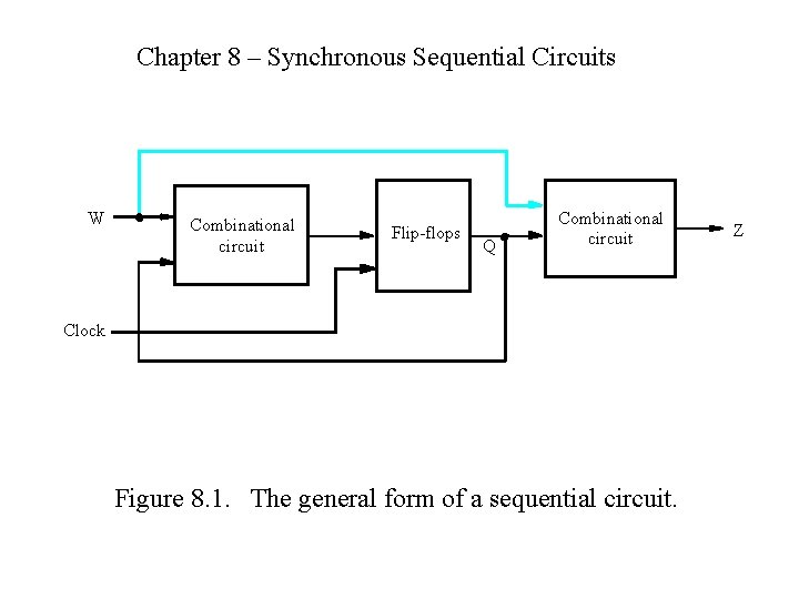
Chapter 8 – Synchronous Sequential Circuits W Combinational circuit Flip-flops Q Combinational circuit Clock Figure 8. 1. The general form of a sequential circuit. Z
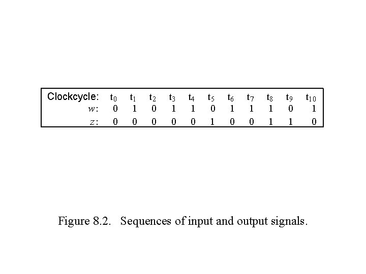
Clockcycle: w: z: t 0 0 0 t 1 1 0 t 2 0 0 t 3 1 0 t 4 1 0 t 5 0 1 t 6 1 0 t 7 1 0 t 8 1 1 t 9 0 1 t 10 1 0 Figure 8. 2. Sequences of input and output signals.
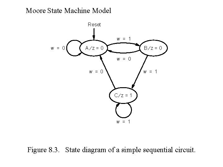
Moore State Machine Model Reset w = 1 w = 0 A¤z=0 B¤z= 0 w = 1 w = 0 C¤z = 1 w = 1 Figure 8. 3. State diagram of a simple sequential circuit.
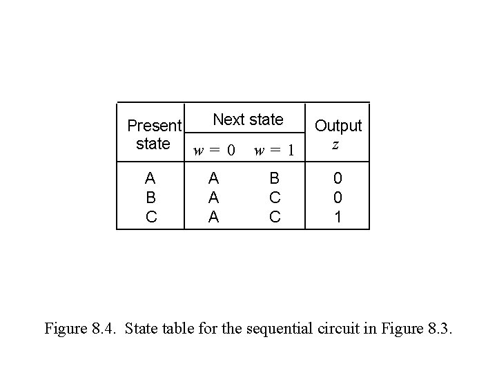
Next state Present state w = 0 w = 1 A B C A A A B C C Output z 0 0 1 Figure 8. 4. State table for the sequential circuit in Figure 8. 3.
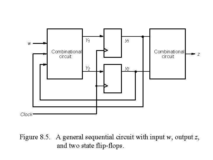
Y 1 w y 1 Combinational circuit Y 2 z y 2 Clock Figure 8. 5. A general sequential circuit with input w, output z, and two state flip-flops.
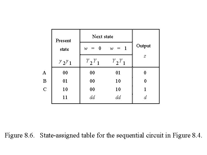
Present state Next state w = 0 w = 1 Output z y y 2 1 Y Y 2 1 A 00 00 01 0 B 01 00 10 0 C 10 00 10 1 11 dd dd d Figure 8. 6. State-assigned table for the sequential circuit in Figure 8. 4.
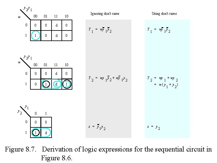
y y 2 1 w 0 00 01 11 10 0 0 d 0 Ignoring don't cares Y 1 w 1 0 d 0 00 01 11 10 0 0 d 0 1 = wy y 1 2 Y 2 = wy y + wy y 1 2 Y 1 = wy y 1 2 y y 2 1 0 Y 1 y y Using don't cares 0 1 0 0 d 1 2 = wy + wy 1 2 = w(y + y ) 1 2 0 1 1 d z = y y 1 2 z = y 2 Figure 8. 7. Derivation of logic expressions for the sequential circuit in Figure 8. 6.
Figure 8. 8. Final implementation of the sequential circuit derived in Figure 8. 7.
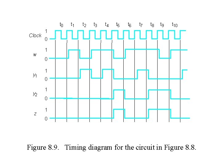
t 0 Clock w y 1 y 2 z t 1 t 2 t 3 t 4 t 5 t 6 t 7 t 8 t 9 t 10 1 0 1 0 1 0 Figure 8. 9. Timing diagram for the circuit in Figure 8. 8.
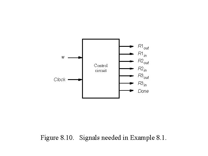
R 1 out R 1 in w Control circuit Clock R 2 out R 2 in R 3 out R 3 in Done Figure 8. 10. Signals needed in Example 8. 1.
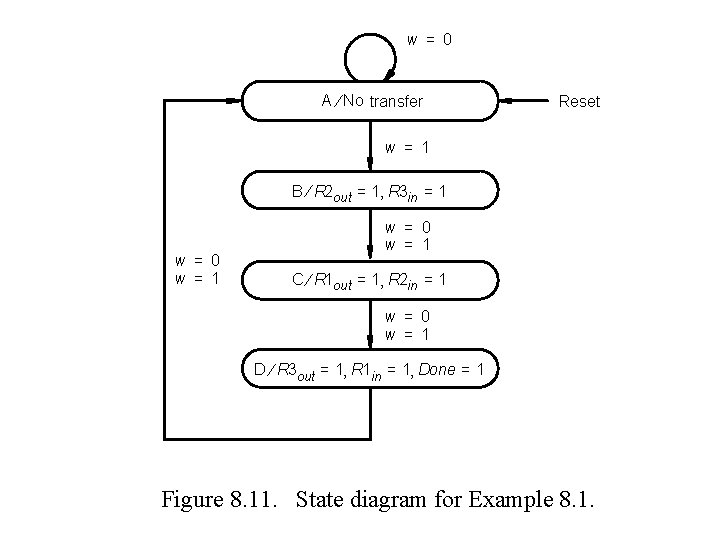
w = 0 A ¤ No transfer Reset w = 1 B ¤ R 2 out = 1, R 3 in = 1 w = 0 w = 1 C ¤ R 1 out = 1, R 2 in = 1 w = 0 w = 1 D ¤ R 3 out = 1, R 1 in = 1, Done = 1 Figure 8. 11. State diagram for Example 8. 1.
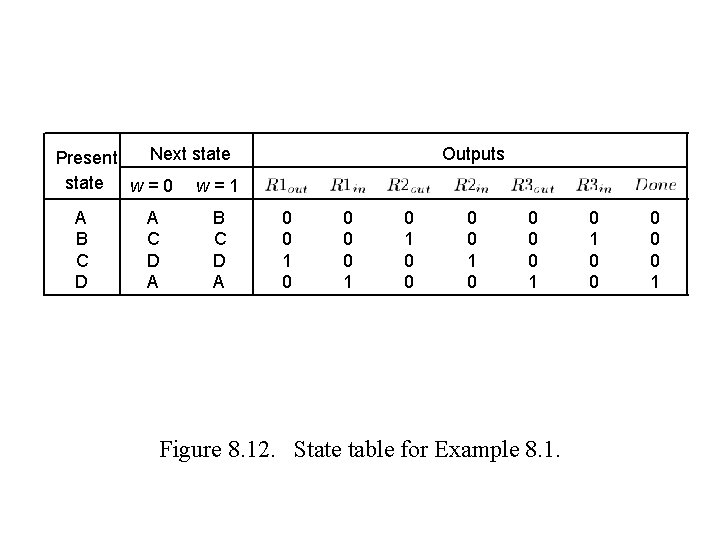
Next state Present state w = 0 w = 1 A B C D A Outputs 0 0 1 0 0 1 Figure 8. 12. State table for Example 8. 1. 0 1 0 0 0 1
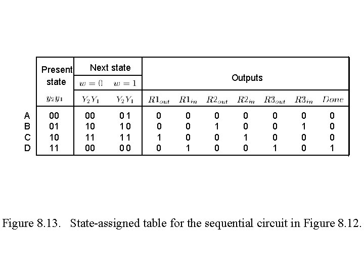
Present state A B C D 00 01 10 11 Next state Outputs 00 10 11 00 01 10 11 00 0 0 1 0 1 0 0 0 1 Figure 8. 13. State-assigned table for the sequential circuit in Figure 8. 12.
Figure 8. 14. Derivation of next-state expressions for the sequential circuit in Figure 8. 13.
Figure 8. 15. Final implementation of sequential circuit in Figure 8. 13.
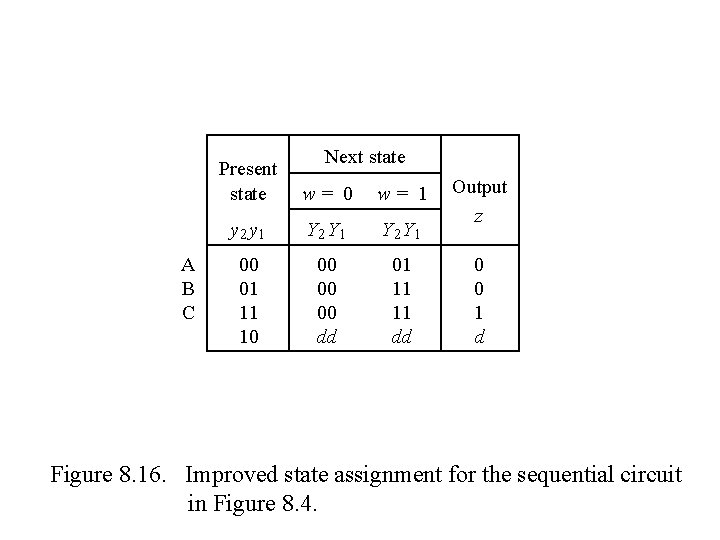
A B C Next state Present state w= 0 w= 1 y 2 y 1 Y 2 Y 1 00 01 11 10 00 00 00 dd 01 11 11 dd Output z 0 0 1 d Figure 8. 16. Improved state assignment for the sequential circuit in Figure 8. 4.
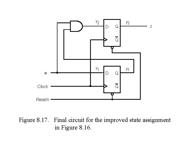
Y 2 D Q y 2 z Q w Clock Y 1 D Q y 1 Q Resetn Figure 8. 17. Final circuit for the improved state assignment in Figure 8. 16.
Figure 8. 18. Improved state assignment for the sequential circuit in Figure 8. 12.
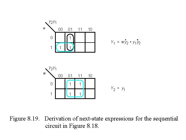
y 2 y 1 w 00 0 1 w 01 11 10 1 Y 1 = wy 2 + y 1 y 2 1 1 00 01 11 0 1 1 1 y 2 y 1 10 Y 2 = y 1 Figure 8. 19. Derivation of next-state expressions for the sequential circuit in Figure 8. 18.
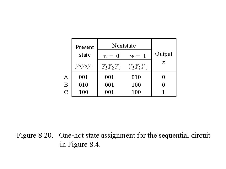
A B C Nextstate Present state w= 0 w= 1 y 3 y 2 y 1 Y 3 Y 2 Y 1 001 010 100 001 001 010 100 Output z 0 0 1 Figure 8. 20. One-hot state assignment for the sequential circuit in Figure 8. 4.
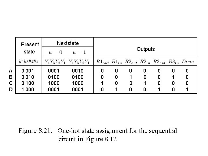
Present state A B C D 0 001 0 010 0 100 1 000 Nextstate Outputs 0001 0100 1000 0001 0010 0100 1000 0001 0 0 0 0 1 0 1 0 0 Figure 8. 21. One-hot state assignment for the sequential circuit in Figure 8. 12. 0 0 0 1
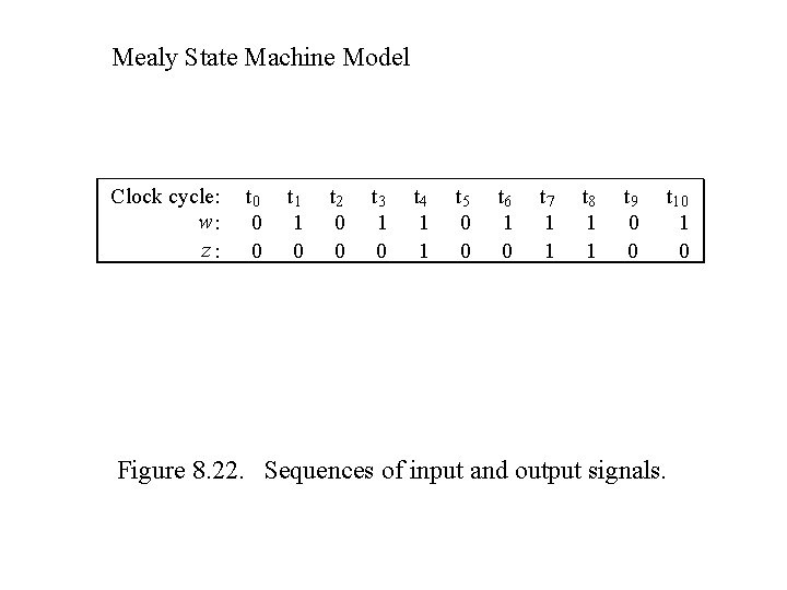
Mealy State Machine Model Clock cycle: w: z: t 0 0 0 t 1 1 0 t 2 0 0 t 3 1 0 t 4 1 1 t 5 0 0 t 6 1 0 t 7 1 1 t 8 1 1 t 9 0 0 t 10 1 0 Figure 8. 22. Sequences of input and output signals.
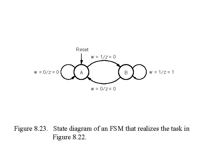
Reset w = 1¤z= 0 w = 0¤z= 0 A B w = 1¤z= 1 w = 0¤z= 0 Figure 8. 23. State diagram of an FSM that realizes the task in Figure 8. 22.
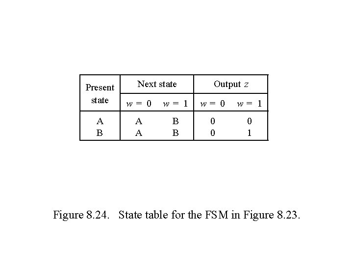
Next state Output z Present state w= 0 w= 1 A B A A B B 0 0 0 1 Figure 8. 24. State table for the FSM in Figure 8. 23.
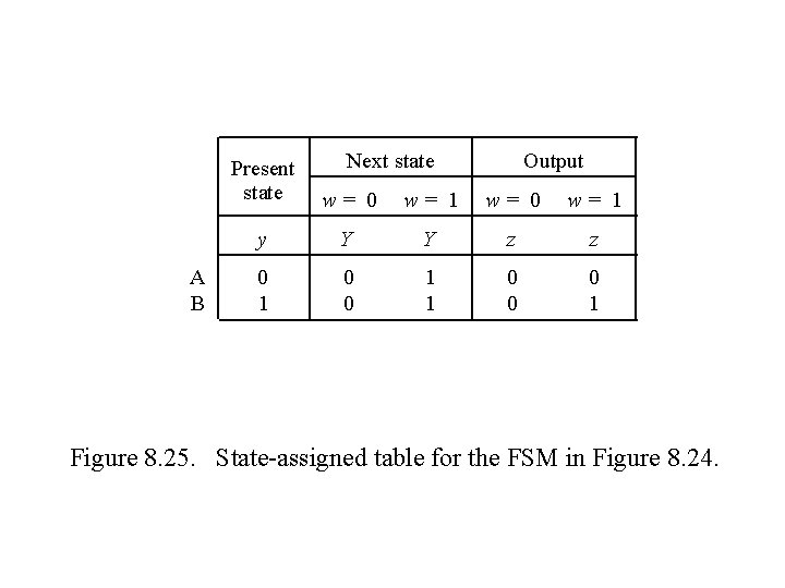
A B Next state Output Present state w= 0 w= 1 y Y Y z z 0 1 0 0 1 1 0 0 0 1 Figure 8. 25. State-assigned table for the FSM in Figure 8. 24.
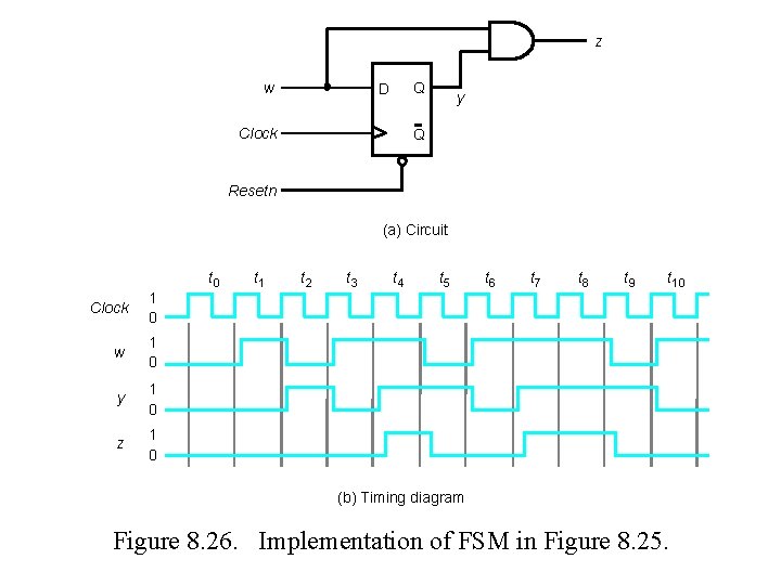
z w Q D Clock y Q Resetn (a) Circuit Clock 1 0 w 1 0 y 1 0 z 1 0 t 1 t 2 t 3 t 4 t 5 t 6 t 7 t 8 t 9 t 10 (b) Timing diagram Figure 8. 26. Implementation of FSM in Figure 8. 25.
Figure 8. 27. Circuit that implements the specification in Figure 8. 2.
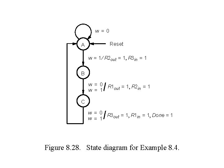
w = 0 A Reset w = 1 ¤ R 2 out = 1, R 3 in = 1 B w = 0 R 1 = 1, R 2 = 1 out in w = 1 C w = 0 R 3 = 1, R 1 = 1, Done = 1 out in w = 1 Figure 8. 28. State diagram for Example 8. 4.
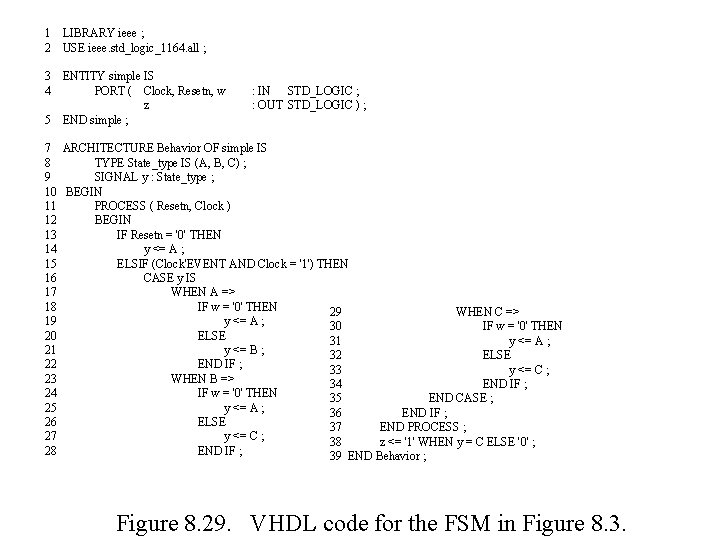
1 2 LIBRARY ieee ; USE ieee. std_logic_1164. all ; 3 4 ENTITY simple IS PORT ( Clock, Resetn, w z END simple ; 5 : IN STD_LOGIC ; : OUT STD_LOGIC ) ; 7 ARCHITECTURE Behavior OF simple IS 8 TYPE State_type IS (A, B, C) ; 9 SIGNAL y : State_type ; 10 BEGIN 11 PROCESS ( Resetn, Clock ) 12 BEGIN 13 IF Resetn = '0' THEN 14 y <= A ; 15 ELSIF (Clock'EVENT AND Clock = '1') THEN 16 CASE y IS 17 WHEN A => 18 IF w = '0' THEN 29 WHEN C => 19 y <= A ; 30 IF w = '0' THEN 20 ELSE 31 y <= A ; 21 y <= B ; 32 ELSE 22 END IF ; 33 y <= C ; 23 WHEN B => 34 END IF ; 24 IF w = '0' THEN 35 END CASE ; 25 y <= A ; 36 END IF ; 26 ELSE 37 END PROCESS ; 27 y <= C ; 38 z <= '1' WHEN y = C ELSE '0' ; 28 END IF ; 39 END Behavior ; Figure 8. 29. VHDL code for the FSM in Figure 8. 3.
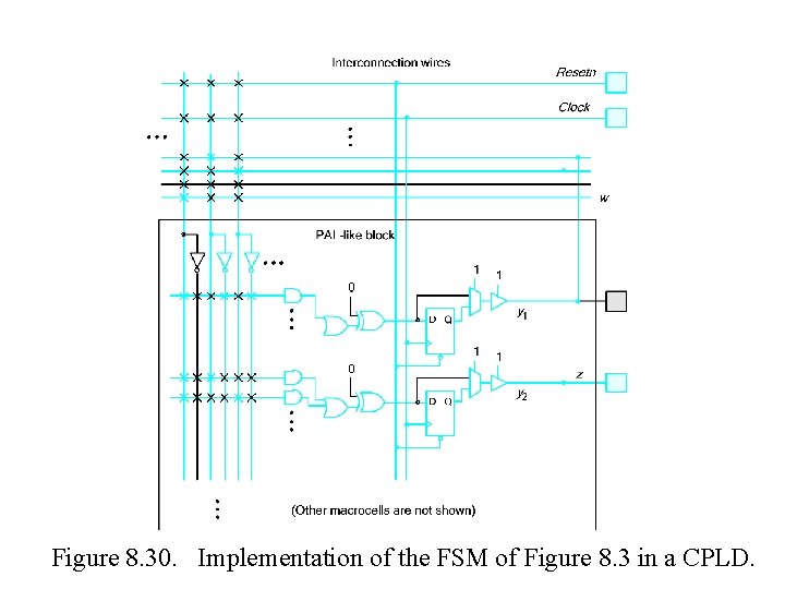
Figure 8. 30. Implementation of the FSM of Figure 8. 3 in a CPLD.
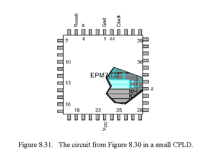
Figure 8. 31. The circuit from Figure 8. 30 in a small CPLD.
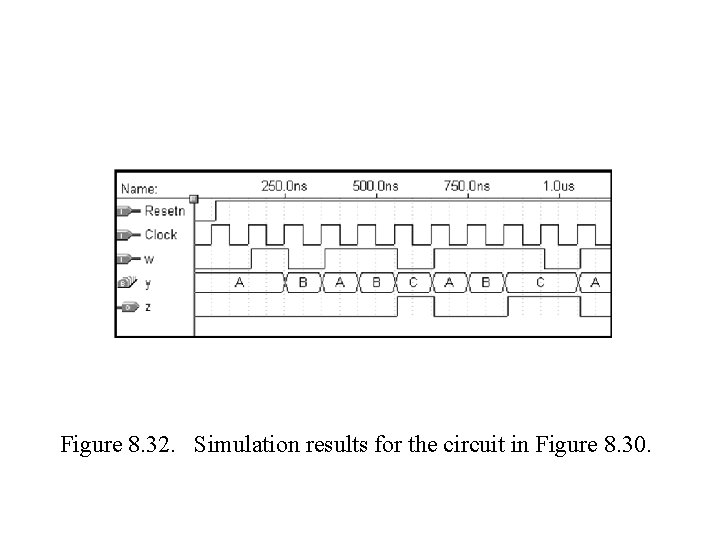
Figure 8. 32. Simulation results for the circuit in Figure 8. 30.

ARCHITECTURE Behavior OF simple IS TYPE State_type IS (A, B, C) ; SIGNAL y_present, y_next : State_type ; BEGIN PROCESS ( w, y_present ) BEGIN CASE y_present IS WHEN A => IF w = '0' THEN y_next <= A ; ELSE y_next <= B ; END IF ; WHEN B => IF w = '0' THEN y_next <= A ; ELSE y_next <= C ; END IF ; WHEN C => IF w = '0' THEN y_next <= A ; ELSE y_next <= C ; END IF ; END CASE ; END PROCESS ; PROCESS (Clock, Resetn) BEGIN IF Resetn = '0' THEN y_present <= A ; ELSIF (Clock'EVENT AND Clock = '1') THEN y_present <= y_next ; END IF ; END PROCESS ; z <= '1' WHEN y_present = C ELSE '0' ; END Behavior ; Figure 8. 33. Alternative style of VHDL code for the FSM in Figure 8. 3.
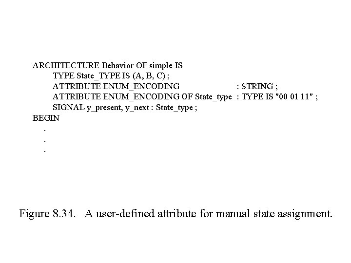
ARCHITECTURE Behavior OF simple IS TYPE State_TYPE IS (A, B, C) ; ATTRIBUTE ENUM_ENCODING : STRING ; ATTRIBUTE ENUM_ENCODING OF State_type : TYPE IS "00 01 11" ; SIGNAL y_present, y_next : State_type ; BEGIN. . . Figure 8. 34. A user-defined attribute for manual state assignment.
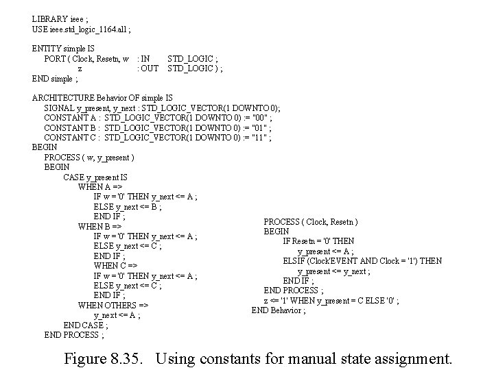
LIBRARY ieee ; USE ieee. std_logic_1164. all ; ENTITY simple IS PORT ( Clock, Resetn, w z END simple ; : IN : OUT STD_LOGIC ; STD_LOGIC ) ; ARCHITECTURE Behavior OF simple IS SIGNAL y_present, y_next : STD_LOGIC_VECTOR(1 DOWNTO 0); CONSTANT A : STD_LOGIC_VECTOR(1 DOWNTO 0) : = "00" ; CONSTANT B : STD_LOGIC_VECTOR(1 DOWNTO 0) : = "01" ; CONSTANT C : STD_LOGIC_VECTOR(1 DOWNTO 0) : = "11" ; BEGIN PROCESS ( w, y_present ) BEGIN CASE y_present IS WHEN A => IF w = '0' THEN y_next <= A ; ELSE y_next <= B ; END IF ; PROCESS ( Clock, Resetn ) WHEN B => BEGIN IF w = '0' THEN y_next <= A ; IF Resetn = '0' THEN ELSE y_next <= C ; y_present <= A ; END IF ; ELSIF (Clock'EVENT AND Clock = '1') THEN WHEN C => y_present <= y_next ; IF w = '0' THEN y_next <= A ; END IF ; ELSE y_next <= C ; END PROCESS ; END IF ; z <= '1' WHEN y_present = C ELSE '0' ; WHEN OTHERS => END Behavior ; y_next <= A ; END CASE ; END PROCESS ; Figure 8. 35. Using constants for manual state assignment.
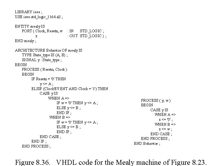
LIBRARY ieee ; USE ieee. std_logic_1164. all ; ENTITY mealy IS PORT ( Clock, Resetn, w z END mealy ; : IN STD_LOGIC ; : OUT STD_LOGIC ) ; ARCHITECTURE Behavior OF mealy IS TYPE State_type IS (A, B) ; SIGNAL y : State_type ; BEGIN PROCESS ( Resetn, Clock ) BEGIN IF Resetn = '0' THEN y <= A ; ELSIF (Clock'EVENT AND Clock = '1') THEN CASE y IS WHEN A => IF w = '0' THEN y <= A ; ELSE y <= B ; END IF ; WHEN B => IF w = '0' THEN y <= A ; ELSE y <= B ; END IF ; END CASE ; END IF ; END PROCESS ; PROCESS ( y, w ) BEGIN CASE y IS WHEN A => z <= '0' ; WHEN B => z <= w ; END CASE ; END PROCESS ; END Behavior ; Figure 8. 36. VHDL code for the Mealy machine of Figure 8. 23.
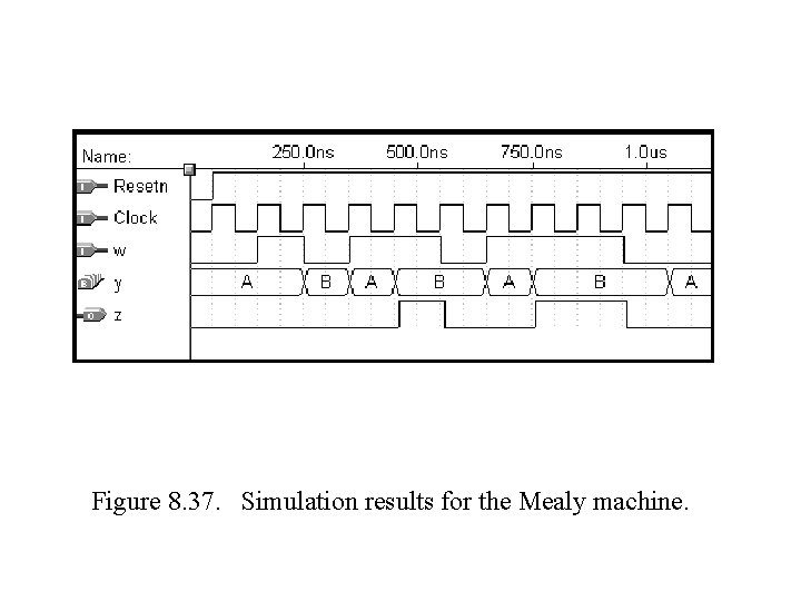
Figure 8. 37. Simulation results for the Mealy machine.
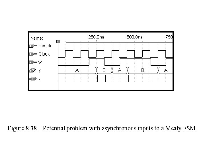
Figure 8. 38. Potential problem with asynchronous inputs to a Mealy FSM.
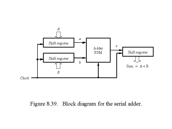
A a Shift register Adder FSM Shift register b s Shift register Sum = A + B B Clock Figure 8. 39. Block diagram for the serial adder.
Figure 8. 40. State diagram for the serial adder FSM.
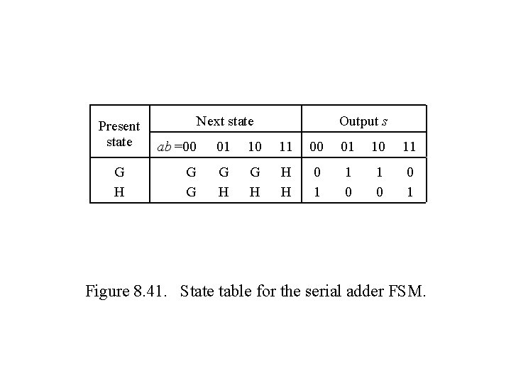
Present state G H Output s Next state ab =00 01 10 11 G G G H H H 0 1 1 0 0 1 Figure 8. 41. State table for the serial adder FSM.
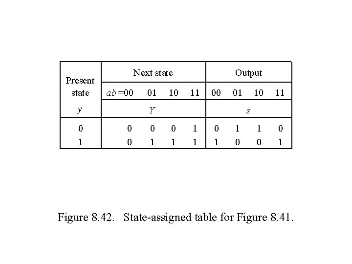
Present state Next state ab =00 y 0 1 01 10 Output 11 00 01 Y 0 0 0 1 10 11 1 0 0 1 s 0 1 1 1 0 Figure 8. 42. State-assigned table for Figure 8. 41.
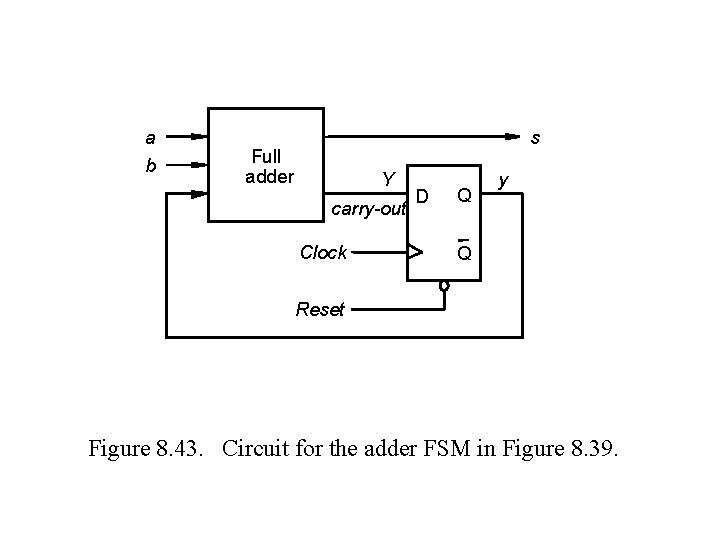
a b s Full adder Y carry-out Clock D Q y Q Reset Figure 8. 43. Circuit for the adder FSM in Figure 8. 39.
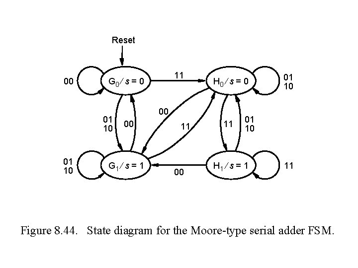
Reset 00 01 10 11 G 0 ¤ s = 0 H 0 ¤ s = 0 00 00 G 1 ¤ s = 1 11 00 11 01 10 H 1 ¤ s = 1 11 Figure 8. 44. State diagram for the Moore-type serial adder FSM.
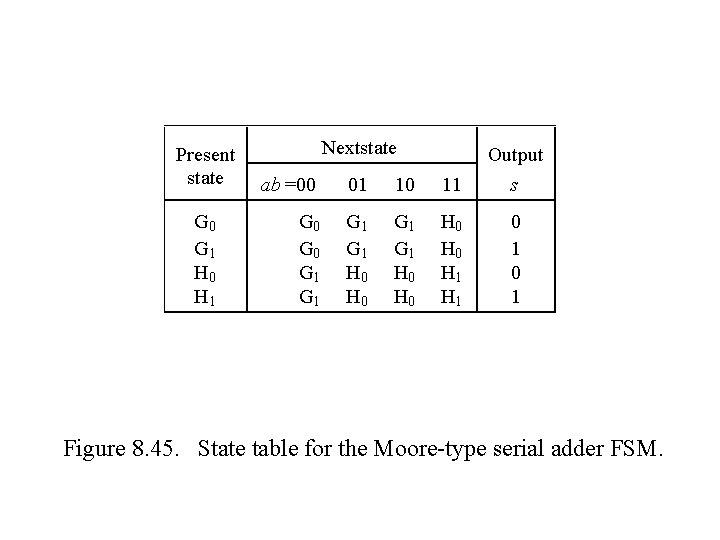
Present state G 0 G 1 H 0 H 1 Nextstate ab =00 01 10 11 Output s G 0 G 1 G 1 H 0 H 0 H 1 0 1 Figure 8. 45. State table for the Moore-type serial adder FSM.
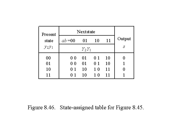
Present state y 2 y 1 00 01 10 11 Nextstate ab =00 01 10 11 s Y 2 Y 1 00 00 01 01 10 10 Output 01 01 10 10 11 11 0 1 Figure 8. 46. State-assigned table for Figure 8. 45.
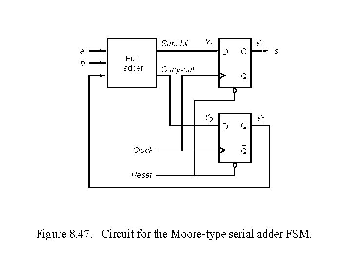
a b Sum bit Full adder Y 1 Carry-out Q s Q Y 2 Clock D y 1 D Q y 2 Q Reset Figure 8. 47. Circuit for the Moore-type serial adder FSM.
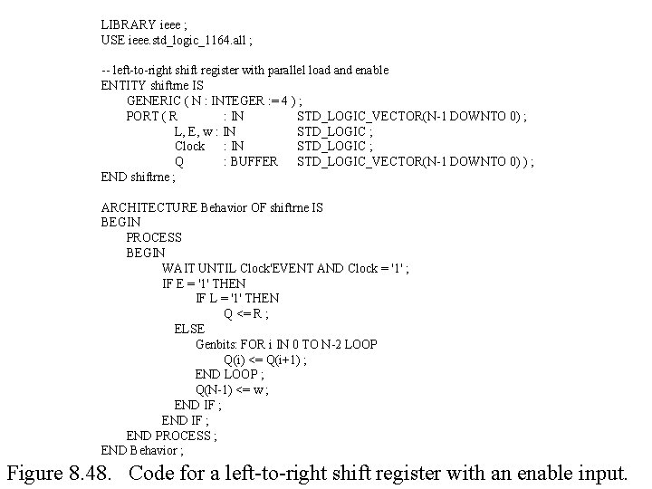
LIBRARY ieee ; USE ieee. std_logic_1164. all ; -- left-to-right shift register with parallel load and enable ENTITY shiftrne IS GENERIC ( N : INTEGER : = 4 ) ; PORT ( R : IN STD_LOGIC_VECTOR(N-1 DOWNTO 0) ; L, E, w : IN STD_LOGIC ; Clock : IN STD_LOGIC ; Q : BUFFER STD_LOGIC_VECTOR(N-1 DOWNTO 0) ) ; END shiftrne ; ARCHITECTURE Behavior OF shiftrne IS BEGIN PROCESS BEGIN WAIT UNTIL Clock'EVENT AND Clock = '1' ; IF E = '1' THEN IF L = '1' THEN Q <= R ; ELSE Genbits: FOR i IN 0 TO N-2 LOOP Q(i) <= Q(i+1) ; END LOOP ; Q(N-1) <= w ; END IF ; END PROCESS ; END Behavior ; Figure 8. 48. Code for a left-to-right shift register with an enable input.
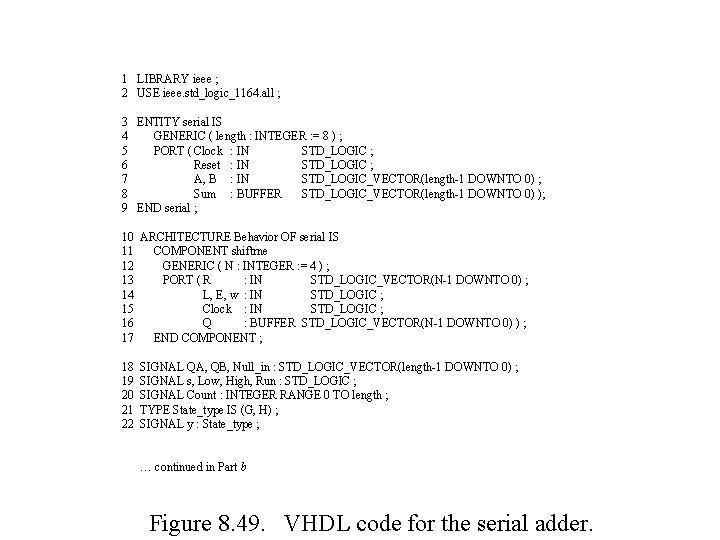
1 LIBRARY ieee ; 2 USE ieee. std_logic_1164. all ; 3 ENTITY serial IS 4 GENERIC ( length : INTEGER : = 8 ) ; 5 PORT ( Clock : IN STD_LOGIC ; 6 Reset : IN STD_LOGIC ; 7 A, B : IN STD_LOGIC_VECTOR(length-1 DOWNTO 0) ; 8 Sum : BUFFER STD_LOGIC_VECTOR(length-1 DOWNTO 0) ); 9 END serial ; 10 ARCHITECTURE Behavior OF serial IS 11 COMPONENT shiftrne 12 GENERIC ( N : INTEGER : = 4 ) ; 13 PORT ( R : IN STD_LOGIC_VECTOR(N-1 DOWNTO 0) ; 14 L, E, w : IN STD_LOGIC ; 15 Clock : IN STD_LOGIC ; 16 Q : BUFFER STD_LOGIC_VECTOR(N-1 DOWNTO 0) ) ; 17 END COMPONENT ; 18 19 20 21 22 SIGNAL QA, QB, Null_in : STD_LOGIC_VECTOR(length-1 DOWNTO 0) ; SIGNAL s, Low, High, Run : STD_LOGIC ; SIGNAL Count : INTEGER RANGE 0 TO length ; TYPE State_type IS (G, H) ; SIGNAL y : State_type ; … continued in Part b Figure 8. 49. VHDL code for the serial adder.
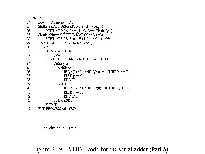
23 BEGIN 24 Low <= '0' ; High <= '1' ; 25 Shift. A: shiftrne GENERIC MAP (N => length) 26 PORT MAP ( A, Reset, High, Low, Clock, QA ) ; 27 Shift. B: shiftrne GENERIC MAP (N => length) 28 PORT MAP ( B, Reset, High, Low, Clock, QB ) ; 29 Adder. FSM: PROCESS ( Reset, Clock ) 30 BEGIN 31 IF Reset = '1' THEN 32 y <= G ; 33 ELSIF Clock'EVENT AND Clock = '1' THEN 34 CASE y IS 35 WHEN G => 36 IF QA(0) = '1' AND QB(0) = '1' THEN y <= H ; 37 ELSE y <= G ; 38 END IF ; 39 WHEN H => 40 IF QA(0) = '0' AND QB(0) = '0' THEN y <= G ; 41 ELSE y <= H ; 42 END IF ; 43 END CASE ; 44 END IF ; 45 END PROCESS Adder. FSM ; … continued in Part c Figure 8. 49. VHDL code for the serial adder (Part b).

46 WITH y SELECT 47 s <= QA(0) XOR QB(0) WHEN G, 48 NOT ( QA(0) XOR QB(0) ) WHEN H ; 49 Null_in <= (OTHERS => '0') ; 50 Shift. Sum: shiftrne GENERIC MAP ( N => length ) 51 PORT MAP ( Null_in, Reset, Run, s, Clock, Sum ) ; 52 Stop: PROCESS 53 BEGIN 54 WAIT UNTIL (Clock'EVENT AND Clock = '1') ; 55 IF Reset = '1' THEN 56 Count <= length ; 57 ELSIF Run = '1' THEN 58 Count <= Count -1 ; 59 END IF ; 60 END PROCESS ; 61 Run <= '0' WHEN Count = 0 ELSE '1' ; -- stops counter and Shift. Sum 62 END Behavior ; Figure 8. 49. VHDL code for the serial adder (Part c).
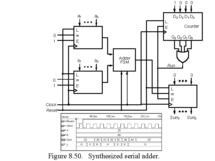
1 0 0 0 a 7 0 1 D 3 D 2 D 1 D 0 L E L w E b 7 0 1 a 0 Counter Q 3 Q 2 Q 1 Q 0 b 0 Adder FSM L w E Run 0 0 L w E Clock Reset Sum 7 Figure 8. 50. Synthesized serial adder. Sum 0
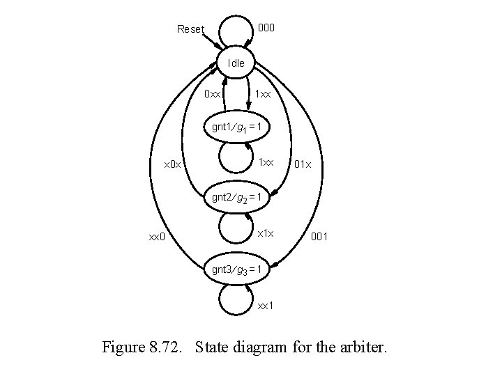
000 Reset Idle 0 xx 1 xx gnt 1 ¤ g 1 = 1 x 0 x 1 xx 01 x gnt 2 ¤ g 2 = 1 xx 0 x 1 x 001 gnt 3 ¤ g 3 = 1 xx 1 Figure 8. 72. State diagram for the arbiter.
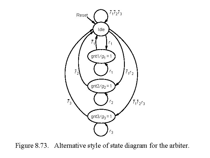
r 1 r 2 r 3 Reset Idle r 1 gnt 1 ¤ g 1 = 1 r 2 r 1 r 2 gnt 2 ¤ g 2 = 1 r 3 r 2 r 1 r 2 r 3 gnt 3 ¤ g 3 = 1 r 3 Figure 8. 73. Alternative style of state diagram for the arbiter.
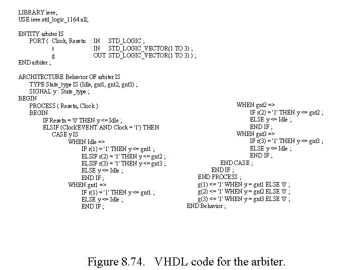
LIBRARY ieee; USE ieee. std_logic_1164. all; ENTITY arbiter IS PORT ( Clock, Resetn : IN STD_LOGIC ; r : IN STD_LOGIC_VECTOR(1 TO 3) ; g : OUT STD_LOGIC_VECTOR(1 TO 3) ) ; END arbiter ; ARCHITECTURE Behavior OF arbiter IS TYPE State_type IS (Idle, gnt 1, gnt 2, gnt 3) ; SIGNAL y : State_type ; BEGIN PROCESS ( Resetn, Clock ) BEGIN IF Resetn = '0' THEN y <= Idle ; ELSIF (Clock'EVENT AND Clock = '1') THEN CASE y IS WHEN Idle => IF r(1) = '1' THEN y <= gnt 1 ; ELSIF r(2) = '1' THEN y <= gnt 2 ; ELSIF r(3) = '1' THEN y <= gnt 3 ; ELSE y <= Idle ; END IF ; WHEN gnt 1 => IF r(1) = '1' THEN y <= gnt 1 ; ELSE y <= Idle ; END IF ; WHEN gnt 2 => IF r(2) = '1' THEN y <= gnt 2 ; ELSE y <= Idle ; END IF ; WHEN gnt 3 => IF r(3) = '1' THEN y <= gnt 3 ; ELSE y <= Idle ; END IF ; END CASE ; END IF ; END PROCESS ; g(1) <= '1' WHEN y = gnt 1 ELSE '0' ; g(2) <= '1' WHEN y = gnt 2 ELSE '0' ; g(3) <= '1' WHEN y = gnt 3 ELSE '0' ; END Behavior ; Figure 8. 74. VHDL code for the arbiter.
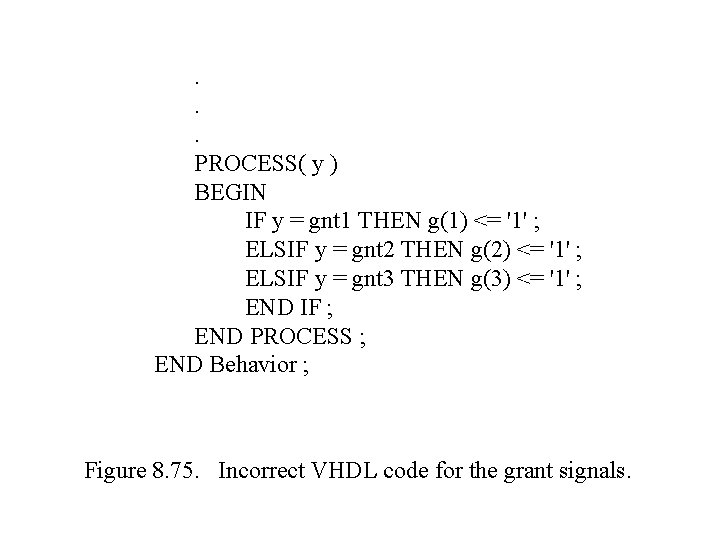
. . . PROCESS( y ) BEGIN IF y = gnt 1 THEN g(1) <= '1' ; ELSIF y = gnt 2 THEN g(2) <= '1' ; ELSIF y = gnt 3 THEN g(3) <= '1' ; END IF ; END PROCESS ; END Behavior ; Figure 8. 75. Incorrect VHDL code for the grant signals.
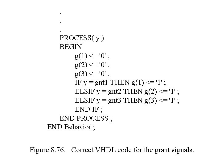
. . . PROCESS( y ) BEGIN g(1) <= '0' ; g(2) <= '0' ; g(3) <= '0' ; IF y = gnt 1 THEN g(1) <= '1' ; ELSIF y = gnt 2 THEN g(2) <= '1' ; ELSIF y = gnt 3 THEN g(3) <= '1' ; END IF ; END PROCESS ; END Behavior ; Figure 8. 76. Correct VHDL code for the grant signals.
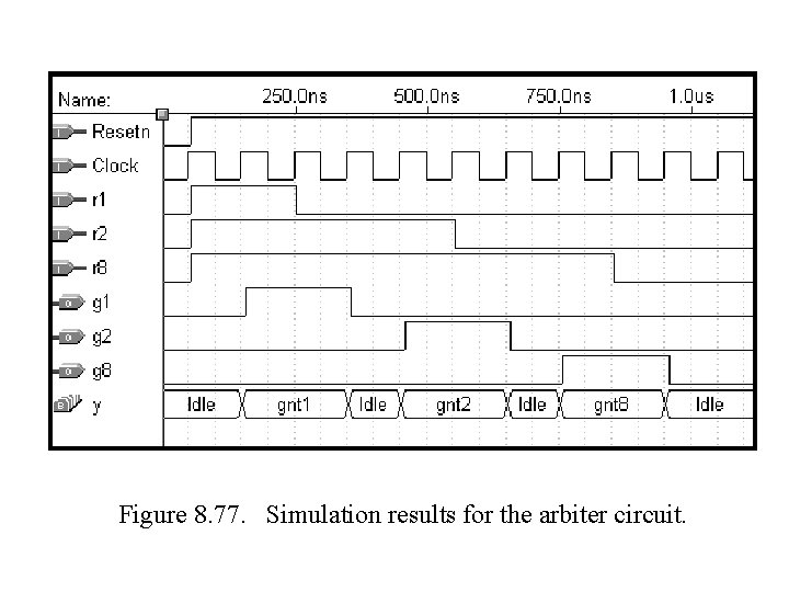
Figure 8. 77. Simulation results for the arbiter circuit.
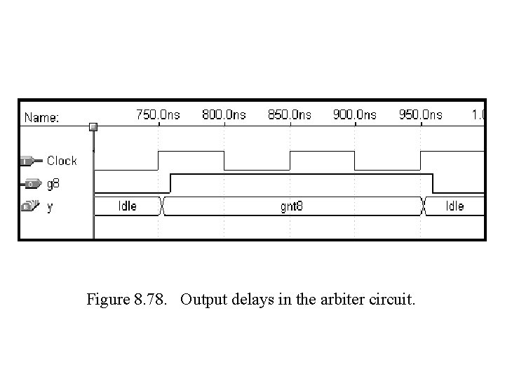
Figure 8. 78. Output delays in the arbiter circuit.
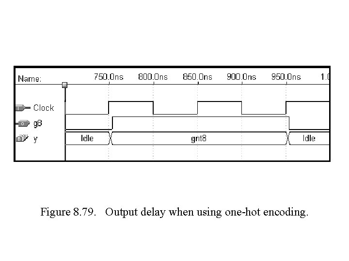
Figure 8. 79. Output delay when using one-hot encoding.
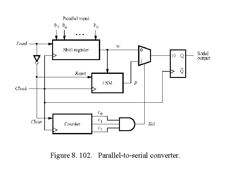
Figure 8. 102. Parallel-to-serial converter.
- Slides: 61