Chapter 8 SPI Protocol and DAC Interfacing STM
![Bits 11: 8 DS [3: 0]: Data size These bits configure the data length Bits 11: 8 DS [3: 0]: Data size These bits configure the data length](https://slidetodoc.com/presentation_image_h2/3c694810fb430b19e93b05260e107cd7/image-15.jpg)
![Bits 15: 0 DR[15: 0]: Data register Data received or to be transmitted. The Bits 15: 0 DR[15: 0]: Data register Data received or to be transmitted. The](https://slidetodoc.com/presentation_image_h2/3c694810fb430b19e93b05260e107cd7/image-19.jpg)
![Bits 2 y: 2 y+1 MODERy[1: 0]: Port x configuration bits (y = 0. Bits 2 y: 2 y+1 MODERy[1: 0]: Port x configuration bits (y = 0.](https://slidetodoc.com/presentation_image_h2/3c694810fb430b19e93b05260e107cd7/image-22.jpg)
- Slides: 32

Chapter 8: SPI Protocol and DAC Interfacing STM 32 F 0 Arm Cortex M 0 Programming for Embedded Systems Using C Language with STM 32 F 0 Nucleo Board by Mazidi, et al. www. microdigitaled. com

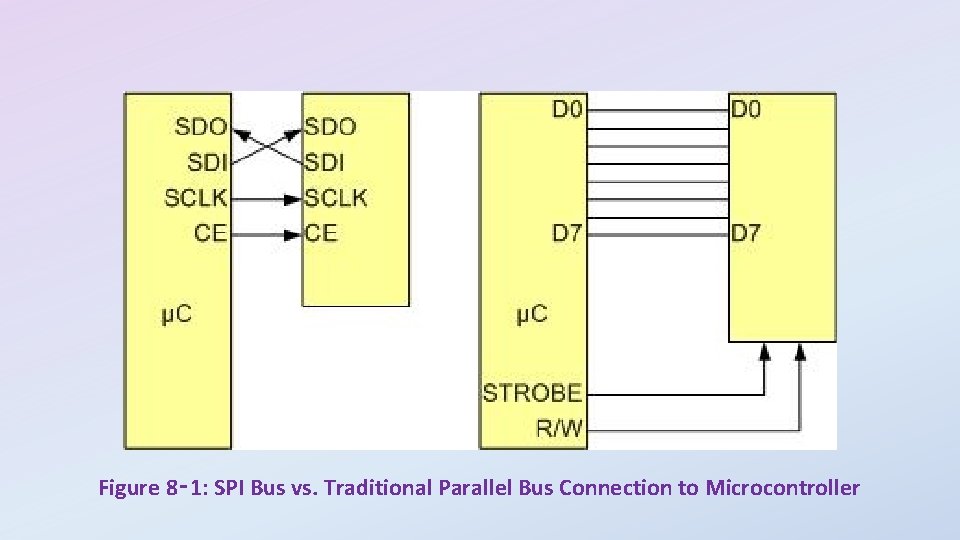
Figure 8‑ 1: SPI Bus vs. Traditional Parallel Bus Connection to Microcontroller

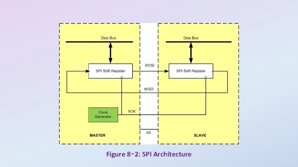
Figure 8‑ 2: SPI Architecture

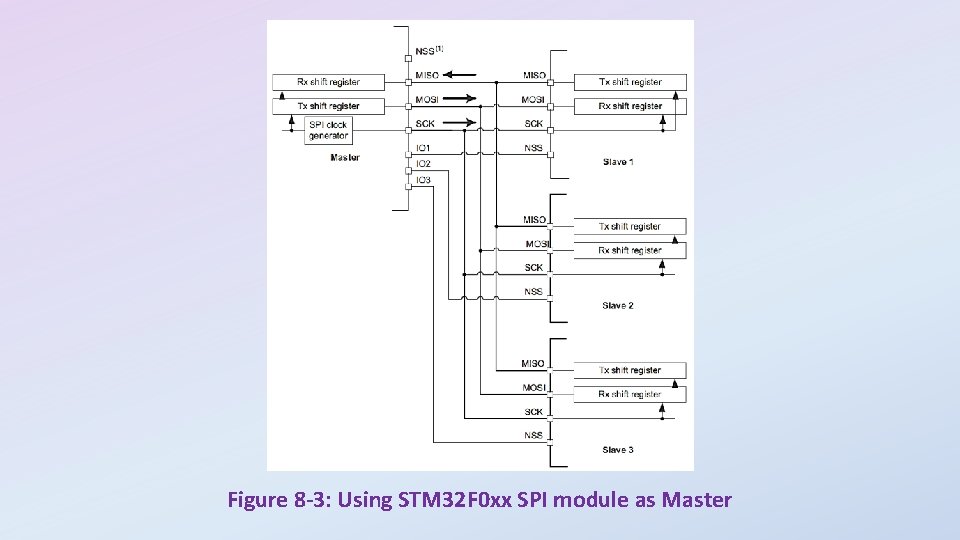
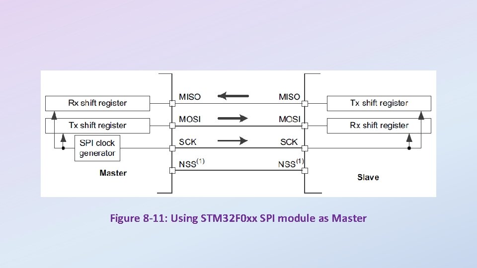
Figure 8 -3: Using STM 32 F 0 xx SPI module as Master

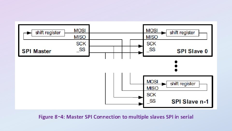
Figure 8‑ 4: Master SPI Connection to multiple slaves SPI in serial

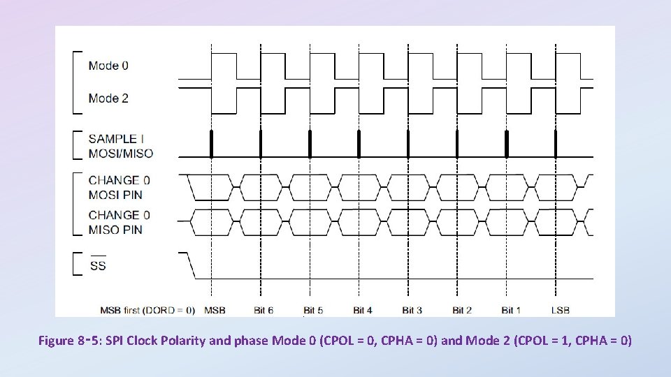
Figure 8‑ 5: SPI Clock Polarity and phase Mode 0 (CPOL = 0, CPHA = 0) and Mode 2 (CPOL = 1, CPHA = 0)

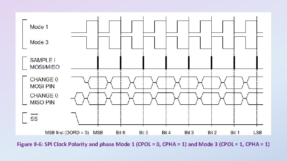
Figure 8 -6: SPI Clock Polarity and phase Mode 1 (CPOL = 0, CPHA = 1) and Mode 3 (CPOL = 1, CPHA = 1)

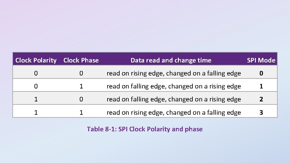
Clock Polarity Clock Phase Data read and change time SPI Mode 0 0 read on rising edge, changed on a falling edge 0 0 1 read on falling edge, changed on a rising edge 1 1 0 read on falling edge, changed on a rising edge 2 1 1 read on rising edge, changed on a falling edge 3 Table 8 -1: SPI Clock Polarity and phase

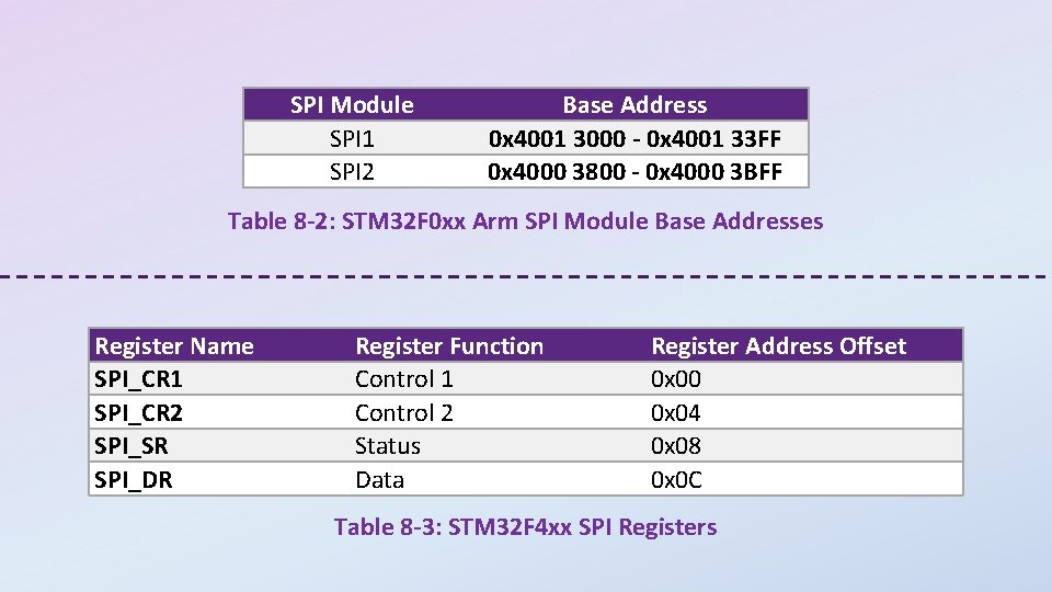
SPI Module SPI 1 SPI 2 Base Address 0 x 4001 3000 - 0 x 4001 33 FF 0 x 4000 3800 - 0 x 4000 3 BFF Table 8 -2: STM 32 F 0 xx Arm SPI Module Base Addresses Register Name SPI_CR 1 SPI_CR 2 SPI_SR SPI_DR Register Function Control 1 Control 2 Status Data Register Address Offset 0 x 00 0 x 04 0 x 08 0 x 0 C Table 8 -3: STM 32 F 4 xx SPI Registers

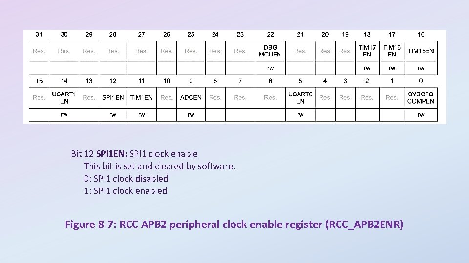
Bit 12 SPI 1 EN: SPI 1 clock enable This bit is set and cleared by software. 0: SPI 1 clock disabled 1: SPI 1 clock enabled Figure 8 -7: RCC APB 2 peripheral clock enable register (RCC_APB 2 ENR)

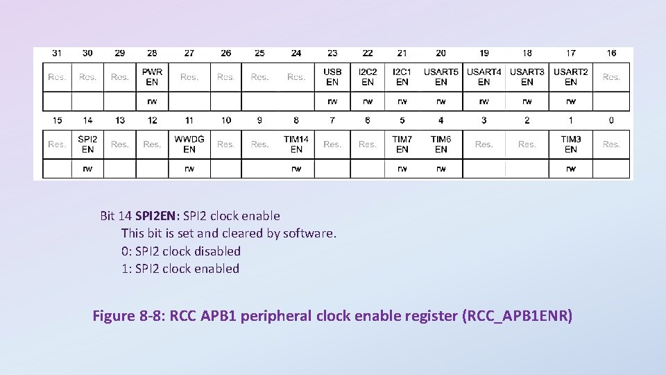
Bit 14 SPI 2 EN: SPI 2 clock enable This bit is set and cleared by software. 0: SPI 2 clock disabled 1: SPI 2 clock enabled Figure 8 -8: RCC APB 1 peripheral clock enable register (RCC_APB 1 ENR)

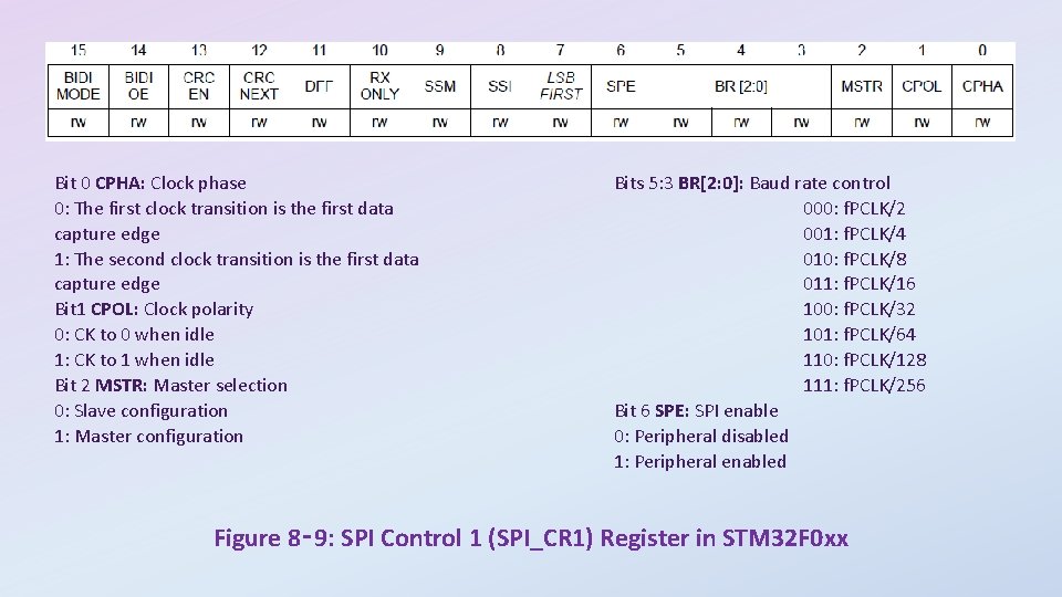
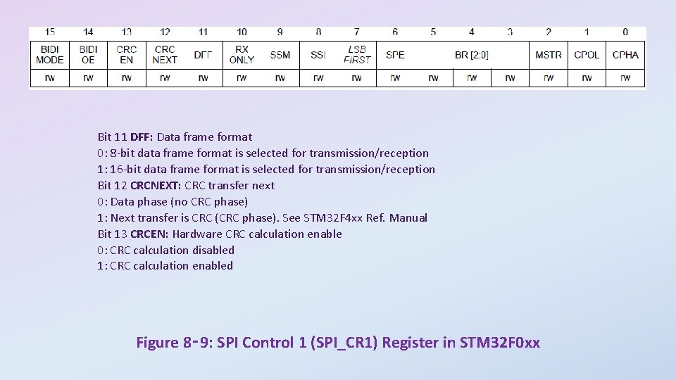
Bit 0 CPHA: Clock phase 0: The first clock transition is the first data capture edge 1: The second clock transition is the first data capture edge Bit 1 CPOL: Clock polarity 0: CK to 0 when idle 1: CK to 1 when idle Bit 2 MSTR: Master selection 0: Slave configuration 1: Master configuration Bits 5: 3 BR[2: 0]: Baud rate control 000: f. PCLK/2 001: f. PCLK/4 010: f. PCLK/8 011: f. PCLK/16 100: f. PCLK/32 101: f. PCLK/64 110: f. PCLK/128 111: f. PCLK/256 Bit 6 SPE: SPI enable 0: Peripheral disabled 1: Peripheral enabled Figure 8‑ 9: SPI Control 1 (SPI_CR 1) Register in STM 32 F 0 xx

Bit 11 DFF: Data frame format 0: 8 -bit data frame format is selected for transmission/reception 1: 16 -bit data frame format is selected for transmission/reception Bit 12 CRCNEXT: CRC transfer next 0: Data phase (no CRC phase) 1: Next transfer is CRC (CRC phase). See STM 32 F 4 xx Ref. Manual Bit 13 CRCEN: Hardware CRC calculation enable 0: CRC calculation disabled 1: CRC calculation enabled Figure 8‑ 9: SPI Control 1 (SPI_CR 1) Register in STM 32 F 0 xx

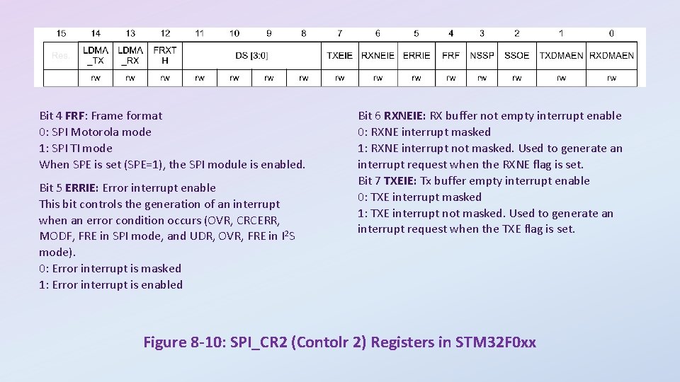
Bit 4 FRF: Frame format 0: SPI Motorola mode 1: SPI TI mode When SPE is set (SPE=1), the SPI module is enabled. Bit 5 ERRIE: Error interrupt enable This bit controls the generation of an interrupt when an error condition occurs (OVR, CRCERR, MODF, FRE in SPI mode, and UDR, OVR, FRE in I 2 S mode). 0: Error interrupt is masked 1: Error interrupt is enabled Bit 6 RXNEIE: RX buffer not empty interrupt enable 0: RXNE interrupt masked 1: RXNE interrupt not masked. Used to generate an interrupt request when the RXNE flag is set. Bit 7 TXEIE: Tx buffer empty interrupt enable 0: TXE interrupt masked 1: TXE interrupt not masked. Used to generate an interrupt request when the TXE flag is set. Figure 8 -10: SPI_CR 2 (Contolr 2) Registers in STM 32 F 0 xx
![Bits 11 8 DS 3 0 Data size These bits configure the data length Bits 11: 8 DS [3: 0]: Data size These bits configure the data length](https://slidetodoc.com/presentation_image_h2/3c694810fb430b19e93b05260e107cd7/image-15.jpg)
Bits 11: 8 DS [3: 0]: Data size These bits configure the data length for SPI transfers: 0000: Not used 1000: 9 -bit 0001: Not used 1001: 10 -bit 0010: Not used 1010: 11 -bit 0011: 4 -bit 1011: 12 -bit 0100: 5 -bit 1100: 13 -bit 0101: 6 -bit 1101: 14 -bit 0110: 7 -bit 1110: 15 -bit 0111: 8 -bit 1111: 16 -bit Figure 8 -10: SPI_CR 2 (Contolr 2) Registers in STM 32 F 0 xx

Figure 8 -11: Using STM 32 F 0 xx SPI module as Master

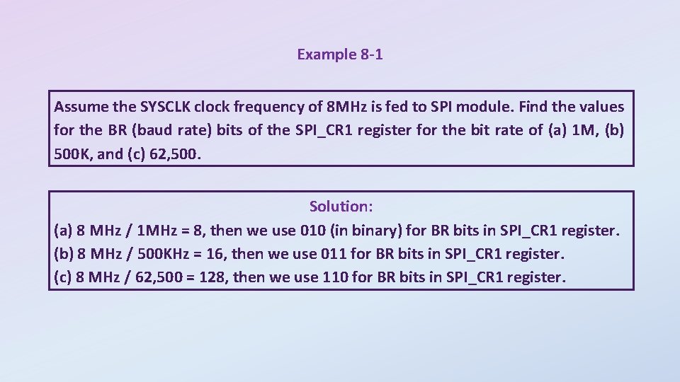
Example 8 -1 Assume the SYSCLK clock frequency of 8 MHz is fed to SPI module. Find the values for the BR (baud rate) bits of the SPI_CR 1 register for the bit rate of (a) 1 M, (b) 500 K, and (c) 62, 500. Solution: (a) 8 MHz / 1 MHz = 8, then we use 010 (in binary) for BR bits in SPI_CR 1 register. (b) 8 MHz / 500 KHz = 16, then we use 011 for BR bits in SPI_CR 1 register. (c) 8 MHz / 62, 500 = 128, then we use 110 for BR bits in SPI_CR 1 register.

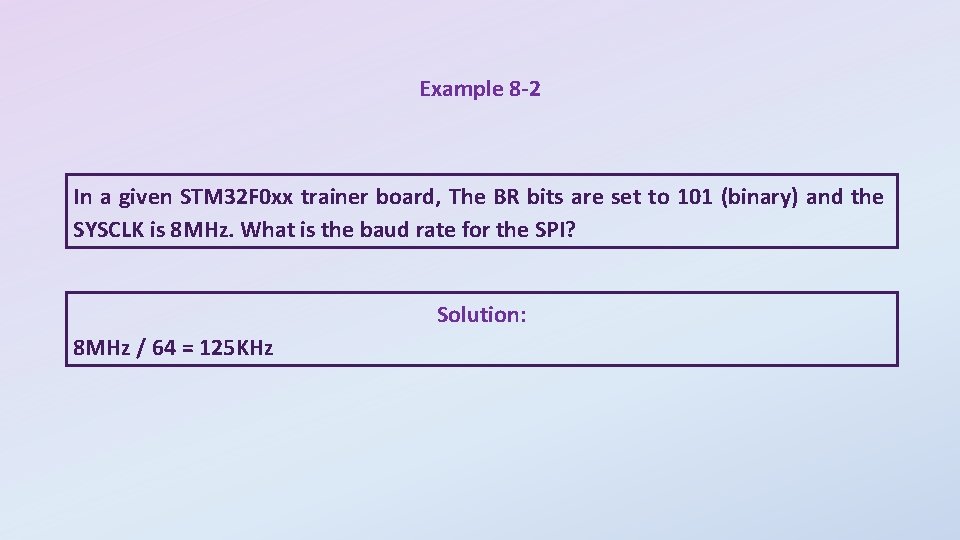
Example 8 -2 In a given STM 32 F 0 xx trainer board, The BR bits are set to 101 (binary) and the SYSCLK is 8 MHz. What is the baud rate for the SPI? Solution: 8 MHz / 64 = 125 KHz
![Bits 15 0 DR15 0 Data register Data received or to be transmitted The Bits 15: 0 DR[15: 0]: Data register Data received or to be transmitted. The](https://slidetodoc.com/presentation_image_h2/3c694810fb430b19e93b05260e107cd7/image-19.jpg)
Bits 15: 0 DR[15: 0]: Data register Data received or to be transmitted. The data register is split into 2 buffers - one for writing (Transmit Buffer) and another one for reading (Receive buffer). A write to the data register will write into the Tx buffer and a read from the data register will return the value held in the Rx buffer. Figure 8 -12: SPI_DR (Data) register Figure 8 -13: SPI_SR (Status) Register

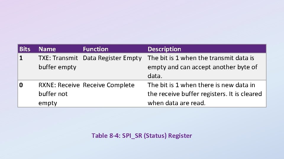
Bits 1 0 Name Function Description TXE: Transmit Data Register Empty The bit is 1 when the transmit data is buffer empty and can accept another byte of data. RXNE: Receive Complete The bit is 1 when there is new data in buffer not the receive buffer registers. It is cleared empty when data are read. Table 8 -4: SPI_SR (Status) Register

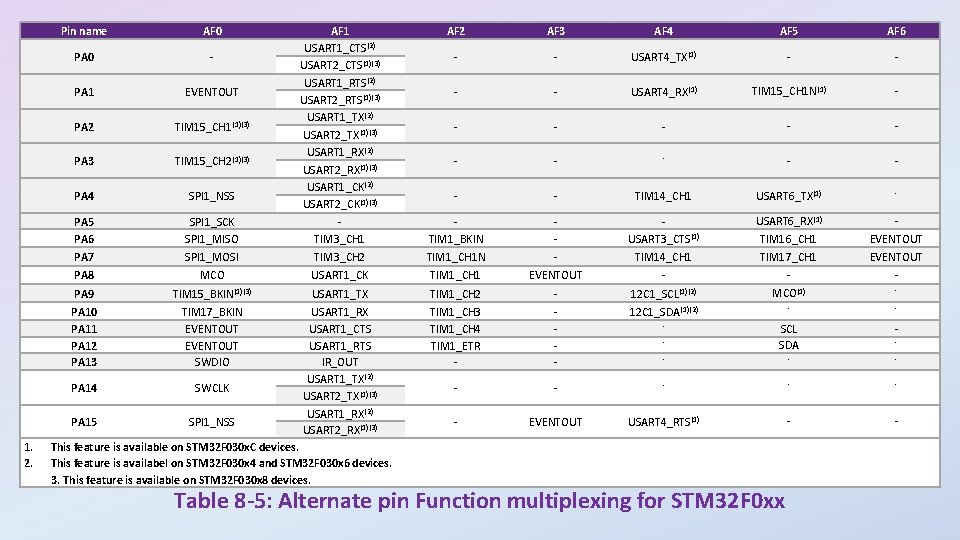
1. 2. AF 2 AF 3 AF 4 AF 5 AF 6 - - USART 4_TX(1) - - USART 4_RX(1) TIM 15_CH 1 N(1) - - - - TIM 14_CH 1 USART 6_TX(1) - TIM 1_BKIN - USART 3_CTS(1) USART 6_RX(1) TIM 16_CH 1 EVENTOUT TIM 3_CH 2 TIM 1_CH 1 N - TIM 14_CH 1 TIM 17_CH 1 EVENTOUT MCO USART 1_CK TIM 1_CH 1 EVENTOUT - - - PA 9 TIM 15_BKIN(1)(3) USART 1_TX TIM 1_CH 2 - 12 C 1_SCL(1)(2) MCO(1) - PA 10 PA 11 PA 12 PA 13 TIM 17_BKIN EVENTOUT SWDIO TIM 1_CH 3 TIM 1_CH 4 TIM 1_ETR - - 12 C 1_SDA(1)(2) - - - SCL SDA - - PA 14 SWCLK - - - PA 15 SPI 1_NSS USART 1_RX USART 1_CTS USART 1_RTS IR_OUT USART 1_TX(2) USART 2_TX(1)(3) USART 1_RX(2) USART 2_RX(1)(3) - EVENTOUT USART 4_RTS(1) - - Pin name AF 0 SPI 1_SCK SPI 1_MISO AF 1 USART 1_CTS(2) USART 2_CTS(1)(3) USART 1_RTS(2) USART 2_RTS(1)(3) USART 1_TX(2) USART 2_TX(1)(3) USART 1_RX(2) USART 2_RX(1)(3) USART 1_CK(2) USART 2_CK(1)(3) TIM 3_CH 1 PA 0 - PA 1 EVENTOUT PA 2 TIM 15_CH 1(1)(3) PA 3 TIM 15_CH 2(1)(3) PA 4 SPI 1_NSS PA 5 PA 6 PA 7 SPI 1_MOSI PA 8 This feature is available on STM 32 F 030 x. C devices. This feature is availabel on STM 32 F 030 x 4 and STM 32 F 030 x 6 devices. 3. This feature is available on STM 32 F 030 x 8 devices. - Table 8 -5: Alternate pin Function multiplexing for STM 32 F 0 xx -
![Bits 2 y 2 y1 MODERy1 0 Port x configuration bits y 0 Bits 2 y: 2 y+1 MODERy[1: 0]: Port x configuration bits (y = 0.](https://slidetodoc.com/presentation_image_h2/3c694810fb430b19e93b05260e107cd7/image-22.jpg)
Bits 2 y: 2 y+1 MODERy[1: 0]: Port x configuration bits (y = 0. . 15) These bits are written by software to configure the I/O direction mode. 00: Input (reset state) 01: General purpose output mode 10: Alternate function mode 11: Analog mode Figure 8 -14 A: GPIOx_MODER

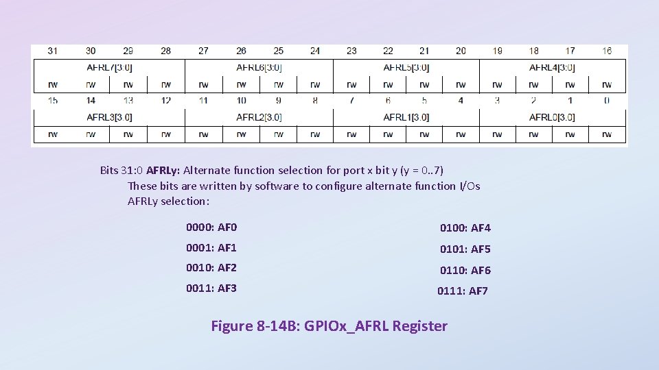
Bits 31: 0 AFRLy: Alternate function selection for port x bit y (y = 0. . 7) These bits are written by software to configure alternate function I/Os AFRLy selection: 0000: AF 0 0100: AF 4 0001: AF 1 0101: AF 5 0010: AF 2 0110: AF 6 0011: AF 3 0111: AF 7 Figure 8 -14 B: GPIOx_AFRL Register

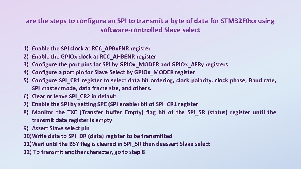
are the steps to configure an SPI to transmit a byte of data for STM 32 F 0 xx using software-controlled Slave select 1) 2) 3) 4) 5) Enable the SPI clock at RCC_APBx. ENR register Enable the GPIOx clock at RCC_AHBENR register Configure the port pins for SPI by GPIOx_MODER and GPIOx_AFRy registers Configure a port pin for Slave Select by GPIOx_MODER register Configure SPI_CR 1 register to select data bit ordering, clock polarity, clock phase, Baud rate, SPI master mode, data frame size, and others. 6) Clear or leave SPI_CR 2 in default 7) Enable the SPI by setting SPE (SPI enable) bit of SPI_CR 1 register 8) Monitor the TXE (Transfer buffer Empty) flag bit of the SPI_SR (status) register until the transmit data register is empty 9) Assert Slave select pin 10)Write data to SPI_DR (data) register to be transmitted 11)Wait until the BSY flag is cleared in SPI_SR then deassert Slave select 12) To transmit another character, go to step 8

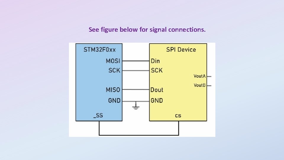
See figure below for signal connections.

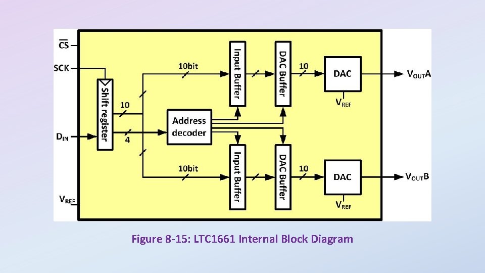
Figure 8 -15: LTC 1661 Internal Block Diagram

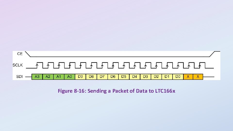
Figure 8 -16: Sending a Packet of Data to LTC 166 x

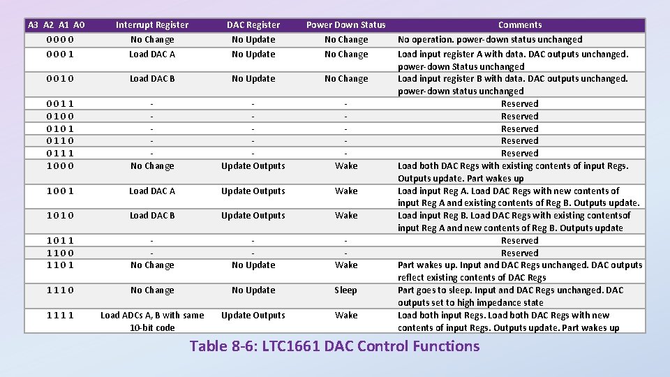
A 3 A 2 A 1 A 0 0001 Interrupt Register No Change Load DAC A DAC Register No Update Power Down Status No Change 0010 Load DAC B No Update No Change 0011 0100 0101 0110 0111 1000 No Change Update Outputs Wake 1001 Load DAC A Update Outputs Wake 1010 Load DAC B Update Outputs Wake 1011 1100 1101 No Change No Update Wake 1110 No Change No Update Sleep 1111 Load ADCs A, B with same 10 -bit code Update Outputs Wake Comments No operation. power-down status unchanged Load input register A with data. DAC outputs unchanged. power-down Status unchanged Load input register B with data. DAC outputs unchanged. power-down status unchanged Reserved Reserved Load both DAC Regs with existing contents of input Regs. Outputs update. Part wakes up Load input Reg A. Load DAC Regs with new contents of input Reg A and existing contents of Reg B. Outputs update. Load input Reg B. Load DAC Regs with existing contentsof input Reg A and new contents of Reg B. Outputs update Reserved Part wakes up. Input and DAC Regs unchanged. DAC outputs reflect existing contents of DAC Regs Part goes to sleep. Input and DAC Regs unchanged. DAC outputs set to high impedance state Load both input Regs. Load both DAC Regs with new contents of input Regs. Outputs update. Part wakes up Table 8 -6: LTC 1661 DAC Control Functions

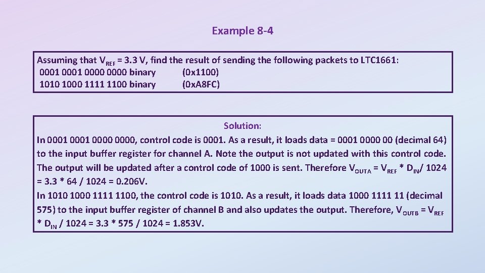
Example 8 -4 Assuming that VREF = 3. 3 V, find the result of sending the following packets to LTC 1661: 0001 0000 binary (0 x 1100) 1010 1000 1111 1100 binary (0 x. A 8 FC) Solution: In 0001 0000, control code is 0001. As a result, it loads data = 0001 0000 00 (decimal 64) to the input buffer register for channel A. Note the output is not updated with this control code. The output will be updated after a control code of 1000 is sent. Therefore VOUTA = VREF * DIN/ 1024 = 3. 3 * 64 / 1024 = 0. 206 V. In 1010 1000 1111 1100, the control code is 1010. As a result, it loads data 1000 1111 11 (decimal 575) to the input buffer register of channel B and also updates the output. Therefore, V OUTB = VREF * DIN / 1024 = 3. 3 * 575 / 1024 = 1. 853 V.

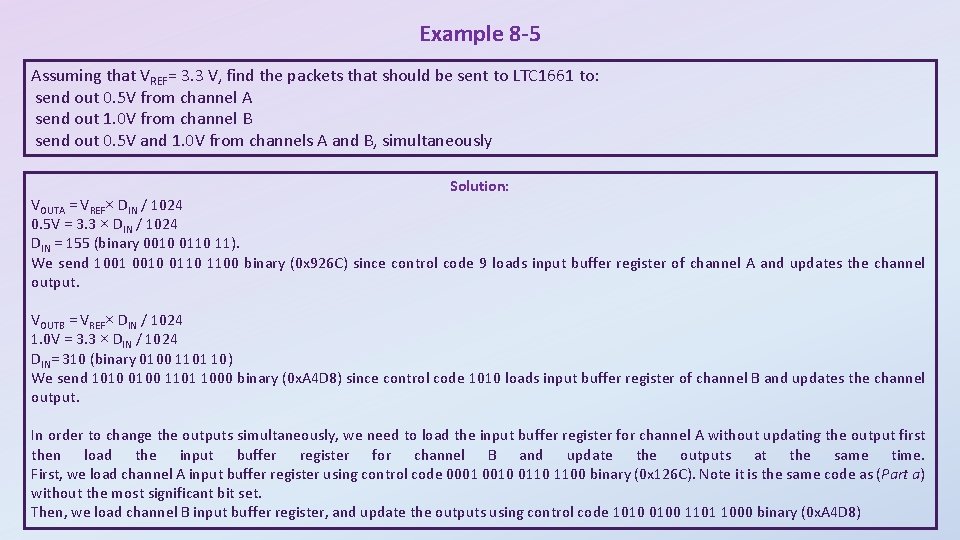
Example 8 -5 Assuming that VREF= 3. 3 V, find the packets that should be sent to LTC 1661 to: send out 0. 5 V from channel A send out 1. 0 V from channel B send out 0. 5 V and 1. 0 V from channels A and B, simultaneously Solution: VOUTA = VREF× DIN / 1024 0. 5 V = 3. 3 × DIN / 1024 DIN = 155 (binary 0010 0110 11). We send 1001 0010 0110 1100 binary (0 x 926 C) since control code 9 loads input buffer register of channel A and updates the channel output. VOUTB = VREF× DIN / 1024 1. 0 V = 3. 3 × DIN / 1024 DIN= 310 (binary 0100 1101 10) We send 1010 0100 1101 1000 binary (0 x. A 4 D 8) since control code 1010 loads input buffer register of channel B and updates the channel output. In order to change the outputs simultaneously, we need to load the input buffer register for channel A without updating the output first then load the input buffer register for channel B and update the outputs at the same time. First, we load channel A input buffer register using control code 0001 0010 0110 1100 binary (0 x 126 C). Note it is the same code as (Part a) without the most significant bit set. Then, we load channel B input buffer register, and update the outputs using control code 1010 0100 1101 1000 binary (0 x. A 4 D 8)

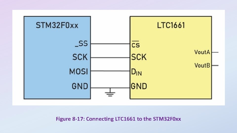
Figure 8 -17: Connecting LTC 1661 to the STM 32 F 0 xx

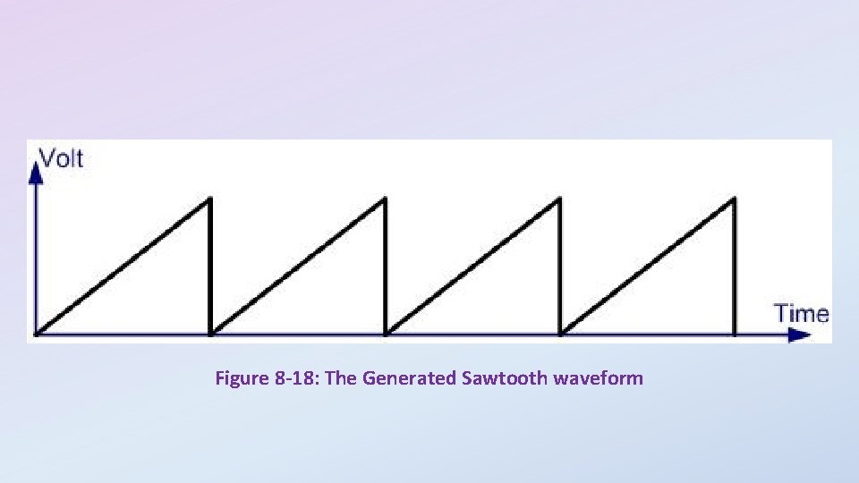
Figure 8 -18: The Generated Sawtooth waveform