Chapter 8 SPI Protocol and DAC Interfacing 1
- Slides: 27

Chapter 8 SPI Protocol and DAC Interfacing 1

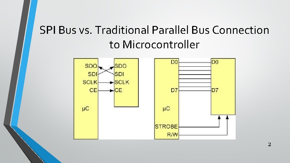
SPI Bus vs. Traditional Parallel Bus Connection to Microcontroller 2

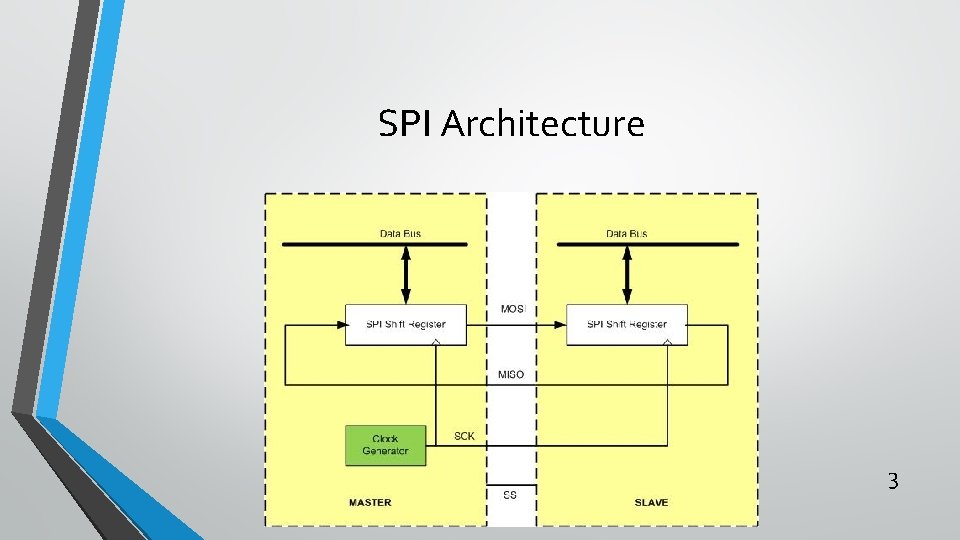
SPI Architecture 3

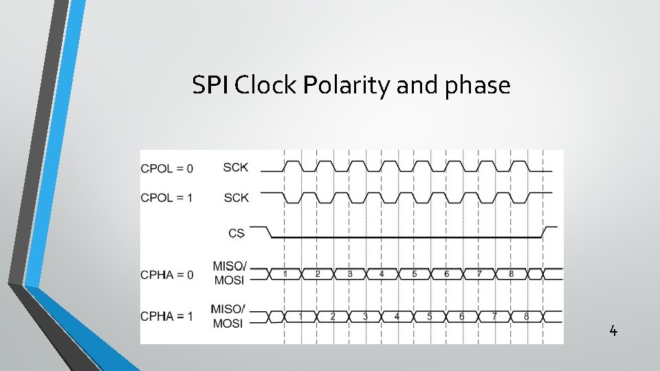
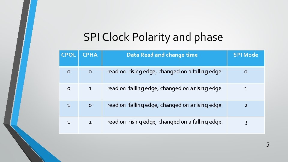
SPI Clock Polarity and phase 4

SPI Clock Polarity and phase CPOL CPHA Data Read and change time SPI Mode 0 0 read on rising edge, changed on a falling edge 0 0 1 read on falling edge, changed on a rising edge 1 1 0 read on falling edge, changed on a rising edge 2 1 1 read on rising edge, changed on a falling edge 3 5

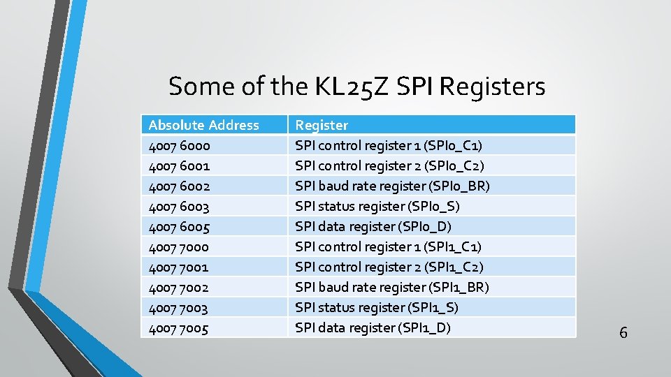
Some of the KL 25 Z SPI Registers Absolute Address 4007 6000 4007 6001 4007 6002 4007 6003 4007 6005 4007 7000 4007 7001 4007 7002 4007 7003 4007 7005 Register SPI control register 1 (SPI 0_C 1) SPI control register 2 (SPI 0_C 2) SPI baud rate register (SPI 0_BR) SPI status register (SPI 0_S) SPI data register (SPI 0_D) SPI control register 1 (SPI 1_C 1) SPI control register 2 (SPI 1_C 2) SPI baud rate register (SPI 1_BR) SPI status register (SPI 1_S) SPI data register (SPI 1_D) 6

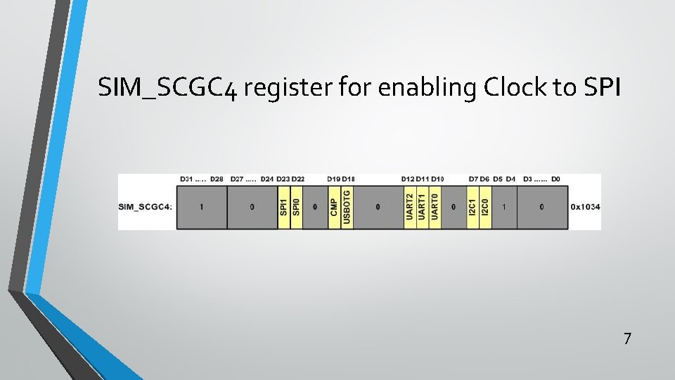
SIM_SCGC 4 register for enabling Clock to SPI 7

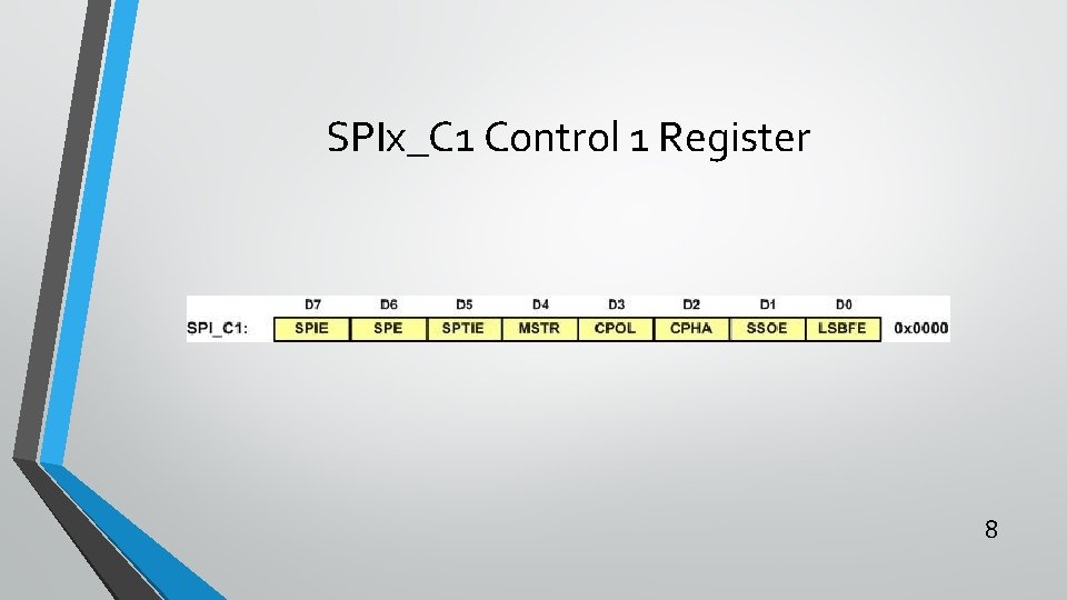
SPIx_C 1 Control 1 Register 8

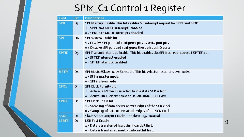
SPIx_C 1 Control 1 Register Field SPIE Bit D 7 SPE D 6 SPTIE D 5 MSTR D 4 CPOL D 3 CPHA D 2 SSOE LSBFE D 1 D 0 Descriptions SPI Interrupt Enable. This bit enables SPI interrupt request for SPRF and MODF. 1 = SPRF and MODF interrupts enabled 0 = SPRF and MODF interrupts disabled SPI System Enable bit 1 = Enables SPI port and configures pins as serial port pins 0 = Disables SPI port and configures these pins as I/O ports SPI Transmit Interrupt Enable. This bit enables the SPI interrupt request if SPTEF = 1. 1 = SPTEF interrupt enabled 0 = SPTEF interrupt disabled SPI Master/Slave mode Select bit. This bit selects master or slave mode. 1 = SPI in master mode 0 = SPI in slave mode SPI Clock Polarity bit 1 = Active-LOW clocks selected. In idle state SCK is high. 0 = Active-HIGH clocks selected. In idle state SCK is low. SPI Clock Phase bit 1 = Sampling of data occurs at even edges of the SCK clock. 0 = Sampling of data occurs at odd edges of the SCK clock. Slave Select Output Enable. See the KL 25 Z manual. LSB First Enable 1 = Data is transferred least significant bit first. 0 = Data is transferred most significant bit first. 9

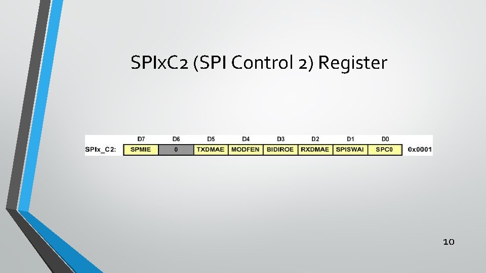
SPIx. C 2 (SPI Control 2) Register 10

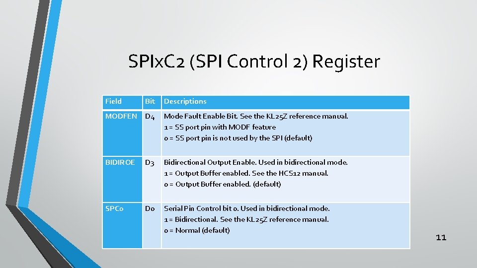
SPIx. C 2 (SPI Control 2) Register Field Bit Descriptions MODFEN D 4 Mode Fault Enable Bit. See the KL 25 Z reference manual. 1 = SS port pin with MODF feature 0 = SS port pin is not used by the SPI (default) BIDIROE D 3 Bidirectional Output Enable. Used in bidirectional mode. 1 = Output Buffer enabled. See the HCS 12 manual. 0 = Output Buffer enabled. (default) SPC 0 D 0 Serial Pin Control bit 0. Used in bidirectional mode. 1 = Bidirectional. See the KL 25 Z reference manual. 0 = Normal (default) 11

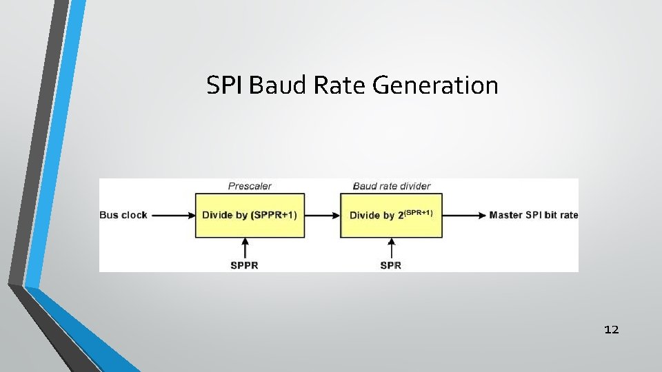
SPI Baud Rate Generation 12

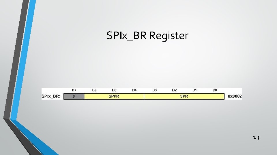
SPIx_BR Register 13

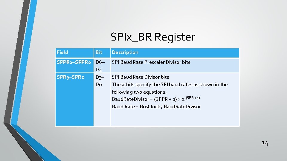
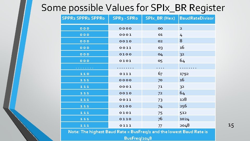
SPIx_BR Register Field Bit SPPR 2–SPPR 0 D 6– D 4 SPR 3–SPR 0 D 3– D 0 Description SPI Baud Rate Prescaler Divisor bits SPI Baud Rate Divisor bits These bits specify the SPI baud rates as shown in the following two equations: Baud. Rate. Divisor = (SPPR + 1) × 2 (SPR + 1) Baud Rate = Bus. Clock / Baud. Rate. Divisor 14

Some possible Values for SPIx_BR Register SPPR 2 SPPR 1 SPPR 0 SPR 3 - SPR 0 SPIx_BR (Hex) Baud. Rate. Divisor 000 0 0 00 2 000 0 1 01 4 000 0 0 1 0 02 8 000 0 0 1 1 03 16 000 0 1 0 0 04 32 000 0 1 05 64. . . . 110 0 1 1 1 67 1792 111 0 0 70 16 111 0 0 0 1 71 32 111 0 0 1 0 72 64 111 0 0 1 1 73 128 111 0 0 74 256 111 0 1 75 512 111 0 1 1 0 76 1024 111 0 1 1 1 77 2048 Note: The highest Baud Rate = Bus. Freq/2 and the lowest Baud Rate is Bus. Freq/2048 15

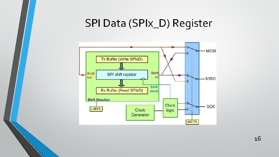
SPI Data (SPIx_D) Register 16

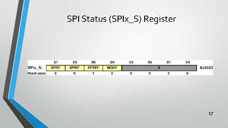
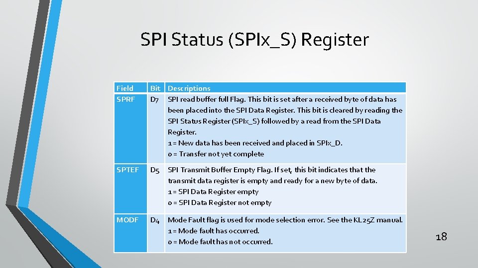
SPI Status (SPIx_S) Register 17

SPI Status (SPIx_S) Register Field SPRF Bit Descriptions D 7 SPI read buffer full Flag. This bit is set after a received byte of data has been placed into the SPI Data Register. This bit is cleared by reading the SPI Status Register (SPIx_S) followed by a read from the SPI Data Register. 1 = New data has been received and placed in SPIx_D. 0 = Transfer not yet complete SPTEF D 5 SPI Transmit Buffer Empty Flag. If set, this bit indicates that the transmit data register is empty and ready for a new byte of data. 1 = SPI Data Register empty 0 = SPI Data Register not empty MODF D 4 Mode Fault flag is used for mode selection error. See the KL 25 Z manual. 1 = Mode fault has occurred. 0 = Mode fault has not occurred. 18

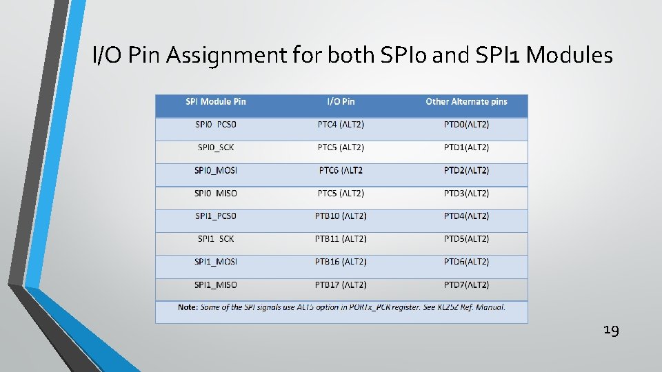
I/O Pin Assignment for both SPI 0 and SPI 1 Modules 19

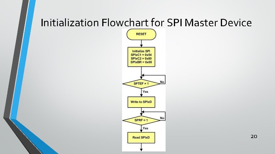
Initialization Flowchart for SPI Master Device 20

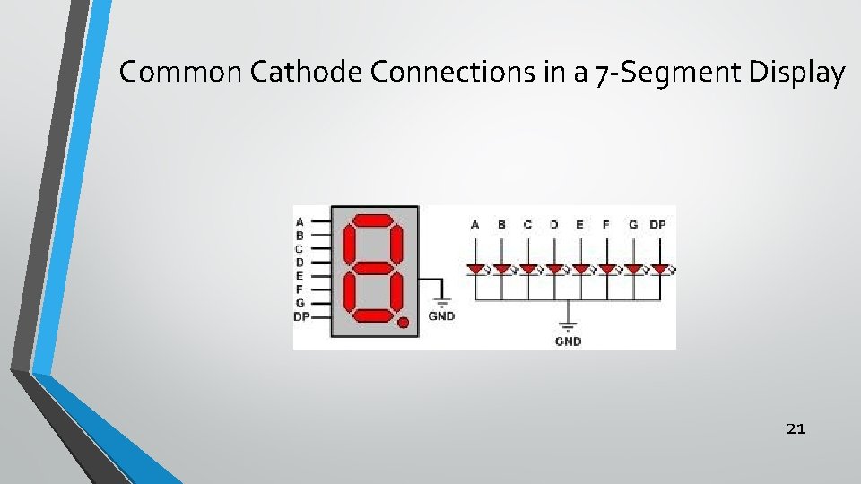
Common Cathode Connections in a 7 -Segment Display 21

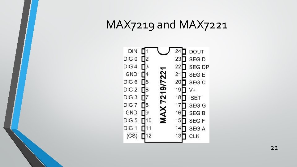
MAX 7219 and MAX 7221 22

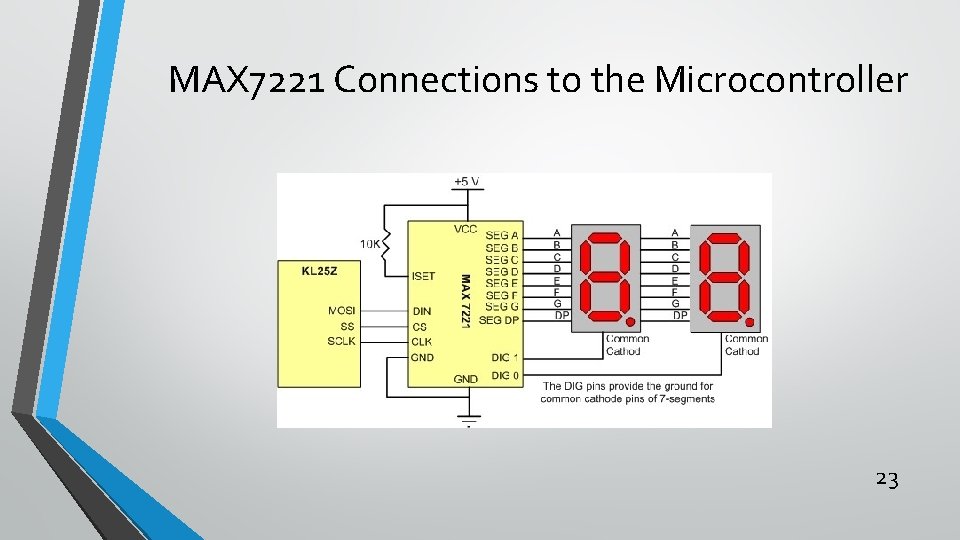
MAX 7221 Connections to the Microcontroller 23

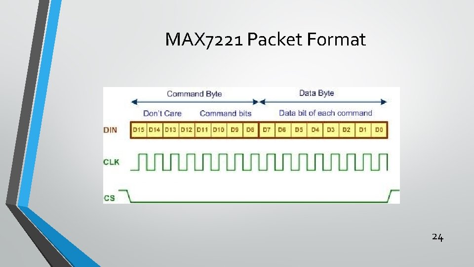
MAX 7221 Packet Format 24

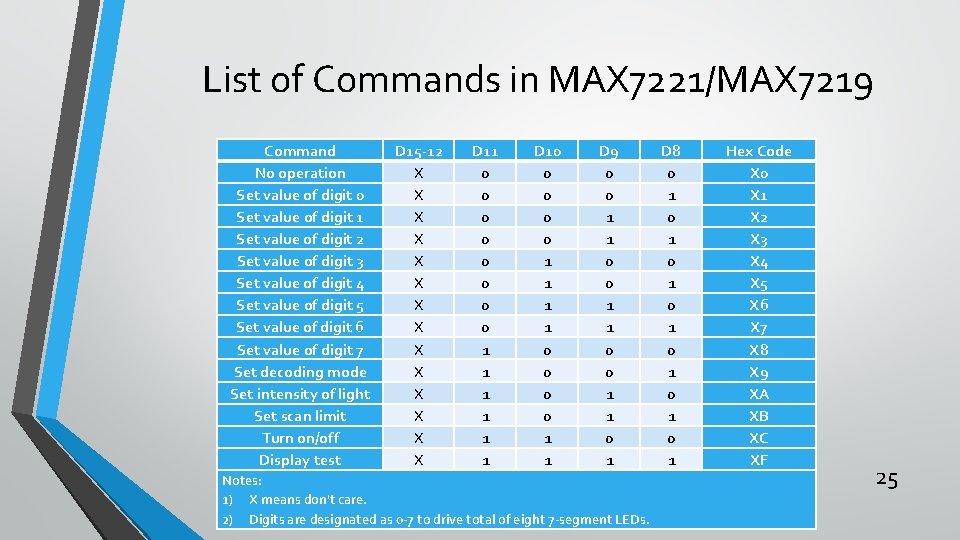
List of Commands in MAX 7221/MAX 7219 Command No operation Set value of digit 0 Set value of digit 1 Set value of digit 2 Set value of digit 3 Set value of digit 4 Set value of digit 5 Set value of digit 6 Set value of digit 7 Set decoding mode Set intensity of light Set scan limit Turn on/off Display test D 15 -12 X X X X D 11 0 0 0 0 1 1 1 D 10 0 0 1 1 D 9 0 0 1 1 0 1 Notes: 1) X means don't care. 2) Digits are designated as 0 -7 to drive total of eight 7 -segment LEDs. D 8 0 1 0 1 Hex Code X 0 X 1 X 2 X 3 X 4 X 5 X 6 X 7 X 8 X 9 XA XB XC XF 25

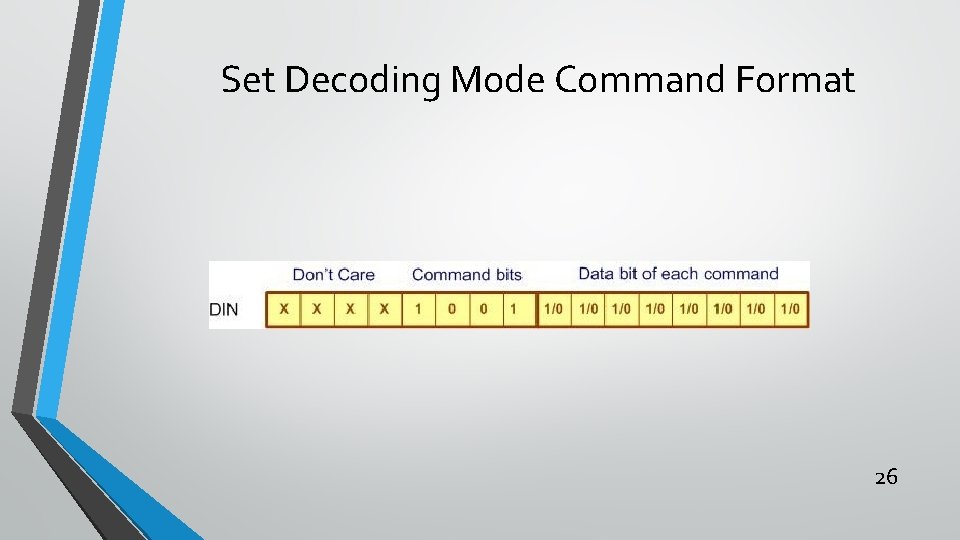
Set Decoding Mode Command Format 26

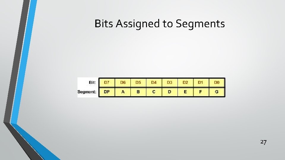
Bits Assigned to Segments 27