CHAPTER 8 Electrical Electronic Drawings Types of Drawing


- Slides: 18
CHAPTER 8 Electrical Electronic Drawings
Types of Drawing 1. 2. 3. 4. 5. Block Diagram Wiring Diagram Schematic Diagram Logic Diagram Printed Circuit Board (PCB) Drawings Main difference between electronic and mechanical drawings is – NO SCALE. Schematic, block and wiring drawings define how electronic devices work together, not what size they are. In PCB, drawings become pattern for the final parts.
Drawing Standard O Drawing Title : - Conform to ANSI/ASME Y 14. 1 -1995 or ANSI/ASME Y 14. 1 M-1995 TYPE OF DIAGRAM – TTLE O Line Thickness : O General Use – MEDIUM THICKNESS O Mechanical Connection, shielding, circuit line – MEDIUM THICKNESS O Brackets, Leader Line – THIN O For Emphasis – THICK
Diagram Types O Block Diagrams – identify the relationship between systems, groups, people, or things. O Ex: Organization Chart, to show the setup of a department, project, or company. O Ex: Flow Chart, show relationships between different events in a process O Functional block diagram shows how different parts of a system function together.
Diagram Types O Single-Line Diagram – showing single lines and graphics symbols for electric circuit or system of circuits and the component devices or parts used. O Intended to describe basic function of circuit or system O Normally includes little of the detailed information and individual-parts identification of a schematic diagram O One individual line may represent single or multiple conductors O Emphasis on the function of each stage of a device
Drawing Block Diagram O Step 1 O Sketch the basic components of the diagram in their proper sequence. Events and operations should be arranged from top to bottom, left to right, input to output, cause to effect. O Step 2 O Step 3 O Step 4
Drawing Block Diagram O Step 1 O Step 2 O Sketch connecting lines with arrowheads to define relationships and show direction of information or process flow. O Step 3 O Step 4
Drawing Block Diagram O Step 1 O Step 2 O Step 3 O Rearrange components to reduce connecting line crossover and doglegs as much as possible. O Step 4
Diagram Component CROSSOVER UNNECASSARY DOGLEG WRONG
Drawing Block Diagram O Step 1 O Step 2 O Step 3 O Step 4 O Use the resulting layout to create a finished drawing. Use consistent sizes for symbols where practical.
Schematic Drawings O Schematic Diagram – shows graphical symbols, the electrical connections and the functional relationship of the part of specific circuit. O Tracing the circuit and its functions without regards to the actual size, shape or location of the component O Symbols represent many components of electronic devices (according to ANSI Y 14. 15)
Schematic Drawings O Conventional Practices O Circuit must first be designed O Signal Path (input to output). Crossover is allowed but very minimal X (a) Y (b) O Terminals (switching symbols or numbering) O Division of Parts O Reference Designations Z (c)
Other Diagrams O Wiring and Cabling Diagrams O Show components in electrical assembly are connected. Also called cabling diagram. O Printed Circuit Boards (PCB) O Electronic devices uses circuit boards, printed on fiberglass board of 0. 06 inch thick. O Uses etching process to create traces of copper about 0. 02 inch wide and 0. 003 inch thick. O Uses computer software to construct circuit and chemicals to etch on boards. Schematic Drawing Artwork Drawing Fabrication Drawing Silkscreen Drawing Assembly Drawing
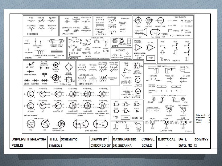
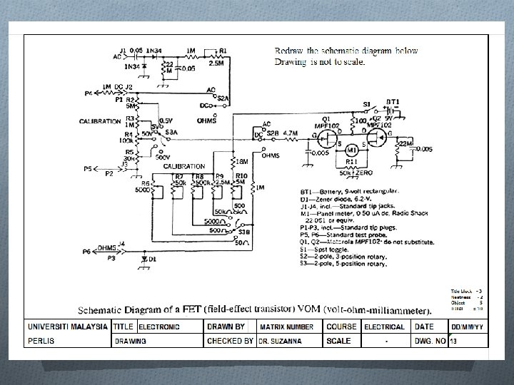
Weekly Task O Drawing No 12 and 13 O Arrange neatly all the symbols shown in Drawing No 12. O Drawing No 13 must use small letter according to standard size. O Strictly submit on Monday (G 1&G 4) or Wednesday (G 2&G 3) at the office. NO drawings will be accepted afterwards. - END OF HAND-DRAWING TASK -