Chapter 8 CPU and Memory Design Implementation and
- Slides: 38

Chapter 8 CPU and Memory: Design, Implementation, and Enhancement The Architecture of Computer Hardware and Systems Software: An Information Technology Approach 3 rd Edition, Irv Englander John Wiley and Sons 2003

CPU Architecture Overview § § § CISC – Complex Instruction Set Computer RISC – Reduced Instruction Set Computer CISC vs. RISC Comparisons VLIW – Very Long Instruction Word EPIC – Explicitly Parallel Instruction Computer Chapter 8: CPU and Memory: Design, Implementation, and Enhancement 2

CISC Architecture § Examples § Intel x 86, IBM Z-Series Mainframes, older CPU architectures § Characteristics § Few general purpose registers § Many addressing modes § Large number of specialized, complex instructions § Instructions are of varying sizes Chapter 8: CPU and Memory: Design, Implementation, and Enhancement 3

Limitations of CISC Architecture § Complex instructions are infrequently used by programmers and compilers § Memory references, loads and stores, are slow and account for a significant fraction of all instructions § Procedure and function calls are a major bottleneck § Passing arguments § Storing and retrieving values in registers Chapter 8: CPU and Memory: Design, Implementation, and Enhancement 4

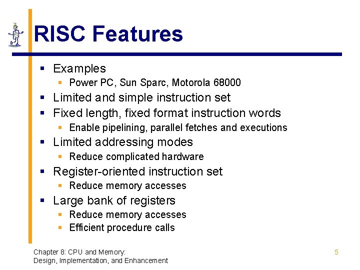
RISC Features § Examples § Power PC, Sun Sparc, Motorola 68000 § Limited and simple instruction set § Fixed length, fixed format instruction words § Enable pipelining, parallel fetches and executions § Limited addressing modes § Reduce complicated hardware § Register-oriented instruction set § Reduce memory accesses § Large bank of registers § Reduce memory accesses § Efficient procedure calls Chapter 8: CPU and Memory: Design, Implementation, and Enhancement 5

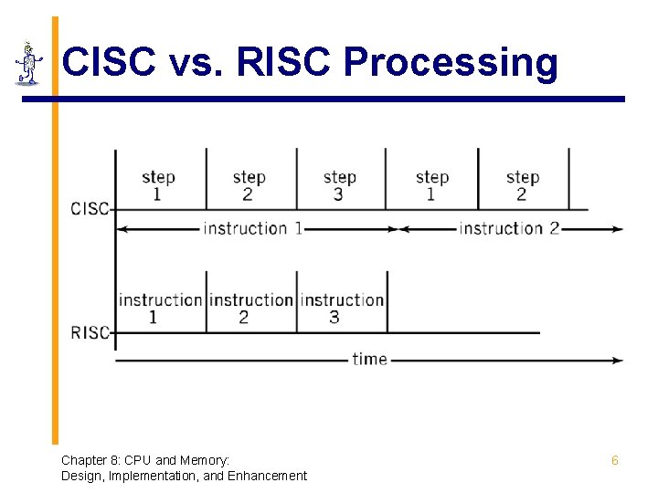
CISC vs. RISC Processing Chapter 8: CPU and Memory: Design, Implementation, and Enhancement 6

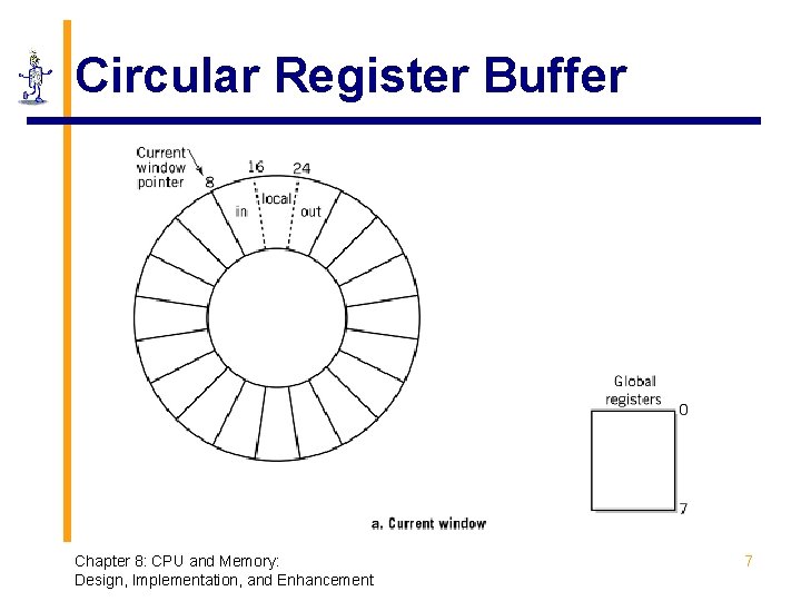
Circular Register Buffer Chapter 8: CPU and Memory: Design, Implementation, and Enhancement 7

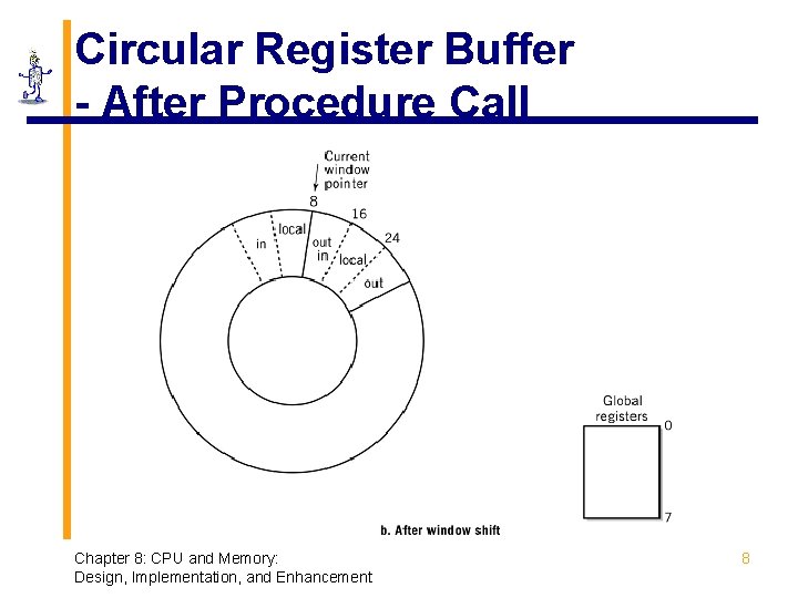
Circular Register Buffer - After Procedure Call Chapter 8: CPU and Memory: Design, Implementation, and Enhancement 8

CISC vs. RISC Performance Comparison § RISC Simpler instructions more memory accesses § RISC more bus traffic and increased cache memory misses § More registers would improve CISC performance but no space available for them § Modern CISC and RISC architectures are becoming similar Chapter 8: CPU and Memory: Design, Implementation, and Enhancement 9

VLIW Architecture § Transmeta Crusoe CPU § 128 -bit instruction bundle = molecule § 4 32 -bit atoms (atom = instruction) § Parallel processing of 4 instructions § 64 general purpose registers § Code morphing layer § Translates instructions written for other CPUs into molecules § Instructions are not written directly for the Crusoe CPU Chapter 8: CPU and Memory: Design, Implementation, and Enhancement 10

EPIC Architecture § Intel Itanium CPU § 128 -bit instruction bundle § 3 41 -bit instructions § 5 bits to identify type of instructions in bundle § § 128 64 -bit general purpose registers 128 82 -bit floating point registers Intel X 86 instruction set included Programmers and compilers follow guidelines to ensure parallel execution of instructions Chapter 8: CPU and Memory: Design, Implementation, and Enhancement 11

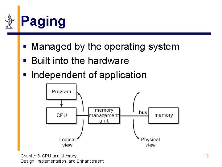
Paging § Managed by the operating system § Built into the hardware § Independent of application Chapter 8: CPU and Memory: Design, Implementation, and Enhancement 12

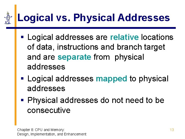
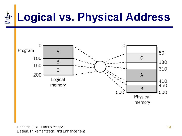
Logical vs. Physical Addresses § Logical addresses are relative locations of data, instructions and branch target and are separate from physical addresses § Logical addresses mapped to physical addresses § Physical addresses do not need to be consecutive Chapter 8: CPU and Memory: Design, Implementation, and Enhancement 13

Logical vs. Physical Address Chapter 8: CPU and Memory: Design, Implementation, and Enhancement 14

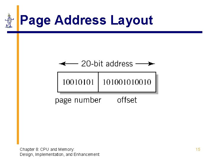
Page Address Layout Chapter 8: CPU and Memory: Design, Implementation, and Enhancement 15

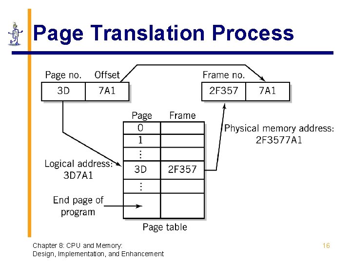
Page Translation Process Chapter 8: CPU and Memory: Design, Implementation, and Enhancement 16

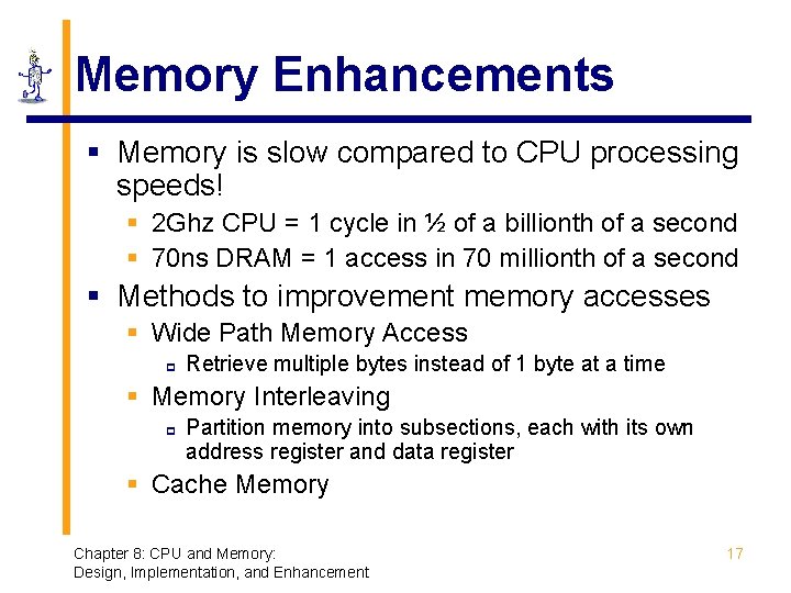
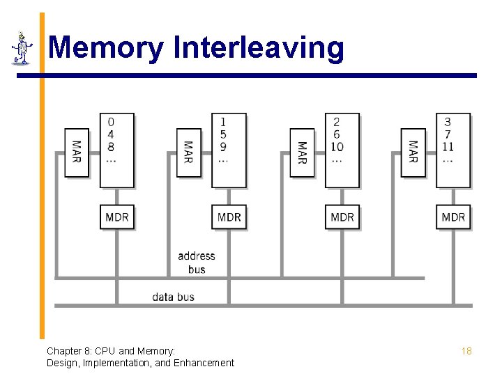
Memory Enhancements § Memory is slow compared to CPU processing speeds! § 2 Ghz CPU = 1 cycle in ½ of a billionth of a second § 70 ns DRAM = 1 access in 70 millionth of a second § Methods to improvement memory accesses § Wide Path Memory Access p Retrieve multiple bytes instead of 1 byte at a time § Memory Interleaving p Partition memory into subsections, each with its own address register and data register § Cache Memory Chapter 8: CPU and Memory: Design, Implementation, and Enhancement 17

Memory Interleaving Chapter 8: CPU and Memory: Design, Implementation, and Enhancement 18

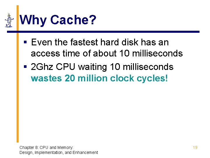
Why Cache? § Even the fastest hard disk has an access time of about 10 milliseconds § 2 Ghz CPU waiting 10 milliseconds wastes 20 million clock cycles! Chapter 8: CPU and Memory: Design, Implementation, and Enhancement 19

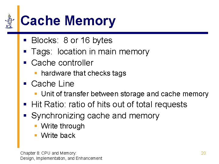
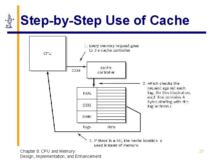
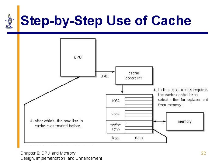
Cache Memory § Blocks: 8 or 16 bytes § Tags: location in main memory § Cache controller § hardware that checks tags § Cache Line § Unit of transfer between storage and cache memory § Hit Ratio: ratio of hits out of total requests § Synchronizing cache and memory § Write through § Write back Chapter 8: CPU and Memory: Design, Implementation, and Enhancement 20

Step-by-Step Use of Cache Chapter 8: CPU and Memory: Design, Implementation, and Enhancement 21

Step-by-Step Use of Cache Chapter 8: CPU and Memory: Design, Implementation, and Enhancement 22

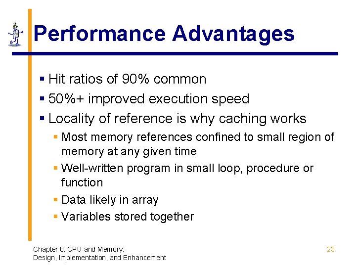
Performance Advantages § Hit ratios of 90% common § 50%+ improved execution speed § Locality of reference is why caching works § Most memory references confined to small region of memory at any given time § Well-written program in small loop, procedure or function § Data likely in array § Variables stored together Chapter 8: CPU and Memory: Design, Implementation, and Enhancement 23

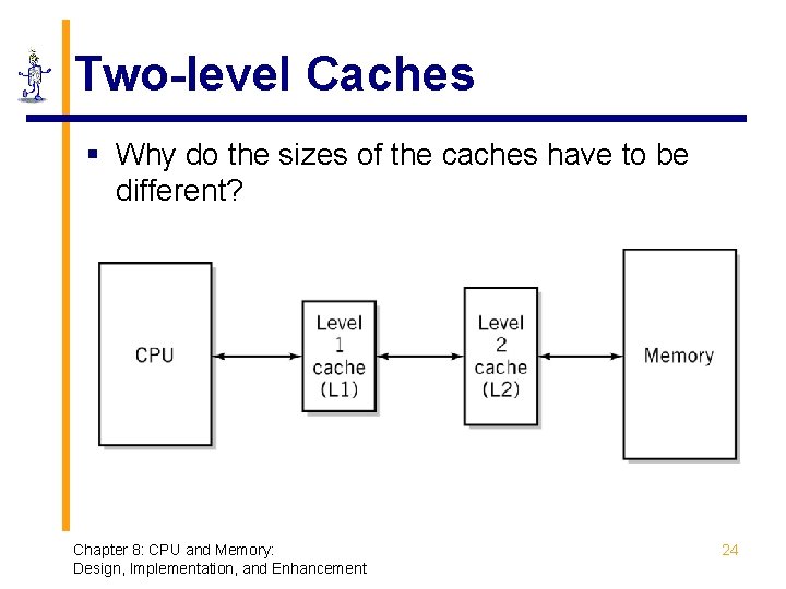
Two-level Caches § Why do the sizes of the caches have to be different? Chapter 8: CPU and Memory: Design, Implementation, and Enhancement 24

Cache vs. Virtual Memory § Cache speeds up memory access § Virtual memory increases amount of perceived storage § independence from the configuration and capacity of the memory system § low cost per bit Chapter 8: CPU and Memory: Design, Implementation, and Enhancement 25

Modern CPU Processing Methods § § § Timing Issues Separate Fetch/Execute Units Pipelining Scalar Processing Superscalar Processing Chapter 8: CPU and Memory: Design, Implementation, and Enhancement 26

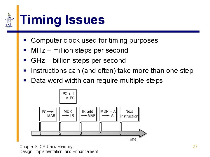
Timing Issues § § § Computer clock used for timing purposes MHz – million steps per second GHz – billion steps per second Instructions can (and often) take more than one step Data word width can require multiple steps Chapter 8: CPU and Memory: Design, Implementation, and Enhancement 27

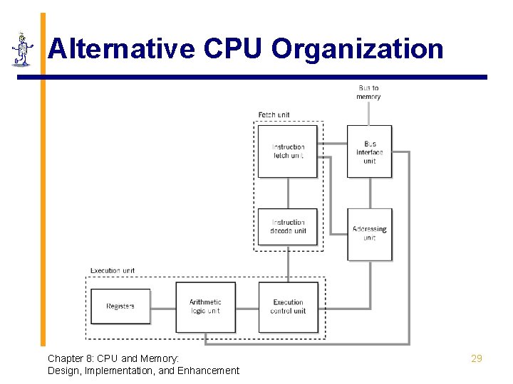
Separate Fetch-Execute Units § Fetch Unit § Instruction fetch unit § Instruction decode unit p p Determine opcode Identify type of instruction and operands § Several instructions are fetched in parallel and held in a buffer until decoded and executed § IP – Instruction Pointer register § Execute Unit § Receives instructions from the decode unit § Appropriate execution unit services the instruction Chapter 8: CPU and Memory: Design, Implementation, and Enhancement 28

Alternative CPU Organization Chapter 8: CPU and Memory: Design, Implementation, and Enhancement 29

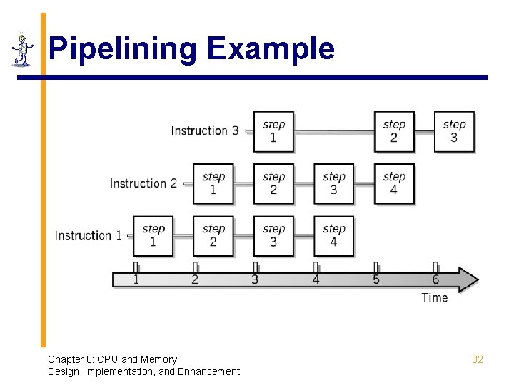
Instruction Pipelining § Assembly-line technique to allow overlapping between fetch-execute cycles of sequences of instructions § Only one instruction is being executed to completion at a time § Scalar processing § Average instruction execution is approximately equal to the clock speed of the CPU § Problems from stalling § Instructions have different numbers of steps § Problems from branching Chapter 8: CPU and Memory: Design, Implementation, and Enhancement 30

Branch Problem Solutions § Separate pipelines for both possibilities § Probabilistic approach § Requiring the following instruction to not be dependent on the branch § Instruction Reordering (superscalar processing) Chapter 8: CPU and Memory: Design, Implementation, and Enhancement 31

Pipelining Example Chapter 8: CPU and Memory: Design, Implementation, and Enhancement 32

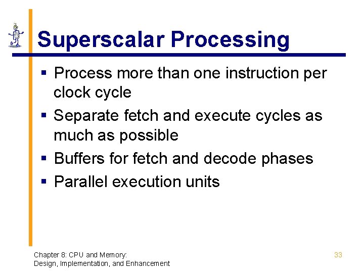
Superscalar Processing § Process more than one instruction per clock cycle § Separate fetch and execute cycles as much as possible § Buffers for fetch and decode phases § Parallel execution units Chapter 8: CPU and Memory: Design, Implementation, and Enhancement 33

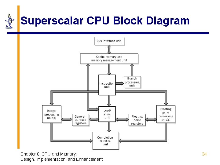
Superscalar CPU Block Diagram Chapter 8: CPU and Memory: Design, Implementation, and Enhancement 34

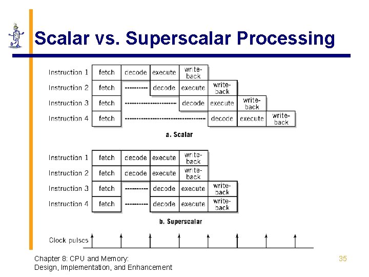
Scalar vs. Superscalar Processing Chapter 8: CPU and Memory: Design, Implementation, and Enhancement 35

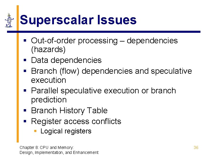
Superscalar Issues § Out-of-order processing – dependencies (hazards) § Data dependencies § Branch (flow) dependencies and speculative execution § Parallel speculative execution or branch prediction § Branch History Table § Register access conflicts § Logical registers Chapter 8: CPU and Memory: Design, Implementation, and Enhancement 36

Hardware Implementation § Hardware – operations are implemented by logic gates § Advantages § Speed § RISC designs are simple and typically implemented in hardware Chapter 8: CPU and Memory: Design, Implementation, and Enhancement 37

Microprogrammed Implementation § Microcode are tiny programs stored in ROM that replace CPU instructions § Advantages § More flexible § Easier to implement complex instructions § Can emulate other CPUs § Disadvantage § Requires more clock cycles Chapter 8: CPU and Memory: Design, Implementation, and Enhancement 38