Chapter 8 Counters By Taweesak Reungpeerakul 241 208
Chapter 8 Counters By Taweesak Reungpeerakul 241 -208 CH 8 1
Contents n n n n n 241 -208 CH 8 Introduction Asynchronous Counter Synchronous Counter Up/Down Synchronous Counters Design of Synchronous Counters Cascaded Counters Counter Decoding Counter Applications Conclusions 2
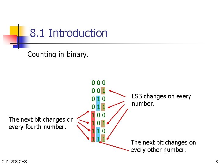
8. 1 Introduction Counting in binary. The next bit changes on every fourth number. 241 -208 CH 8 0 0 1 1 0 1 0 1 LSB changes on every number. The next bit changes on every other number. 3
8. 1 Introduction (cont. ) Counter can be formed by connecting FFs together Counter can be categorized into two cases, according to the ways they are clocked !! • Asynchronous counter (ripple counter) Each FF formed counter do not change their states at the same time • Synchronous counter Each FF in this counter is clocked concurrently. 241 -208 CH 8 4
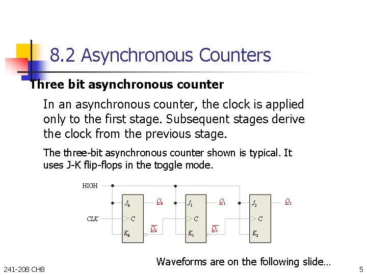
8. 2 Asynchronous Counters Three bit asynchronous counter In an asynchronous counter, the clock is applied only to the first stage. Subsequent stages derive the clock from the previous stage. The three-bit asynchronous counter shown is typical. It uses J-K flip-flops in the toggle mode. HIGH Q 0 J 0 CLK C K 0 241 -208 CH 8 Q 1 J 1 C Q 0 K 1 Q 2 J 2 C Q 1 K 2 Waveforms are on the following slide… 5
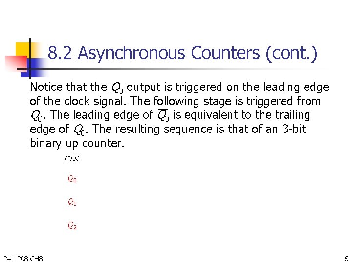
8. 2 Asynchronous Counters (cont. ) Notice that the Q 0 output is triggered on the leading edge of the clock signal. The following stage is triggered from Q 0. The leading edge of Q 0 is equivalent to the trailing edge of Q 0. The resulting sequence is that of an 3 -bit binary up counter. CLK Q 0 Q 1 Q 2 241 -208 CH 8 6
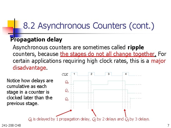
8. 2 Asynchronous Counters (cont. ) Propagation delay Asynchronous counters are sometimes called ripple counters, because the stages do not all change together. For certain applications requiring high clock rates, this is a major disadvantage. CLK Notice how delays are cumulative as each stage in a counter is clocked later than the previous stage. Q 0 Q 1 Q 2 Q 0 is delayed by 1 propagation delay, Q 2 by 2 delays and Q 3 by 3 delays. 241 -208 CH 8 7
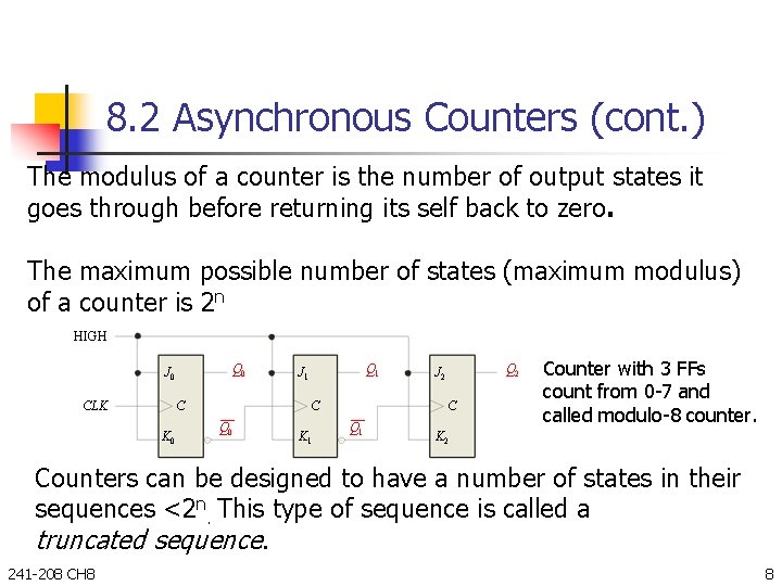
8. 2 Asynchronous Counters (cont. ) The modulus of a counter is the number of output states it goes through before returning its self back to zero. The maximum possible number of states (maximum modulus) of a counter is 2 n HIGH Q 0 J 0 CLK C K 0 Q 1 J 1 C Q 0 K 1 Q 2 J 2 C Q 1 Counter with 3 FFs count from 0 -7 and called modulo-8 counter. K 2 Counters can be designed to have a number of states in their sequences <2 n. This type of sequence is called a truncated sequence. 241 -208 CH 8 8
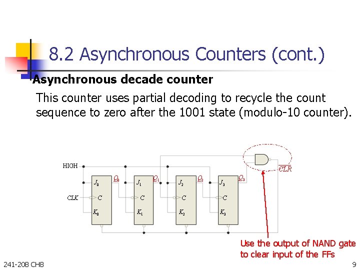
8. 2 Asynchronous Counters (cont. ) Asynchronous decade counter This counter uses partial decoding to recycle the count sequence to zero after the 1001 state (modulo-10 counter). HIGH CLR J 0 CLK C K 0 Q 0 J 1 Q 1 J 2 Q 2 J 3 C C C K 1 K 2 K 3 Q 3 Use the output of NAND gate to clear input of the FFs 241 -208 CH 8 9
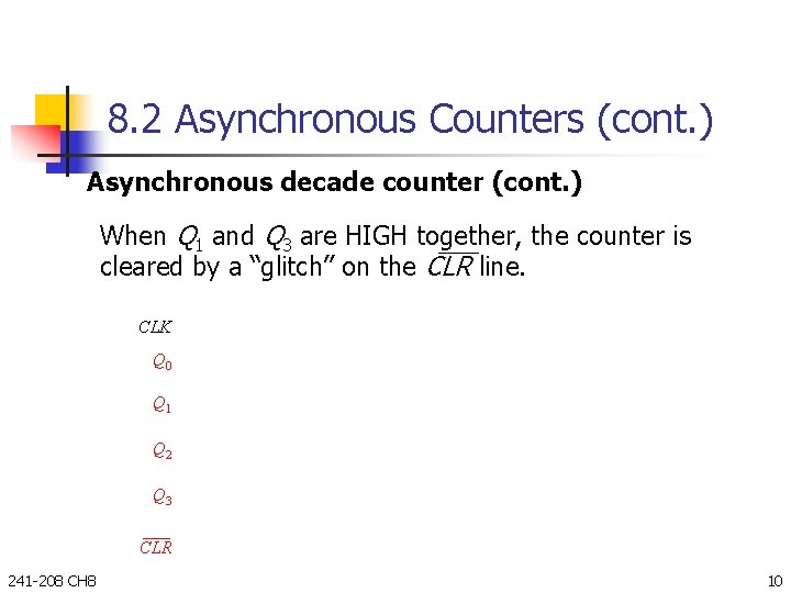
8. 2 Asynchronous Counters (cont. ) Asynchronous decade counter (cont. ) When Q 1 and Q 3 are HIGH together, the counter is cleared by a “glitch” on the CLR line. CLK Q 0 Q 1 Glitch Q 2 Q 3 CLR 241 -208 CH 8 Glitch 10
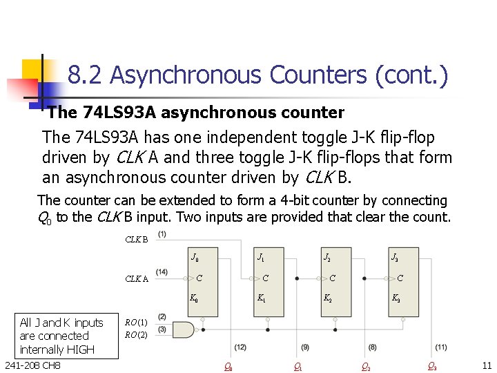
8. 2 Asynchronous Counters (cont. ) The 74 LS 93 A asynchronous counter The 74 LS 93 A has one independent toggle J-K flip-flop driven by CLK A and three toggle J-K flip-flops that form an asynchronous counter driven by CLK B. The counter can be extended to form a 4 -bit counter by connecting Q 0 to the CLK B input. Two inputs are provided that clear the count. CLK B J 0 CLK A J 1 C K 0 All J and K inputs are connected internally HIGH 241 -208 CH 8 J 2 J 3 C C C K 1 K 2 K 3 RO (1) RO (2) Q 0 Q 1 Q 2 Q 3 11
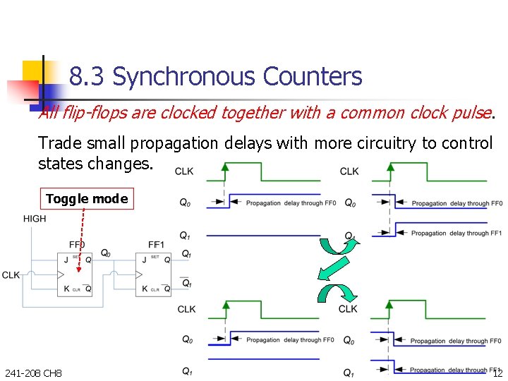
8. 3 Synchronous Counters All flip-flops are clocked together with a common clock pulse. Trade small propagation delays with more circuitry to control states changes. Toggle mode 241 -208 CH 8 12
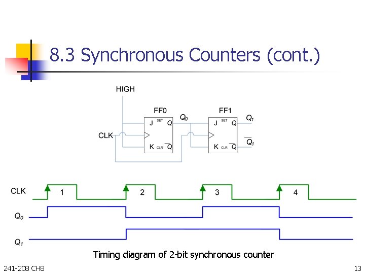
8. 3 Synchronous Counters (cont. ) Timing diagram of 2 -bit synchronous counter 241 -208 CH 8 13
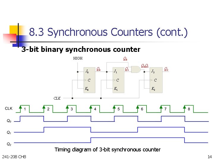
8. 3 Synchronous Counters (cont. ) 3 -bit binary synchronous counter HIGH Q 0 J 0 C K 0 Q 0 J 1 Q 0 Q 1 J 2 C C K 1 K 2 Q 2 CLK Timing diagram of 3 -bit synchronous counter 241 -208 CH 8 14
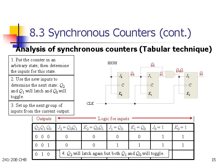
8. 3 Synchronous Counters (cont. ) Analysis of synchronous counters (Tabular technique) 1. Put the counter in an arbitrary state; then determine the inputs for this state. HIGH J 0 2. Use the new inputs to determine the next state: Q 2 and Q 1 will latch and Q 0 will toggle. 3. Set up the next group of inputs from the current output. Q 0 Q 1 J 1 C K 0 Q 0 Q 1 J 2 C C K 1 K 2 Logic for inputs Q 2 Q 1 Q 0 J 2 = Q 0 Q 1 K 2 = Q 0 Q 1 0 0 0 0 1 1 0 1 0 Q 2 CLK Outputs 241 -208 CH 8 Q 0 J 1 = Q 0 K 1 = Q 0 J 0 = 1 4. Q 2 will latch again but both Q 1 and Q 0 will toggle. K 0 = 1 15
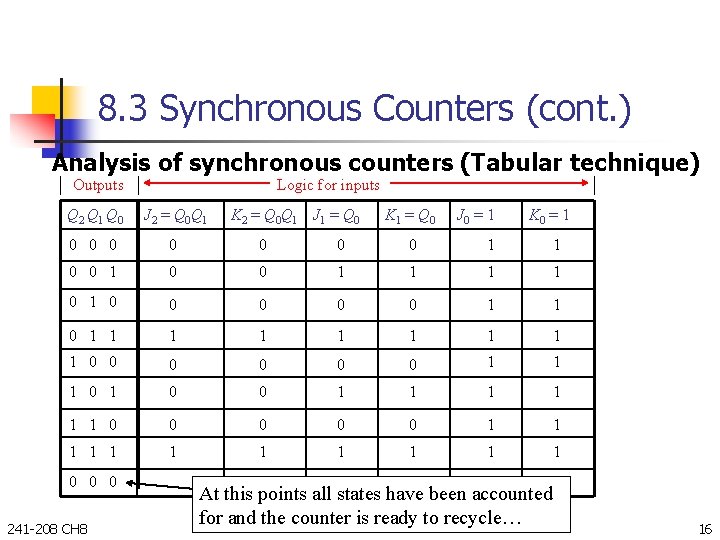
8. 3 Synchronous Counters (cont. ) Analysis of synchronous counters (Tabular technique) Outputs Logic for inputs Q 2 Q 1 Q 0 J 2 = Q 0 Q 1 0 0 0 0 1 1 0 1 0 0 0 1 1 1 0 0 0 1 1 1 0 0 0 1 1 1 0 0 0 241 -208 CH 8 K 2 = Q 0 Q 1 J 1 = Q 0 K 1 = Q 0 J 0 = 1 K 0 = 1 At this points all states have been accounted for and the counter is ready to recycle… 16
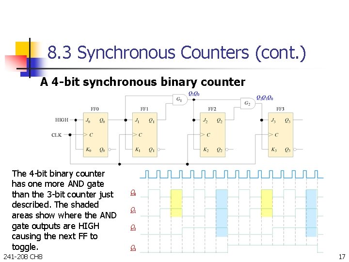
8. 3 Synchronous Counters (cont. ) A 4 -bit synchronous binary counter The 4 -bit binary counter has one more AND gate than the 3 -bit counter just described. The shaded areas show where the AND gate outputs are HIGH causing the next FF to toggle. 241 -208 CH 8 Q 0 Q 1 Q 2 Q 3 17
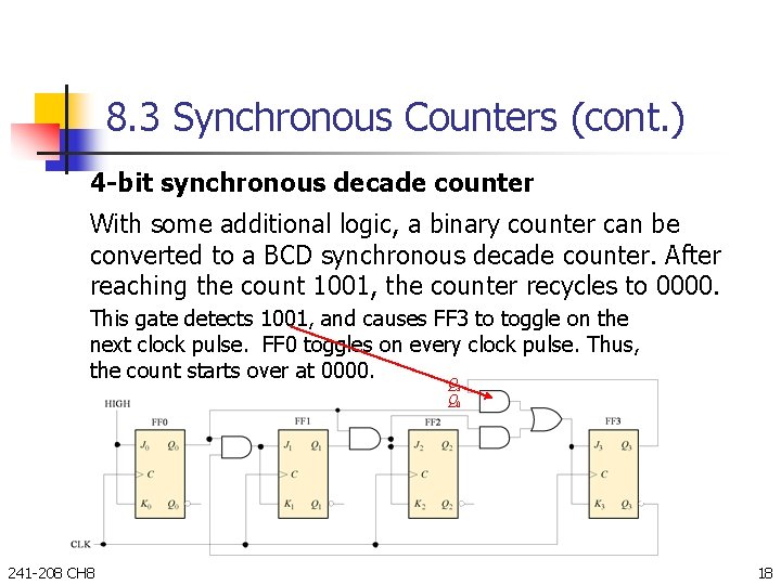
8. 3 Synchronous Counters (cont. ) 4 -bit synchronous decade counter With some additional logic, a binary counter can be converted to a BCD synchronous decade counter. After reaching the count 1001, the counter recycles to 0000. This gate detects 1001, and causes FF 3 to toggle on the next clock pulse. FF 0 toggles on every clock pulse. Thus, the count starts over at 0000. Q 3 Q 0 241 -208 CH 8 18
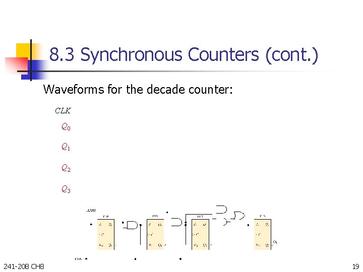
8. 3 Synchronous Counters (cont. ) Waveforms for the decade counter: CLK Q 0 Q 1 Q 2 Q 3 241 -208 CH 8 19
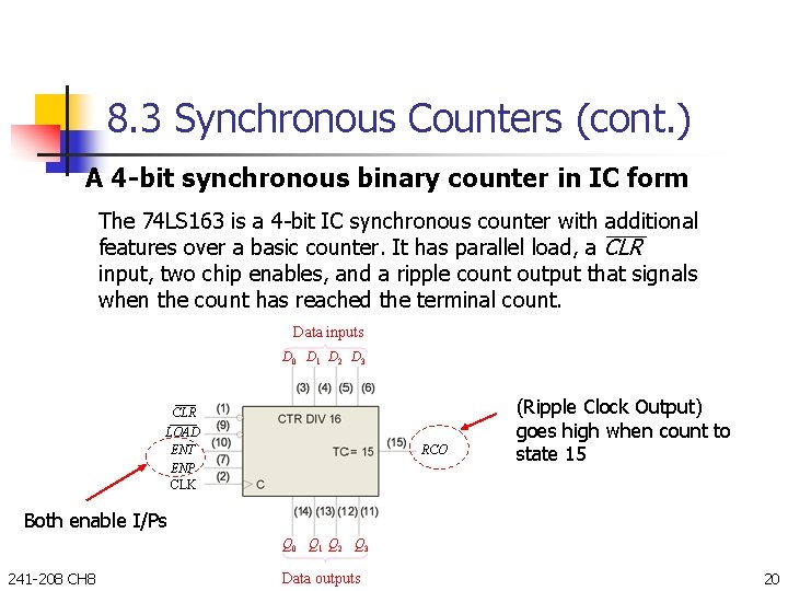
8. 3 Synchronous Counters (cont. ) A 4 -bit synchronous binary counter in IC form The 74 LS 163 is a 4 -bit IC synchronous counter with additional features over a basic counter. It has parallel load, a CLR input, two chip enables, and a ripple count output that signals when the count has reached the terminal count. Data inputs D 0 D 1 D 2 D 3 CLR LOAD ENT ENP CLK RCO (Ripple Clock Output) goes high when count to state 15 Both enable I/Ps Q 0 Q 1 Q 2 Q 3 241 -208 CH 8 Data outputs 20
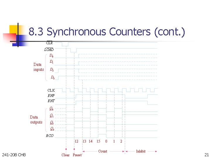
8. 3 Synchronous Counters (cont. ) CLR LOAD D 0 Data inputs D 1 D 2 D 3 CLK ENP ENT Q 0 Data outputs Q 1 Q 2 Q 3 RCO 12 241 -208 CH 8 Clear Preset 13 14 15 0 Count 1 2 Inhibit 21
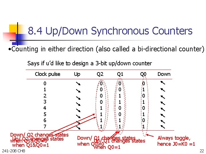
8. 4 Up/Down Synchronous Counters • Counting in either direction (also called a bi-directional counter) Says if u’d like to design a 3 -bit up/down counter Clock pulse 0 1 2 3 4 5 6 7 Down/ Q 2 changes states Up/ Q 2 changes states when Q 1&Q 0=0 when Q 1&Q 0=1 241 -208 CH 8 Up Q 2 Q 1 Q 0 0 0 1 1 0 1 0 1 Down/ Q 1 changes states Up/ Q 1 changes states when Q 0=0 when Q 0=1 Down Always toggle, hence J 0=K 0 =1 22
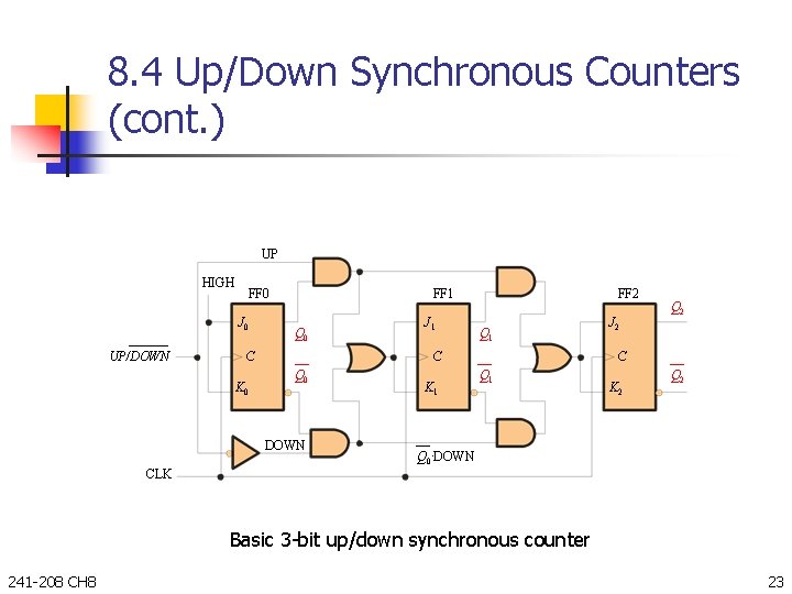
8. 4 Up/Down Synchronous Counters (cont. ) UP HIGH FF 0 J 0 UP/DOWN FF 1 Q 0 C K 0 J 1 FF 2 Q 1 C Q 0 DOWN K 1 J 2 Q 2 C Q 1 K 2 Q 0. DOWN CLK Basic 3 -bit up/down synchronous counter 241 -208 CH 8 23
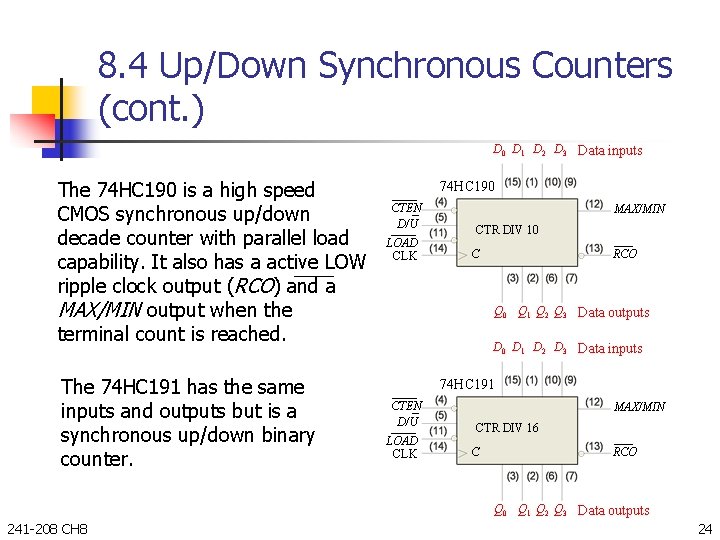
8. 4 Up/Down Synchronous Counters (cont. ) D 0 D 1 D 2 D 3 Data inputs The 74 HC 190 is a high speed CMOS synchronous up/down decade counter with parallel load capability. It also has a active LOW ripple clock output (RCO) and a MAX/MIN output when the terminal count is reached. The 74 HC 191 has the same inputs and outputs but is a synchronous up/down binary counter. 74 HC 190 CTEN D/U LOAD CLK MAX/MIN CTR DIV 10 RCO C Q 0 Q 1 Q 2 Q 3 Data outputs D 0 D 1 D 2 D 3 Data inputs 74 HC 191 CTEN D/U LOAD CLK MAX/MIN CTR DIV 16 C RCO Q 0 Q 1 Q 2 Q 3 Data outputs 241 -208 CH 8 24
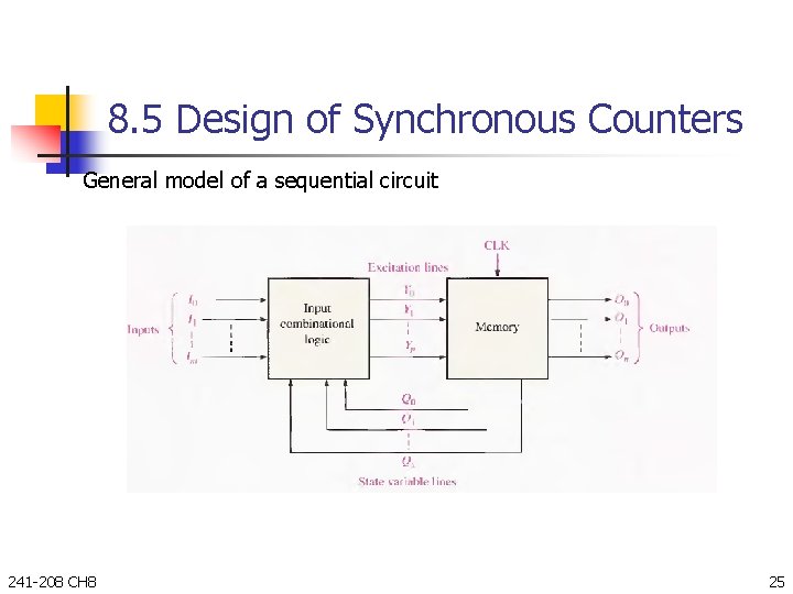
8. 5 Design of Synchronous Counters General model of a sequential circuit 241 -208 CH 8 25
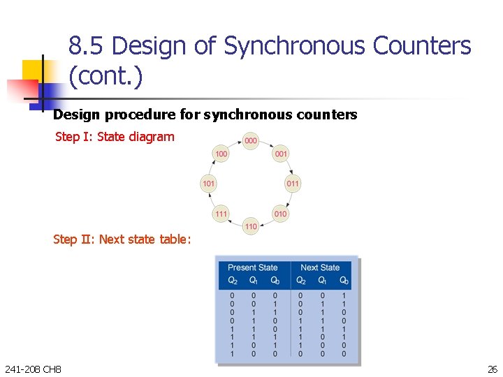
8. 5 Design of Synchronous Counters (cont. ) Design procedure for synchronous counters Step I: State diagram Step II: Next state table: 241 -208 CH 8 26
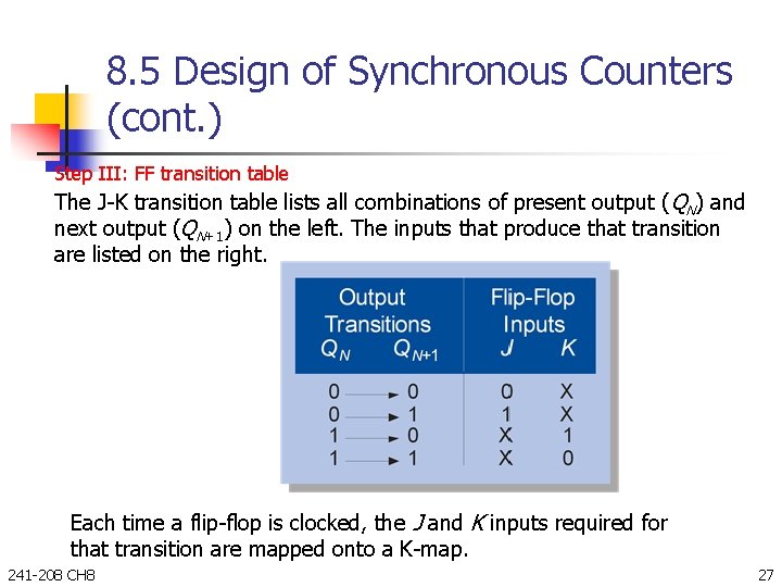
8. 5 Design of Synchronous Counters (cont. ) Step III: FF transition table The J-K transition table lists all combinations of present output ( QN) and next output (QN+1) on the left. The inputs that produce that transition are listed on the right. Each time a flip-flop is clocked, the J and K inputs required for that transition are mapped onto a K-map. 241 -208 CH 8 27
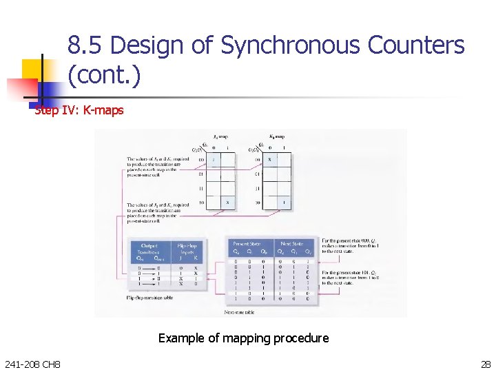
8. 5 Design of Synchronous Counters (cont. ) Step IV: K-maps Example of mapping procedure 241 -208 CH 8 28
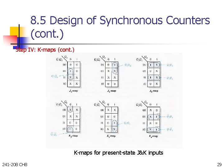
8. 5 Design of Synchronous Counters (cont. ) Step IV: K-maps (cont. ) K-maps for present-state J&K inputs 241 -208 CH 8 29
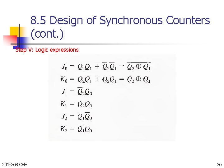
8. 5 Design of Synchronous Counters (cont. ) Step V: Logic expressions 241 -208 CH 8 30
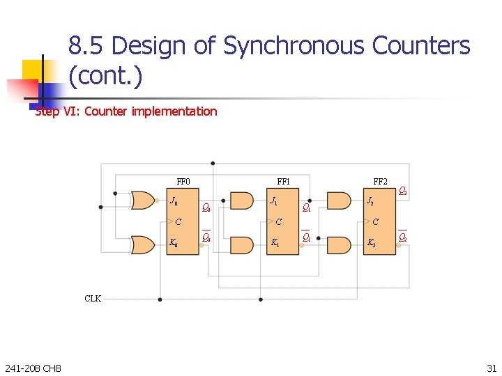
8. 5 Design of Synchronous Counters (cont. ) Step VI: Counter implementation FF 0 J 0 FF 1 Q 0 C K 0 J 1 FF 2 Q 1 C Q 0 K 1 J 2 Q 2 C Q 1 K 2 Q 2 CLK 241 -208 CH 8 31
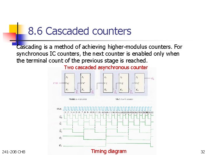
8. 6 Cascaded counters Cascading is a method of achieving higher-modulus counters. For synchronous IC counters, the next counter is enabled only when the terminal count of the previous stage is reached. Two cascaded asynchronous counter 241 -208 CH 8 Timing diagram 32
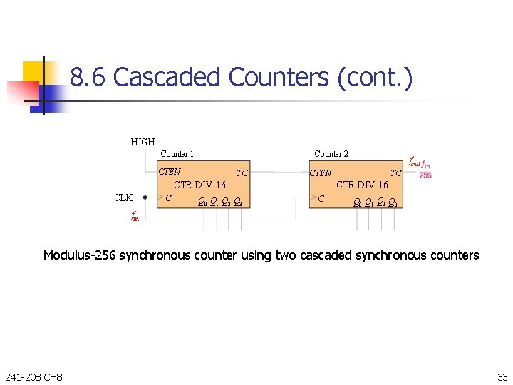
8. 6 Cascaded Counters (cont. ) HIGH Counter 2 Counter 1 CTEN TC CTEN CTR DIV 16 CLK C Q 0 Q 1 Q 2 Q 3 fout TC CTR DIV 16 C Q 0 Q 1 Q 2 Q 3 fin Modulus-256 synchronous counter using two cascaded synchronous counters 241 -208 CH 8 33
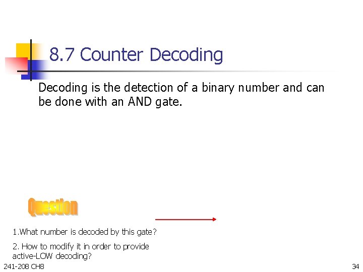
8. 7 Counter Decoding is the detection of a binary number and can be done with an AND gate. 1. What number is decoded by this gate? 2. How to modify it in order to provide active-LOW decoding? 241 -208 CH 8 34
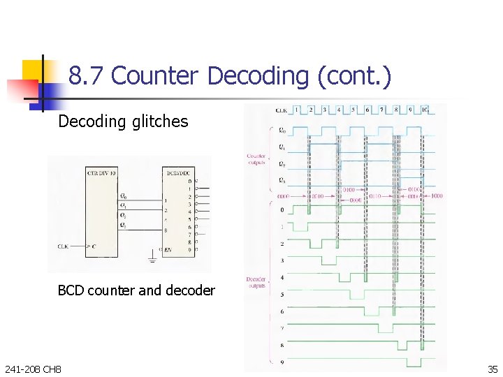
8. 7 Counter Decoding (cont. ) Decoding glitches BCD counter and decoder 241 -208 CH 8 35
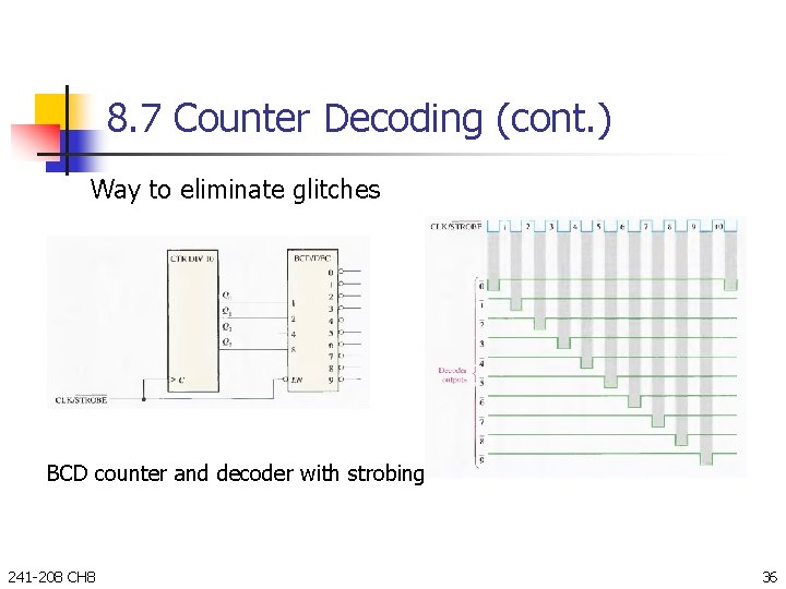
8. 7 Counter Decoding (cont. ) Way to eliminate glitches BCD counter and decoder with strobing 241 -208 CH 8 36
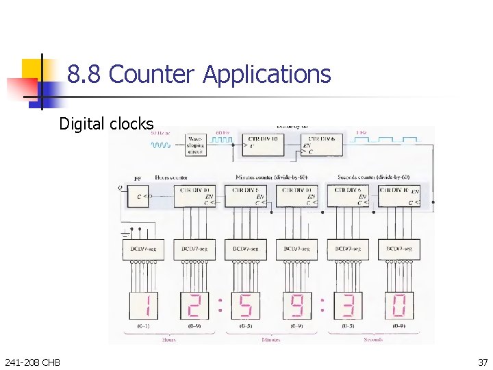
8. 8 Counter Applications Digital clocks 241 -208 CH 8 37
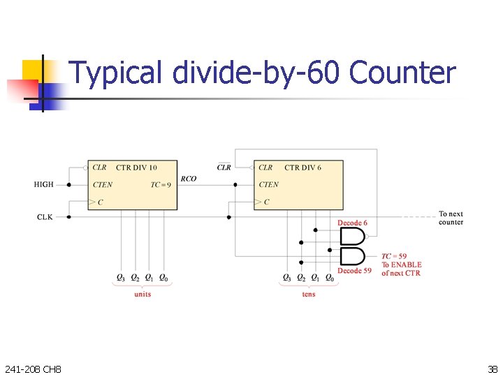
Typical divide-by-60 Counter 241 -208 CH 8 38
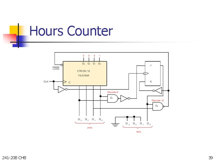
Hours Counter 241 -208 CH 8 39
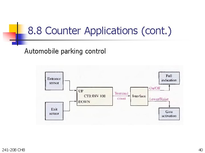
8. 8 Counter Applications (cont. ) Automobile parking control 241 -208 CH 8 40
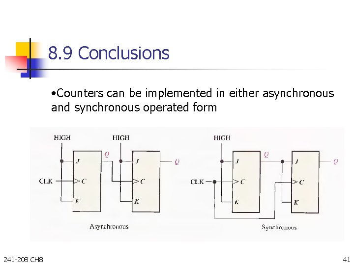
8. 9 Conclusions • Counters can be implemented in either asynchronous and synchronous operated form 241 -208 CH 8 41
- Slides: 41