CHAPTER 8 Combinational Circuit design and Simulation Using
CHAPTER 8 Combinational Circuit design and Simulation Using Gate This chapter in the book includes: Objectives Study Guide 8. 1 Review of Combinational Circuit Design 8. 2 Design of Circuits with Limited Gate Fan-in 8. 3 Gate delays and Timing Diagrams 8. 4 Hazards in Combinational Logic 8. 5 Simulation and Testing of Logic Circuits
Objectives Topics introduced in this chapter: • Draw a timing diagram for a combinational circuit with gate delays. • Define static 0 -and 1 -hazards and dynamic hazard. Given a combinational circuit, find all of the static 0 -and 1 -hazards. For each hazard, specify the order in which the gate outputs must switch in order for the hazard to actually produce a false output. • Given switching function, realize it using a two-level circuit which is free of static and dynamic hazards (for single input variable changes). • Design a multiple-output NAND or NOR circuit using gates with limited fan-in. • Explain the operation of a logic simulator that uses four-valued logic. • Test and debug a logic circuit design using a simulator.
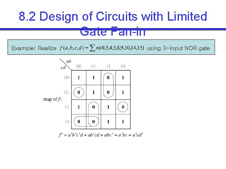
8. 2 Design of Circuits with Limited Gate Fan-in Example: Realize using 3 -input NOR gate
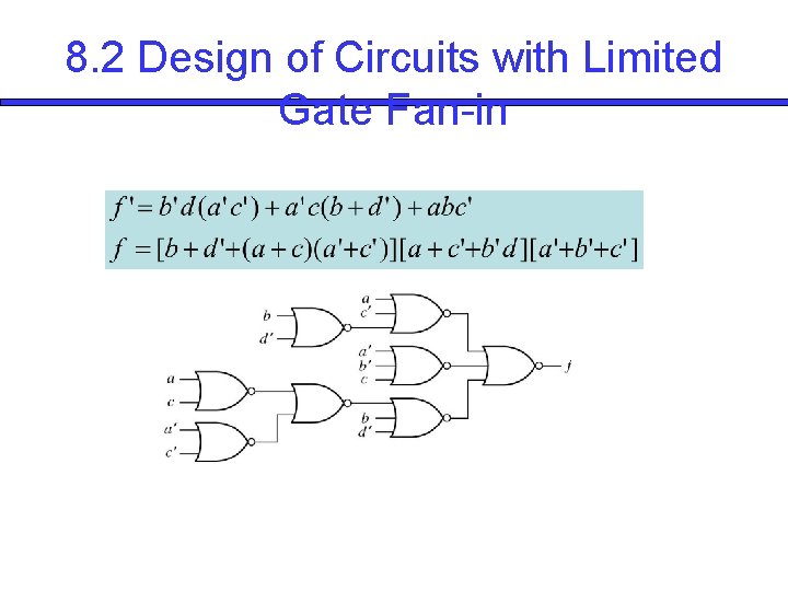
8. 2 Design of Circuits with Limited Gate Fan-in
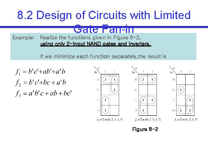
8. 2 Design of Circuits with Limited Gate Fan-in Example: Realize the functions given in Figure 8 -2, using only 2 -input NAND gates and inverters. If we minimize each function separately, the result is Figure 8 -2
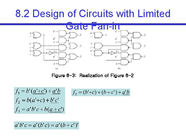
8. 2 Design of Circuits with Limited Gate Fan-in Figure 8 -3: Realization of Figure 8 -2
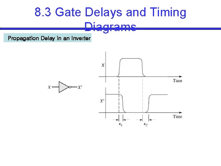
8. 3 Gate Delays and Timing Diagrams Propagation Delay in an Inverter
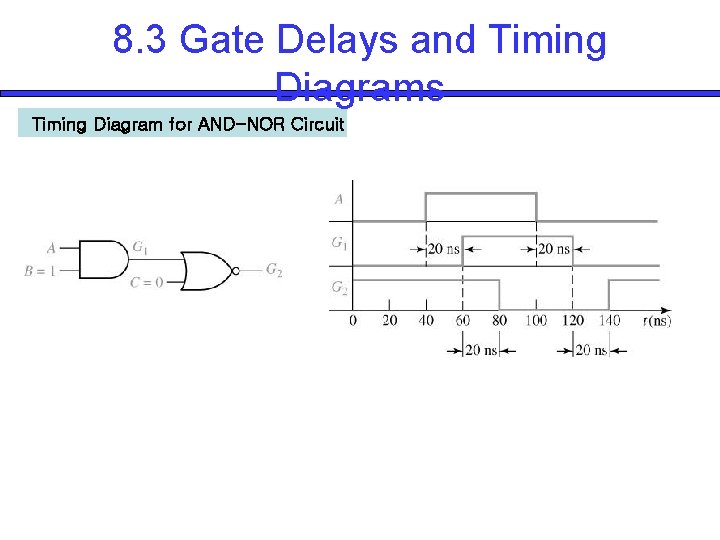
8. 3 Gate Delays and Timing Diagrams Timing Diagram for AND-NOR Circuit
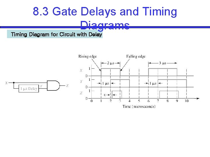
8. 3 Gate Delays and Timing Diagrams Timing Diagram for Circuit with Delay
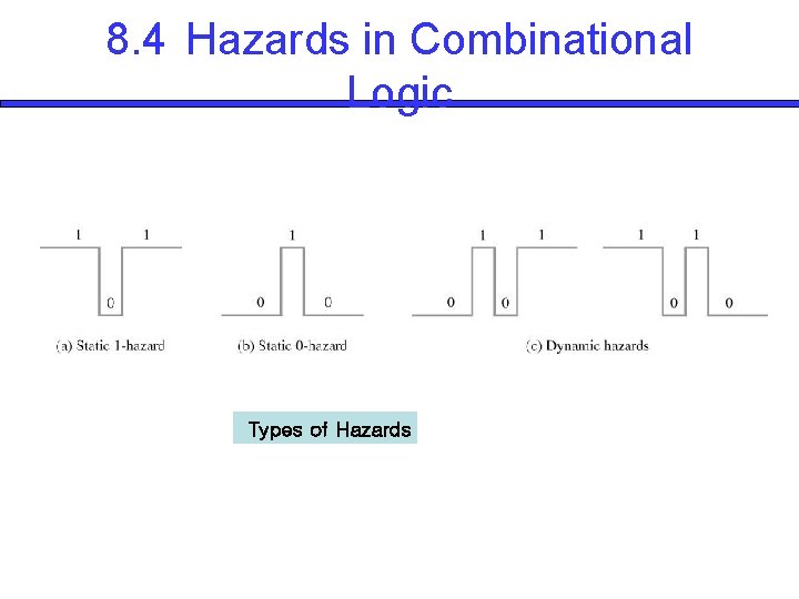
8. 4 Hazards in Combinational Logic Types of Hazards
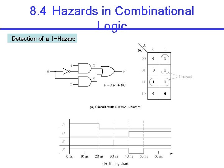
8. 4 Hazards in Combinational Logic Detection of a 1 -Hazard
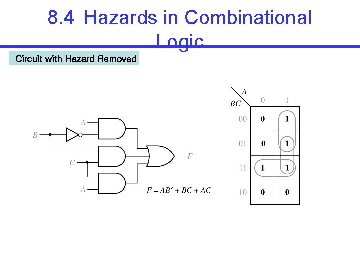
8. 4 Hazards in Combinational Logic Circuit with Hazard Removed
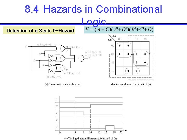
8. 4 Hazards in Combinational Logic Detection of a Static 0 -Hazard
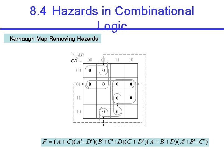
8. 4 Hazards in Combinational Logic Karnaugh Map Removing Hazards
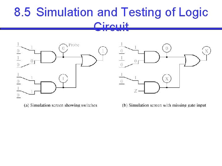
8. 5 Simulation and Testing of Logic Circuit
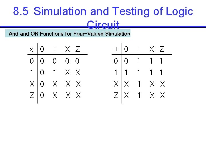
8. 5 Simulation and Testing of Logic Circuit And and OR Functions for Four-Valued Simulation x 0 1 X Z 0 0 0 1 X X X 0 X X X Z 0 X X X + 0 1 X Z 0 0 1 X X 1 1 1 X X Z 1 1 X X
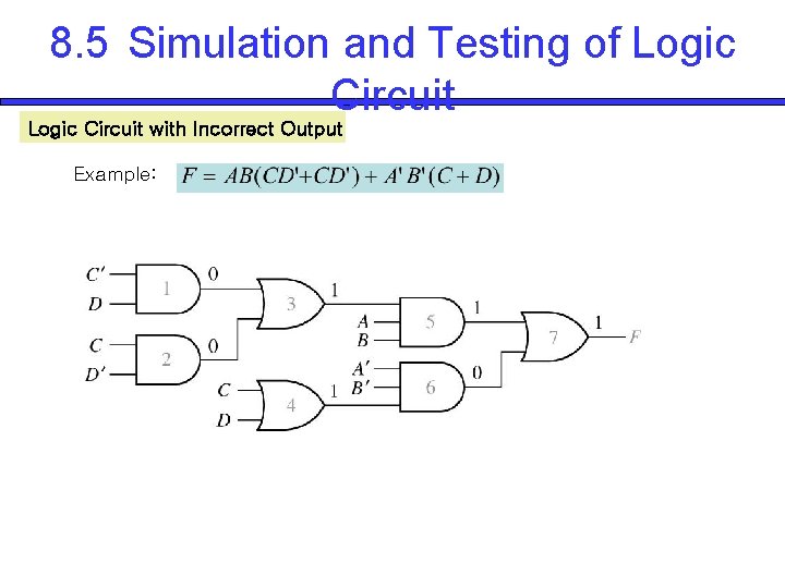
8. 5 Simulation and Testing of Logic Circuit with Incorrect Output Example:
- Slides: 17