Chapter 7 Parallel port General Purpose Input Output


- Slides: 50

Chapter 7: Parallel port (General Purpose Input Output, GPIO) --Driving Parallel Loads CEG 2400 - Microcomputer Systems CENG 2400 Ch 7: driving parallel loads v. 7 a 1

Practical digital circuit interfacing Kh wong CENG 2400 Ch 7: driving parallel loads v. 7 a 2

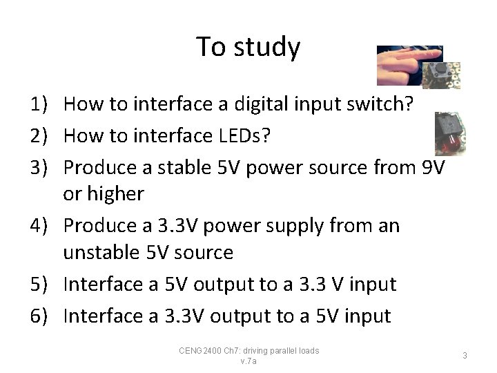
To study 1) How to interface a digital input switch? 2) How to interface LEDs? 3) Produce a stable 5 V power source from 9 V or higher 4) Produce a 3. 3 V power supply from an unstable 5 V source 5) Interface a 5 V output to a 3. 3 V input 6) Interface a 3. 3 V output to a 5 V input CENG 2400 Ch 7: driving parallel loads v. 7 a 3

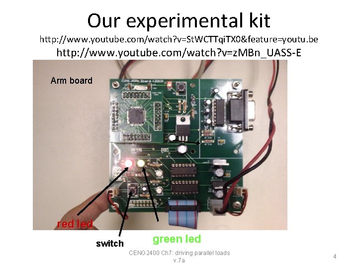
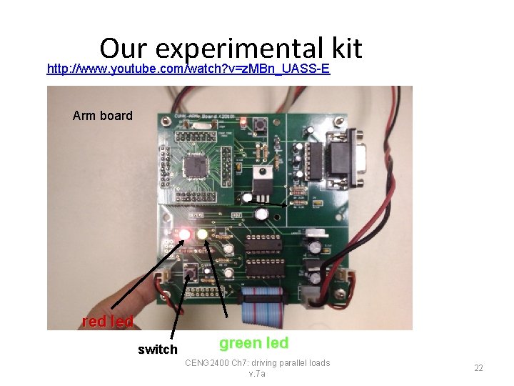
Our experimental kit http: //www. youtube. com/watch? v=St. WCTTqi. TX 0&feature=youtu. be http: //www. youtube. com/watch? v=z. MBn_UASS-E Arm board red led switch green led CENG 2400 Ch 7: driving parallel loads v. 7 a 4

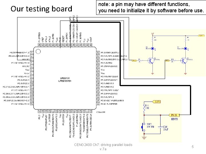
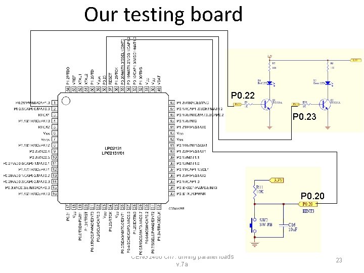
Our testing board note: a pin may have different functions, you need to initialize it by software before use. • CENG 2400 Ch 7: driving parallel loads v. 7 a 5

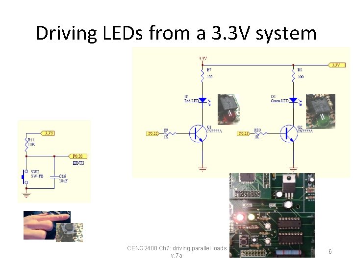
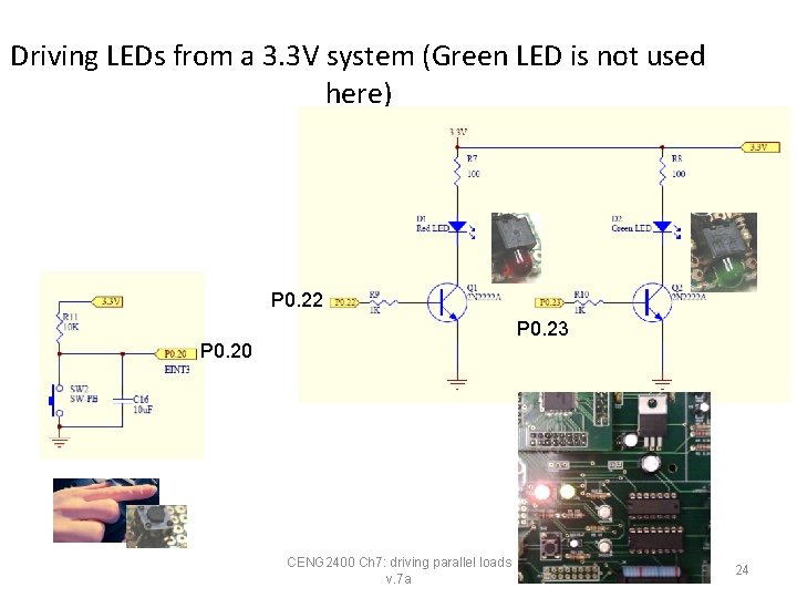
Driving LEDs from a 3. 3 V system CENG 2400 Ch 7: driving parallel loads v. 7 a 6

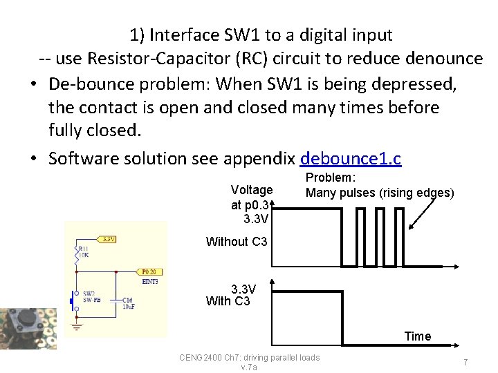
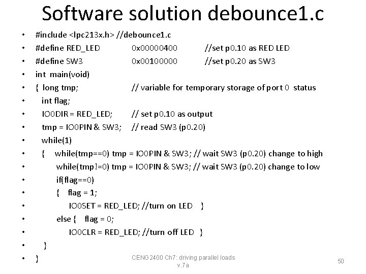
1) Interface SW 1 to a digital input -- use Resistor-Capacitor (RC) circuit to reduce denounce • De-bounce problem: When SW 1 is being depressed, the contact is open and closed many times before fully closed. • Software solution see appendix debounce 1. c Voltage at p 0. 3 3. 3 V Problem: Many pulses (rising edges) Without C 3 3. 3 V With C 3 Time CENG 2400 Ch 7: driving parallel loads v. 7 a 7

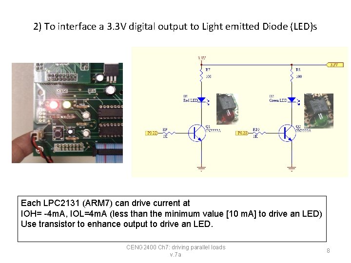
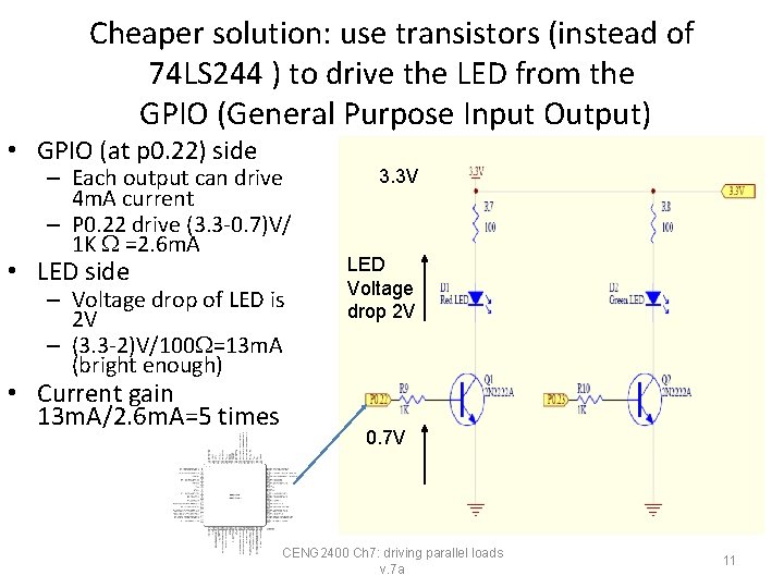
2) To interface a 3. 3 V digital output to Light emitted Diode (LED)s Each LPC 2131 (ARM 7) can drive current at IOH= -4 m. A, IOL=4 m. A (less than the minimum value [10 m. A] to drive an LED) Use transistor to enhance output to drive an LED. CENG 2400 Ch 7: driving parallel loads v. 7 a 8

Warning • You cannot drive directly an LED from a GPIO (General Purpose Input Output) pin of a LPC 2131(ARM 7) microcontroller • The current required by the LED (>10 m. A) may cause damage to the GPIO circuitry inside the LPC 2131(ARM 7) microcontroller • Solution: use transistors or 74 LS 244 line buffers to amplifier the current to drive the LEDs CENG 2400 Ch 7: driving parallel loads v. 7 a 9

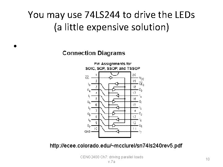
You may use 74 LS 244 to drive the LEDs (a little expensive solution) • http: //ecee. colorado. edu/~mcclurel/sn 74 ls 240 rev 5. pdf CENG 2400 Ch 7: driving parallel loads v. 7 a 10

Cheaper solution: use transistors (instead of 74 LS 244 ) to drive the LED from the GPIO (General Purpose Input Output) • GPIO (at p 0. 22) side – Each output can drive 4 m. A current – P 0. 22 drive (3. 3 -0. 7)V/ 1 K =2. 6 m. A • LED side – Voltage drop of LED is 2 V – (3. 3 -2)V/100 =13 m. A (bright enough) • Current gain 13 m. A/2. 6 m. A=5 times 3. 3 V LED Voltage drop 2 V 0. 7 V CENG 2400 Ch 7: driving parallel loads v. 7 a 11

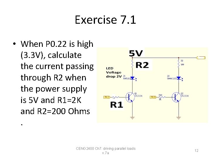
Exercise 7. 1 • When P 0. 22 is high (3. 3 V), calculate the current passing through R 2 when the power supply is 5 V and R 1=2 K and R 2=200 Ohms. CENG 2400 Ch 7: driving parallel loads v. 7 a 12

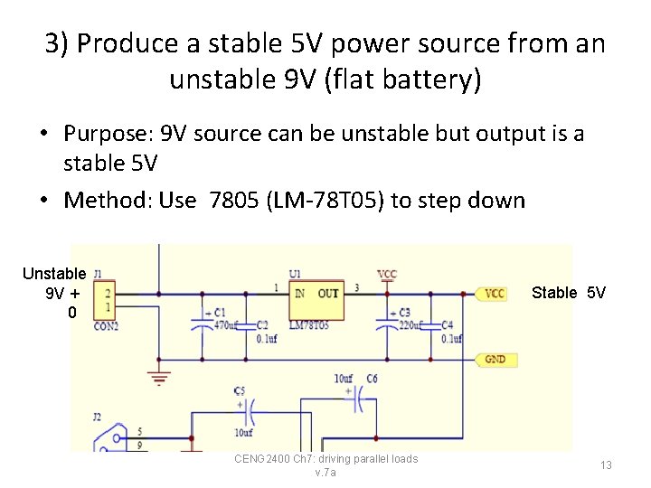
3) Produce a stable 5 V power source from an unstable 9 V (flat battery) • Purpose: 9 V source can be unstable but output is a stable 5 V • Method: Use 7805 (LM-78 T 05) to step down Unstable 9 V + 0 Stable 5 V CENG 2400 Ch 7: driving parallel loads v. 7 a 13

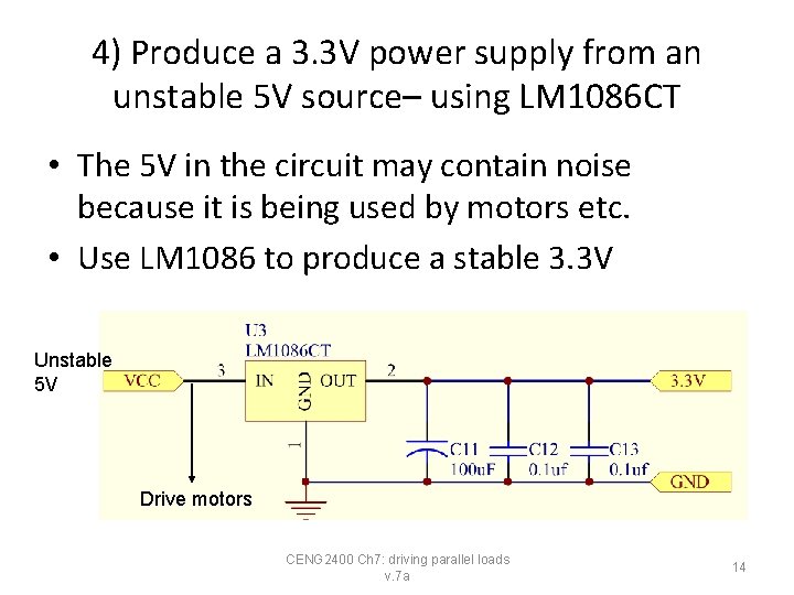
4) Produce a 3. 3 V power supply from an unstable 5 V source– using LM 1086 CT • The 5 V in the circuit may contain noise because it is being used by motors etc. • Use LM 1086 to produce a stable 3. 3 V Unstable 5 V Drive motors CENG 2400 Ch 7: driving parallel loads v. 7 a 14

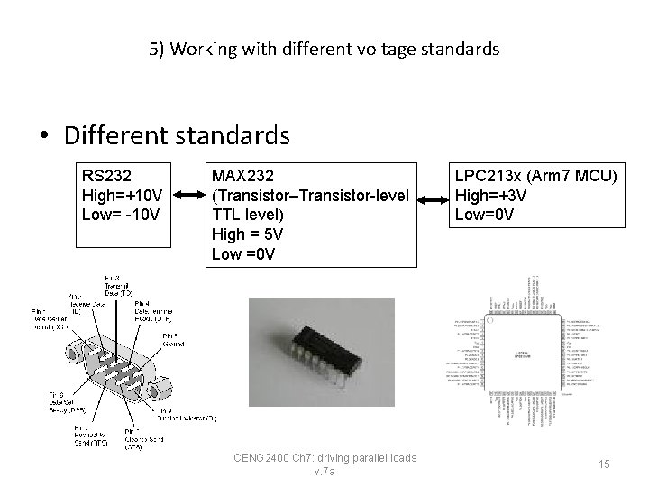
5) Working with different voltage standards • Different standards RS 232 High=+10 V Low= -10 V MAX 232 (Transistor–Transistor-level TTL level) High = 5 V Low =0 V CENG 2400 Ch 7: driving parallel loads v. 7 a LPC 213 x (Arm 7 MCU) High=+3 V Low=0 V 15

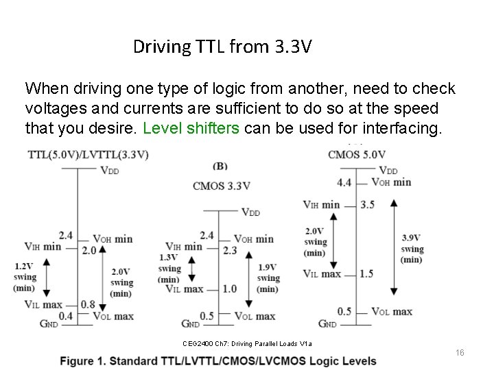
Driving TTL from 3. 3 V When driving one type of logic from another, need to check voltages and currents are sufficient to do so at the speed that you desire. Level shifters can be used for interfacing. CEG 2400 Ch 7: Driving Parallel Loads V 1 a CENG 2400 Ch 7: driving parallel loads v. 7 a 16

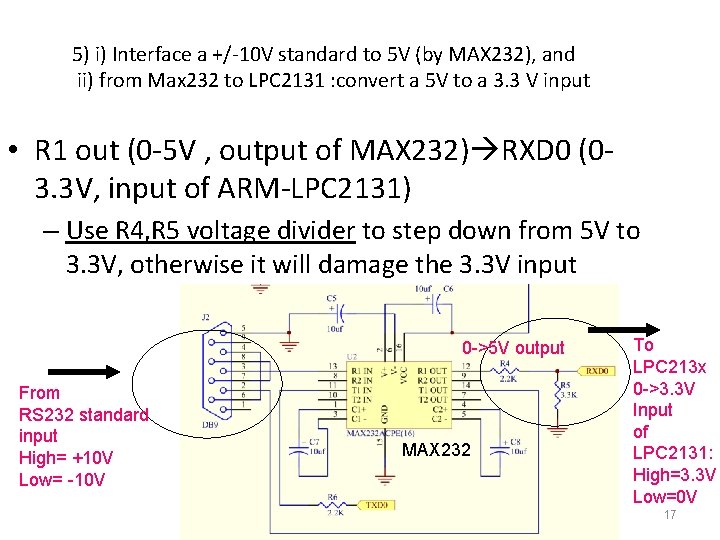
5) i) Interface a +/-10 V standard to 5 V (by MAX 232), and ii) from Max 232 to LPC 2131 : convert a 5 V to a 3. 3 V input • R 1 out (0 -5 V , output of MAX 232) RXD 0 (03. 3 V, input of ARM-LPC 2131) – Use R 4, R 5 voltage divider to step down from 5 V to 3. 3 V, otherwise it will damage the 3. 3 V input 0 ->5 V output From RS 232 standard input High= +10 V Low= -10 V MAX 232 CENG 2400 Ch 7: driving parallel loads v. 7 a To LPC 213 x 0 ->3. 3 V Input of LPC 2131: High=3. 3 V Low=0 V 17

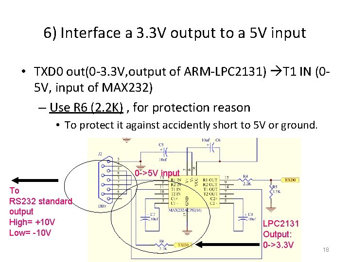
6) Interface a 3. 3 V output to a 5 V input • TXD 0 out(0 -3. 3 V, output of ARM-LPC 2131) T 1 IN (05 V, input of MAX 232) – Use R 6 (2. 2 K) , for protection reason • To protect it against accidently short to 5 V or ground. 0 ->5 V input To RS 232 standard output High= +10 V Low= -10 V CENG 2400 Ch 7: driving parallel loads v. 7 a LPC 2131 Output: 0 ->3. 3 V 18

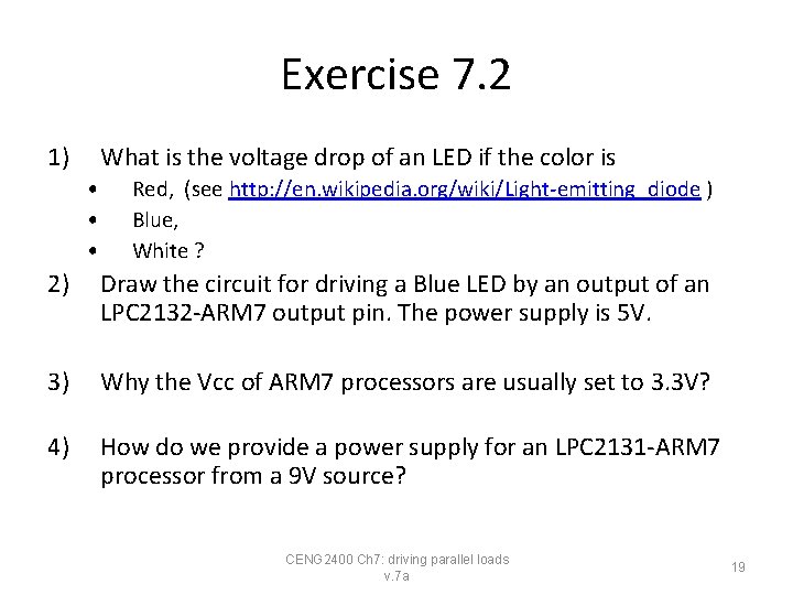
Exercise 7. 2 1) What is the voltage drop of an LED if the color is • • • Red, (see http: //en. wikipedia. org/wiki/Light-emitting_diode ) Blue, White ? 2) Draw the circuit for driving a Blue LED by an output of an LPC 2132 -ARM 7 output pin. The power supply is 5 V. 3) Why the Vcc of ARM 7 processors are usually set to 3. 3 V? 4) How do we provide a power supply for an LPC 2131 -ARM 7 processor from a 9 V source? CENG 2400 Ch 7: driving parallel loads v. 7 a 19

Part 2 Use of LPC 2131(ARM 7) –GPIO (General Purpose Input Output) to drive an LED and read a switch CENG 2400 Ch 7: driving parallel loads v. 7 a 20

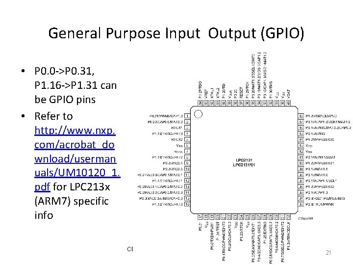
General Purpose Input Output (GPIO) • P 0. 0 ->P 0. 31, P 1. 16 ->P 1. 31 can be GPIO pins • Refer to http: //www. nxp. com/acrobat_do wnload/userman uals/UM 10120_1. pdf for LPC 213 x (ARM 7) specific info CENG 2400 Ch 7: driving parallel loads v. 7 a 21 21

Our experimental kit http: //www. youtube. com/watch? v=z. MBn_UASS-E Arm board red led switch green led CENG 2400 Ch 7: driving parallel loads v. 7 a 22

Our testing board • P 0. 22 P 0. 23 P 0. 20 CENG 2400 Ch 7: driving parallel loads v. 7 a 23

Driving LEDs from a 3. 3 V system (Green LED is not used here) P 0. 22 P 0. 23 P 0. 20 CENG 2400 Ch 7: driving parallel loads v. 7 a 24

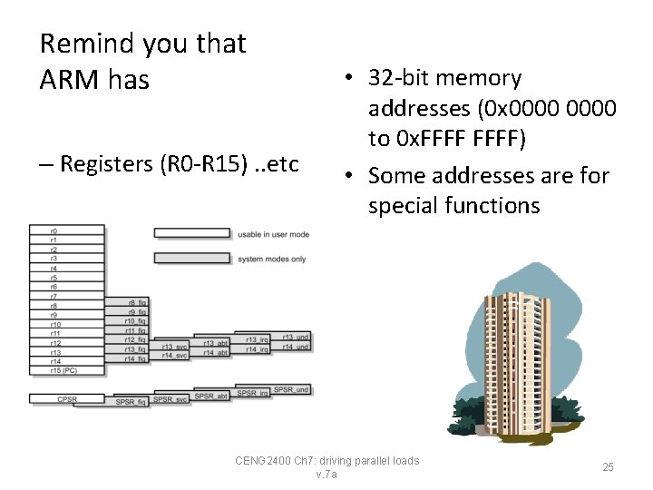
Remind you that ARM has – Registers (R 0 -R 15). . etc • 32 -bit memory addresses (0 x 0000 to 0 x. FFFF) • Some addresses are for special functions CENG 2400 Ch 7: driving parallel loads v. 7 a 25

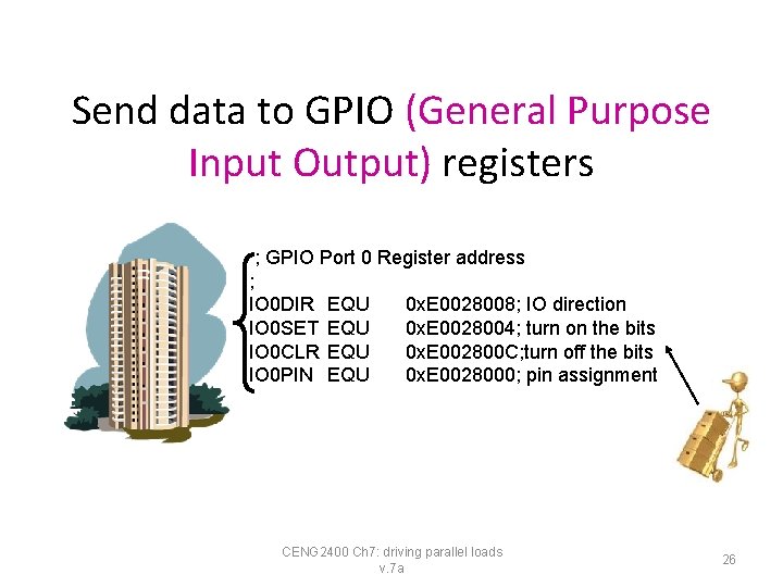
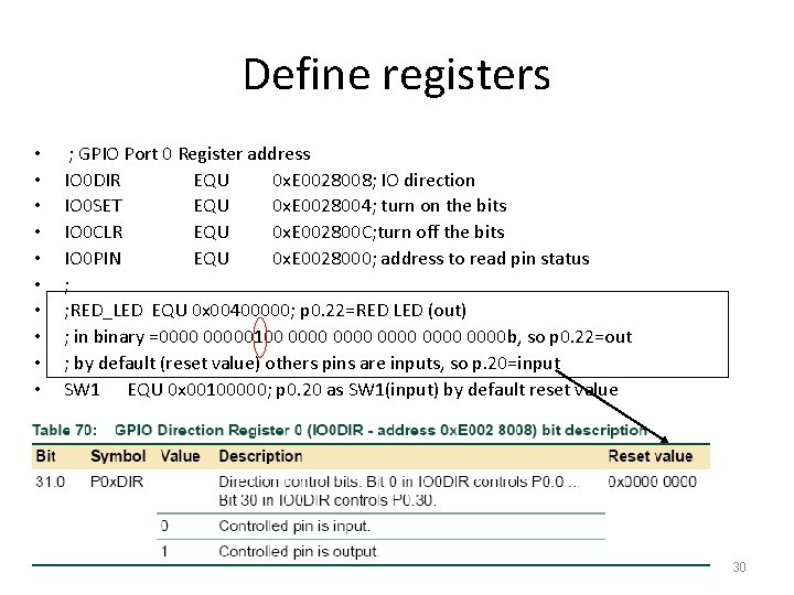
Send data to GPIO (General Purpose Input Output) registers ; GPIO Port 0 Register address ; IO 0 DIR IO 0 SET IO 0 CLR IO 0 PIN EQU EQU 0 x. E 0028008; IO direction 0 x. E 0028004; turn on the bits 0 x. E 002800 C; turn off the bits 0 x. E 0028000; pin assignment CENG 2400 Ch 7: driving parallel loads v. 7 a 26

The experiment software in (i) Assembly or (ii) C CENG 2400 Ch 7: driving parallel loads v. 7 a 27

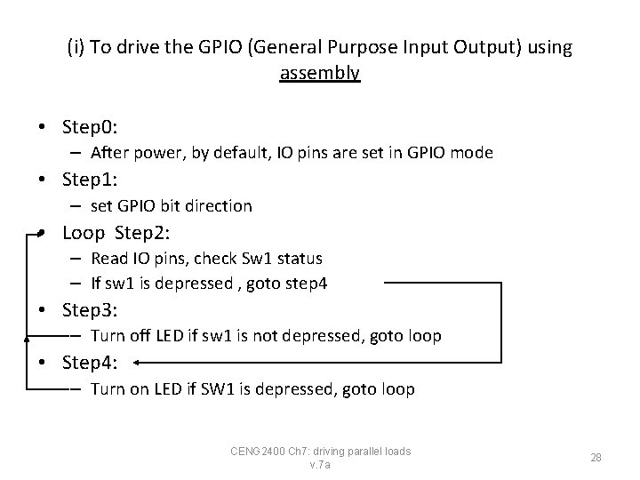
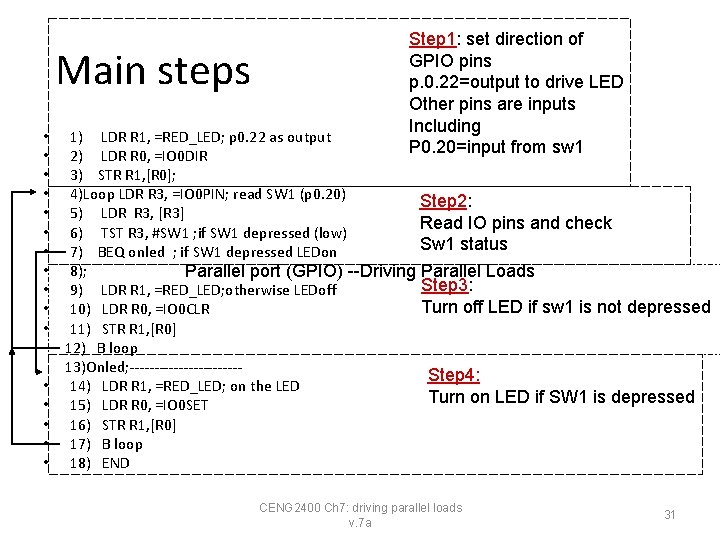
(i) To drive the GPIO (General Purpose Input Output) using assembly • Step 0: – After power, by default, IO pins are set in GPIO mode • Step 1: – set GPIO bit direction • Loop Step 2: – Read IO pins, check Sw 1 status – If sw 1 is depressed , goto step 4 • Step 3: – Turn off LED if sw 1 is not depressed, goto loop • Step 4: – Turn on LED if SW 1 is depressed, goto loop CENG 2400 Ch 7: driving parallel loads v. 7 a 28

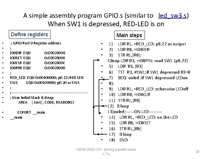
A simple assembly program GPIO. s (similar to led_sw 3. s) When SW 1 is depressed, RED-LED is on Define registers Main steps • • • • ; GPIO Port 0 Register address ; IO 0 DIR EQU 0 x. E 0028008 IO 0 SET EQU 0 x. E 0028004 IO 0 CLR EQU 0 x. E 002800 C IO 0 PIN EQU 0 x. E 0028000 ; RED_LED EQU 0 x 00400000; p 0. 22=RED LED SW 1 EQU 0 x 00100000; p 0. 20 as SW 1 ; ; ------------------------------; User Initial Stack & Heap AREA |. text|, CODE, READONLY • • EXPORT __main • • • • 1) LDR R 1, =RED_LED; p 0. 22 as output 2) LDR R 0, =IO 0 DIR 3) STR R 1, [R 0]; 4)loop LDR R 3, =IO 0 PIN; read SW 1 (p 0. 22) 5) LDR R 3, [R 3] 6) TST R 3, #SW 1; if SW 1 depressed R 3=0 7) BEQ onled ; if SW 1 depressed LEDon 8); 9) LDR R 1, =RED_LED ; otherwise LEDoff 10) LDR R 0, =IO 0 CLR 11) STR R 1, [R 0] 12) B loop 13)onled; ------ON LED----14) LDR R 1, =RED_LED; on the LED 15) LDR R 0, =IO 0 SET 16) STR R 1, [R 0] 17) B loop 18) END CENG 2400 Ch 7: driving parallel loads v. 7 a 29

Define registers • • • ; GPIO Port 0 Register address IO 0 DIR EQU 0 x. E 0028008; IO direction IO 0 SET EQU 0 x. E 0028004; turn on the bits IO 0 CLR EQU 0 x. E 002800 C; turn off the bits IO 0 PIN EQU 0 x. E 0028000; address to read pin status ; ; RED_LED EQU 0 x 00400000; p 0. 22=RED LED (out) ; in binary =00000100 0000 0000 b, so p 0. 22=out ; by default (reset value) others pins are inputs, so p. 20=input SW 1 EQU 0 x 00100000; p 0. 20 as SW 1(input) by default reset value CENG 2400 Ch 7: driving parallel loads v. 7 a 30

Main steps • • • • Step 1: set direction of GPIO pins p. 0. 22=output to drive LED Other pins are inputs Including P 0. 20=input from sw 1 1) LDR R 1, =RED_LED; p 0. 22 as output 2) LDR R 0, =IO 0 DIR 3) STR R 1, [R 0]; 4)Loop LDR R 3, =IO 0 PIN; read SW 1 (p 0. 20) Step 2: 5) LDR R 3, [R 3] Read IO pins and check 6) TST R 3, #SW 1 ; if SW 1 depressed (low) Sw 1 status 7) BEQ onled ; if SW 1 depressed LEDon 8); Parallel port (GPIO) --Driving Parallel Loads Step 3: 9) LDR R 1, =RED_LED; otherwise LEDoff Turn off LED if sw 1 is not depressed 10) LDR R 0, =IO 0 CLR 11) STR R 1, [R 0] 12) B loop 13)Onled; -----------Step 4: 14) LDR R 1, =RED_LED; on the LED Turn on LED if SW 1 is depressed 15) LDR R 0, =IO 0 SET 16) STR R 1, [R 0] 17) B loop 18) END CENG 2400 Ch 7: driving parallel loads v. 7 a 31

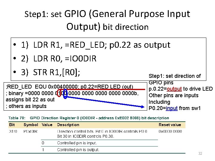
Step 1: set GPIO (General Purpose Input Output) bit direction • 1) LDR R 1, =RED_LED; p 0. 22 as output • 2) LDR R 0, =IO 0 DIR • 3) STR R 1, [R 0]; Step 1: set direction of ; RED_LED EQU 0 x 00400000; p 0. 22=RED LED (out) ; binary =0000 0100 0000 0000 b, assigns bit 22 as out ; others as inputs CENG 2400 Ch 7: driving parallel loads v. 7 a GPIO pins p. 0. 22=output to drive LED Other pins are inputs Including P 0. 20=input from sw 1 32

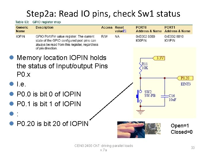
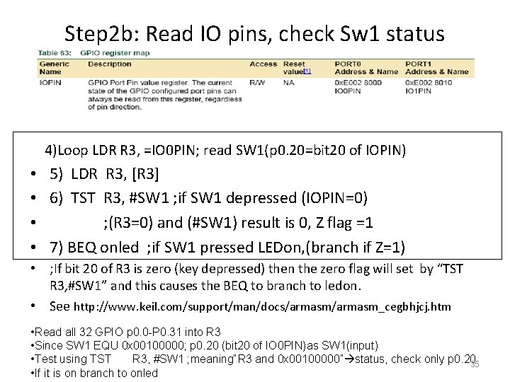
Step 2 a: Read IO pins, check Sw 1 status • l Memory location IOPIN holds the status of Input/output Pins P 0. x l I. e. l P 0. 0 is bit 0 of IOPIN l P 0. 1 is bit 1 of IOPIN l: l P 0. 20 is bit 20 of IOPIN CENG 2400 Ch 7: driving parallel loads v. 7 a Open=1 Closed=0 33

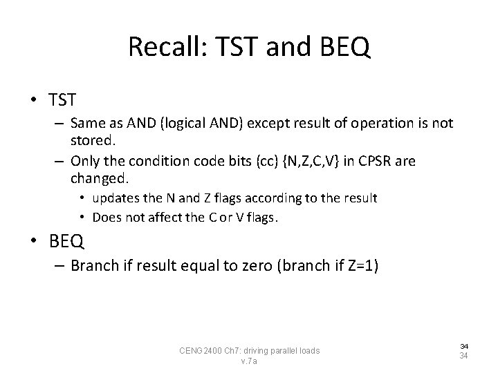
Recall: TST and BEQ • TST – Same as AND (logical AND) except result of operation is not stored. – Only the condition code bits (cc) {N, Z, C, V} in CPSR are changed. • updates the N and Z flags according to the result • Does not affect the C or V flags. • BEQ – Branch if result equal to zero (branch if Z=1) CENG 2400 Ch 7: driving parallel loads v. 7 a 34 34

Step 2 b: Read IO pins, check Sw 1 status 4)Loop LDR R 3, =IO 0 PIN; read SW 1(p 0. 20=bit 20 of IOPIN) • 5) LDR R 3, [R 3] • 6) TST R 3, #SW 1 ; if SW 1 depressed (IOPIN=0) • ; (R 3=0) and (#SW 1) result is 0, Z flag =1 • 7) BEQ onled ; if SW 1 pressed LEDon, (branch if Z=1) • ; If bit 20 of R 3 is zero (key depressed) then the zero flag will set by “TST R 3, #SW 1” and this causes the BEQ to branch to ledon. • See http: //www. keil. com/support/man/docs/armasm_cegbhjcj. htm • Read all 32 GPIO p 0. 0 -P 0. 31 into R 3 • Since SW 1 EQU 0 x 00100000; p 0. 20 (bit 20 of IO 0 PIN)as SW 1(input) 35 Ch 7: driving loads • Test using TST R 3, #SW 1 CENG 2400 ; meaning“R 3 and parallel 0 x 00100000” status, check only p 0. 20 35 v. 7 a • If it is on branch to onled

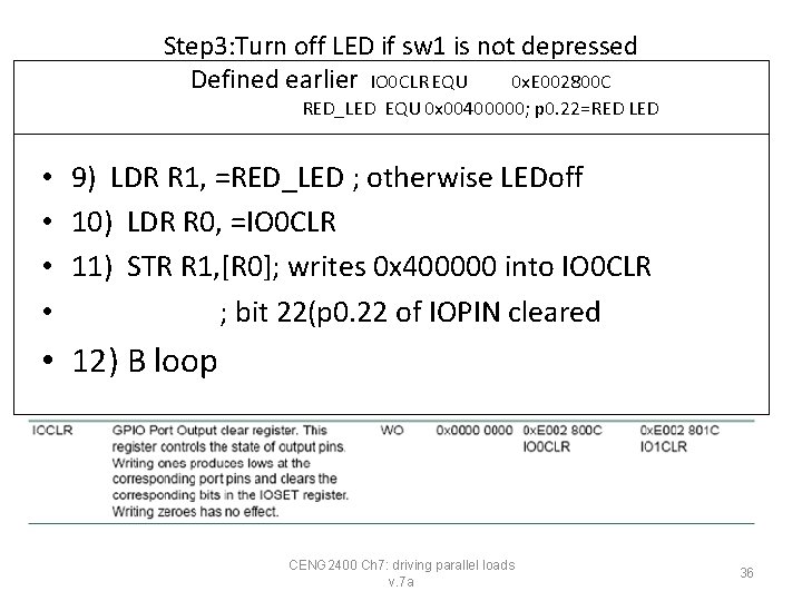
Step 3: Turn off LED if sw 1 is not depressed Defined earlier IO 0 CLR EQU 0 x. E 002800 C RED_LED EQU 0 x 00400000; p 0. 22=RED LED • 9) LDR R 1, =RED_LED ; otherwise LEDoff • 10) LDR R 0, =IO 0 CLR • 11) STR R 1, [R 0]; writes 0 x 400000 into IO 0 CLR • ; bit 22(p 0. 22 of IOPIN cleared • 12) B loop CENG 2400 Ch 7: driving parallel loads v. 7 a 36

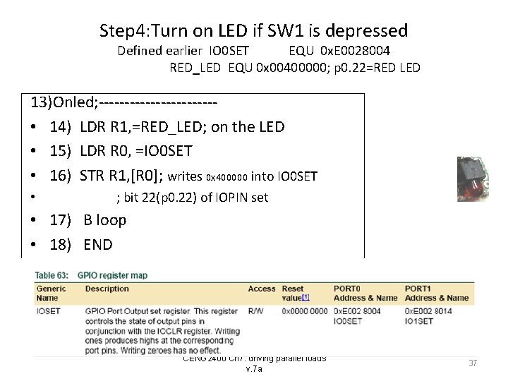
Step 4: Turn on LED if SW 1 is depressed Defined earlier IO 0 SET EQU 0 x. E 0028004 RED_LED EQU 0 x 00400000; p 0. 22=RED LED 13)Onled; ----------- • 14) LDR R 1, =RED_LED; on the LED • 15) LDR R 0, =IO 0 SET • 16) STR R 1, [R 0]; writes 0 x 400000 into IO 0 SET • ; bit 22(p 0. 22) of IOPIN set • 17) B loop • 18) END CENG 2400 Ch 7: driving parallel loads v. 7 a 37 37

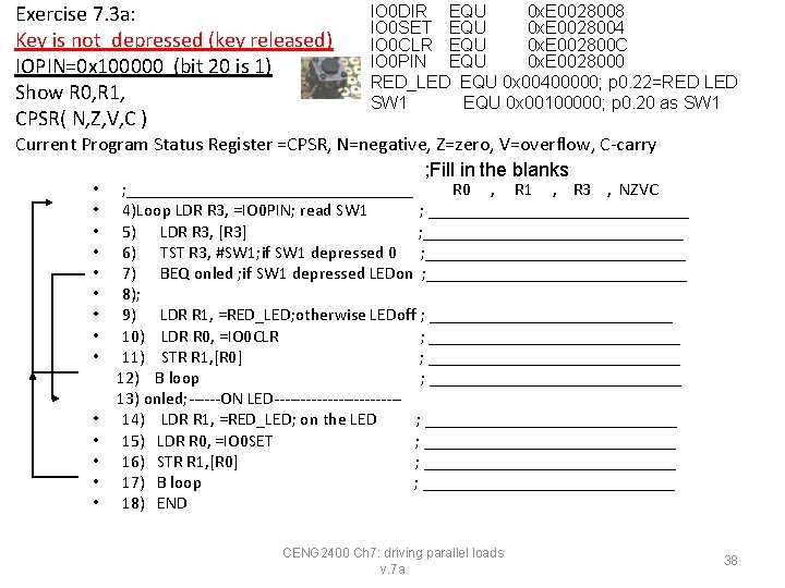
Exercise 7. 3 a: Key is not_depressed (key released) IOPIN=0 x 100000 (bit 20 is 1) Show R 0, R 1, CPSR( N, Z, V, C ) IO 0 DIR EQU 0 x. E 0028008 IO 0 SET EQU 0 x. E 0028004 IO 0 CLR EQU 0 x. E 002800 C IO 0 PIN EQU 0 x. E 0028000 RED_LED EQU 0 x 00400000; p 0. 22=RED LED SW 1 EQU 0 x 00100000; p 0. 20 as SW 1 Current Program Status Register =CPSR, N=negative, Z=zero, V=overflow, C-carry ; Fill in the blanks • • • • ; _________________ R 0 , R 1 , R 3 , NZVC 4)Loop LDR R 3, =IO 0 PIN; read SW 1 ; _______________ 5) LDR R 3, [R 3] ; _______________ 6) TST R 3, #SW 1; if SW 1 depressed 0 ; _______________ 7) BEQ onled ; if SW 1 depressed LEDon ; _______________ 8); 9) LDR R 1, =RED_LED; otherwise LEDoff ; ______________ 10) LDR R 0, =IO 0 CLR ; _______________ 11) STR R 1, [R 0] ; _______________ 12) B loop ; _______________ 13) onled; ------ON LED------------14) LDR R 1, =RED_LED; on the LED ; _______________ 15) LDR R 0, =IO 0 SET ; _______________ 16) STR R 1, [R 0] ; _______________ 17) B loop ; _______________ 18) END CENG 2400 Ch 7: driving parallel loads v. 7 a 38

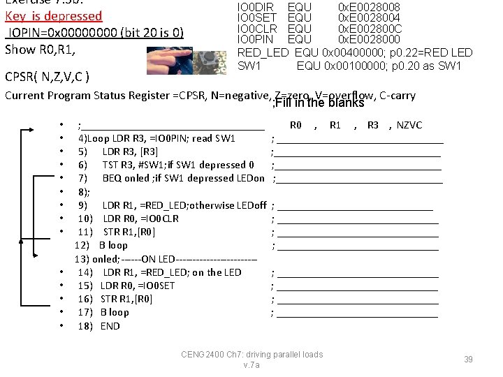
Exercise 7. 3 b: Key is depressed IOPIN=0 x 0000 (bit 20 is 0) Show R 0, R 1, CPSR( N, Z, V, C ) IO 0 DIR EQU 0 x. E 0028008 IO 0 SET EQU 0 x. E 0028004 IO 0 CLR EQU 0 x. E 002800 C IO 0 PIN EQU 0 x. E 0028000 RED_LED EQU 0 x 00400000; p 0. 22=RED LED SW 1 EQU 0 x 00100000; p 0. 20 as SW 1 Current Program Status Register =CPSR, N=negative, Z=zero, V=overflow, C-carry ; Fill in the blanks • • • • ; _________________ 4)Loop LDR R 3, =IO 0 PIN; read SW 1 5) LDR R 3, [R 3] 6) TST R 3, #SW 1; if SW 1 depressed 0 7) BEQ onled ; if SW 1 depressed LEDon 8); 9) LDR R 1, =RED_LED; otherwise LEDoff 10) LDR R 0, =IO 0 CLR 11) STR R 1, [R 0] 12) B loop 13) onled; ------ON LED------------14) LDR R 1, =RED_LED; on the LED 15) LDR R 0, =IO 0 SET 16) STR R 1, [R 0] 17) B loop 18) END R 0 , R 1 , R 3 , NZVC ; ______________________________ ; _____________________________ ; _____________________________ CENG 2400 Ch 7: driving parallel loads v. 7 a 39

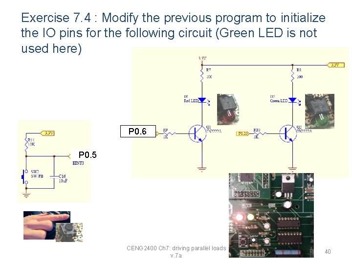
Exercise 7. 4 : Modify the previous program to initialize the IO pins for the following circuit (Green LED is not used here) P 0. 6 P 0. 5 CENG 2400 Ch 7: driving parallel loads v. 7 a 40

(i) To drive the GPIO (General Purpose Input Output) Using C A much simpler solution CENG 2400 Ch 7: driving parallel loads v. 7 a 41 41

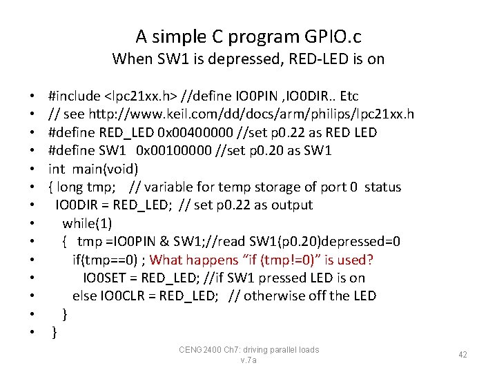
A simple C program GPIO. c When SW 1 is depressed, RED-LED is on • • • • #include <lpc 21 xx. h> //define IO 0 PIN , IO 0 DIR. . Etc // see http: //www. keil. com/dd/docs/arm/philips/lpc 21 xx. h #define RED_LED 0 x 00400000 //set p 0. 22 as RED LED #define SW 1 0 x 00100000 //set p 0. 20 as SW 1 int main(void) { long tmp; // variable for temp storage of port 0 status IO 0 DIR = RED_LED; // set p 0. 22 as output while(1) { tmp =IO 0 PIN & SW 1; //read SW 1(p 0. 20)depressed=0 if(tmp==0) ; What happens “if (tmp!=0)” is used? IO 0 SET = RED_LED; //if SW 1 pressed LED is on else IO 0 CLR = RED_LED; // otherwise off the LED } } CENG 2400 Ch 7: driving parallel loads v. 7 a 42

Summary • Learned how to interface parallel GPIO (General Purpose Input Output) loads • Learned how to drive LEDs using the ARM MCU CENG 2400 Ch 7: driving parallel loads v. 7 a 43

Appendix CENG 2400 Ch 7: driving parallel loads v. 7 a 44

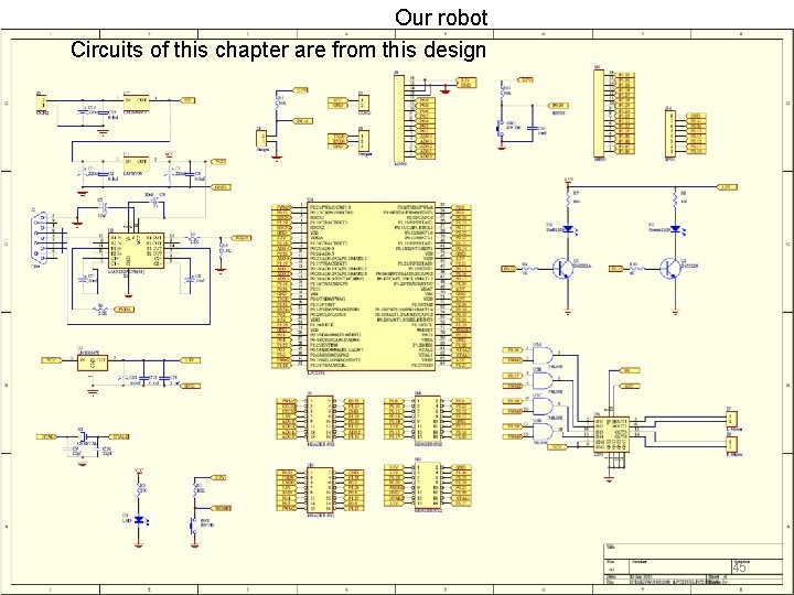
Our robot Circuits of this chapter are from this design CENG 2400 Ch 7: driving parallel loads v. 7 a 45

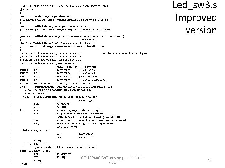
• • • • • • • • • • • • ; led_sw 3. s : Testing GPIO_0 for input/output to be run on the LPC 2131 board ; (ver. 2013) ; ; Exercise 1 : run this program, you should see: ; When you press the button (sw 3), the LED(D 1) is on, otherwise LED(D 1) is off. ; ; Exercise 2: Modified the program so your output is reversed: ; When you press the button (sw 3), the LED(D 1) is off, otherwise LED(D 1) is on. ; ; Exercise 3: Modified the program, so you can use sw 4 (P 0. 11) to control LED D 2 (P 0. 21) ; as in exercise 1. ; Exercise 4: Modified the program, so when you press sw 3 once , ; the LED(D 1) will toggle (change state from on_to_off or off_to_on) ; ; Note: LED(D 1) is at GPIO P 0. 10, sw 3 is at GPIO P 0. 20 (also for EINT 3 external interrupt input) ; Note: LED(D 2) is at GPIO P 0. 11, sw 4 is at GPIO P 0. 21 ; Note: LED(D 3) is at GPIO P 0. 12, sw 5 is at GPIO P 0. 22 ; Note: LED(D 4) is at GPIO P 0. 13, sw 6 is at GPIO P 0. 23 AREA |. data|, DATA, READWRITE IO 0 DIR EQU 0 x. E 0028008 ; pin direction IO 0 SET EQU 0 x. E 0028004 ; pin value set IO 0 CLR EQU 0 x. E 002800 C ; pin value clear IO 0 PIN EQU 0 x. E 0028000 ; pin value read & write RED_LED EQU 0 x 00000400; 0100, 0000 B p 0. 10=RED LED SW 3 EQU 0 x 00100000; 0001, 0000, 0000 B, p 0. 20 is SW 3 AREA |. text|, CODE, READONLY; User Initial Stack & Heap EXPORT __main ; set p 0. 22(red led) as output using the IO 0 DIR register LDR R 1, =RED_LED LDR R 0, =IO 0 DIR STR R 1, [R 0]; loop LDR R 3, =IO 0 PIN; target at the IO 0 PIN register LDR R 3, [R 3]; load IO 0 PIN value to R 3 register ; if the switch is depressed, corresponding pin value is 0 TST R 3, #SW 3; test on pin 20 of IO 0 PIN to see if SW 3 is depressed BEQ onled ; if IO 0 PIN[20]=0, go to onled to light the led ; otherwise LEDoff offled LDR R 1, =RED_LED LDR R 0, =IO 0 CLR STR R 1, [R 0] B loop ; ------ON LED----; write 1 in the 22 nd bits of IO 0 SET to turn on the LED onled LDR R 1, =RED_LED LDR R 0, =IO 0 SET STR R 1, [R 0] CENG 2400 Ch 7: driving parallel loads B loop v. 7 a END Led_sw 3. s Improved version 46

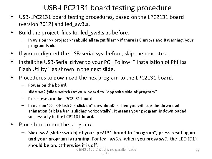
USB-LPC 2131 board testing procedure • USB-LPC 2131 board testing procedures, based on the LPC 2131 board (version 2012) and led_sw 3. s. • Build the project files for led_sw 3. s as before. – In uvision 4>> project >>rebuild all target files>> if there is 0 errors and 0 warning, your program is ok. • If you configured the USB-serial sys. before, skip the next step. • Install the USB-Serial driver to your PC: Follow " Installation of Philips Flash Utility " as shown in the next slide. • Procedures to download the hex program to the LPC 2131 board. – – Power on the board. slide sw 2 (slide switch) of your board to “opposite side of program”. Press reset on the LPC 2131 board. In uvision 4>> >>Flash >>”click on” download>> Then you will see the download animation (a blue bar is sliding horizontally). It means your program is downloaded successfully to the LCP 2131 board. • Procedure to run the program: – Slide sw 2 (slide switch) of your lpc 2131 board to “program”, press reset again and your program is running. For led_sw 3. s, when you press sw 3, the LED (D 1) should be on. Otherwise it is off. CENG 2400 Ch 7: driving parallel loads v. 7 a 47

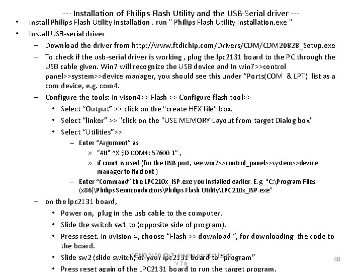
• • --- Installation of Philips Flash Utility and the USB-Serial driver --- Install Philips Flash Utility Installation. run " Philips Flash Utility Installation. exe " Install USB-serial driver – Download the driver from http: //www. ftdichip. com/Drivers/CDM 20828_Setup. exe – To check if the usb-serial driver is working , plug the lpc 2131 board to the PC through the USB cable given. Win 7 will recognize the USB device and In win 7>>control panel>>system>>device manager, you should see this under “Ports(COM & LPT) list as a com device, e. g. com 4. – Configure the tools: In vison 4>> Flash >> Configure flash tool>> • Select “Output” >> click on the "create HEX file" box. • Select “linker” >> "click on the "USE MEMORY Layout from target Dialog box" • Select “Utilities”>> – Enter “Argument” as » "#H" ^X $D COM 4: 57600 1” , » if com 4 is used (for the USB port, see win 7>>control_panel>>system>>device manager to find out ) – Enter “Command” the LPC 210 x_ISP. exe you installed earlier. E. g. “C: Program Files (x 86)Philips SemiconductorsPhilips Flash UtilityLPC 210 x_ISP. exe” – on the lpc 2131 board, • Power on, plug in the usb cable to the computer. • Slide the switch sw 1 to (opposite side of program). • Press reset. In uvision 4, choose “Flash >> download “, for downloading the code to the board. CENG 2400 driving parallel • Slide sw 2 (slide switch) of your Ch 7: lpc 2131 board toloads “program” 48 v. 7 a • Press reset again of the LPC 2131 board to run the target program.

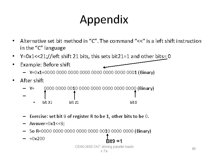
Appendix • Alternative set bit method in “C”. The command “<<“ is a left shift instruction in the “C” language • Y=0 x 1<<21; //left shift 21 bits, this sets bit 21=1 and other bits= 0 • Example: Before shift – Y=0 x 1=0000 0000 0001 (Binary) • After shift – Y= – • – – 0000 0010 0000 0000 (Binary) bit 31 bit 21 bit 0 Exercise: set bit 9 of register R to be 1, other bits to be 0. Answer=0 x 1<<9; So R=0000 0000 0010 0000 (Binary) =0 x 200 Bit 9 =1 CENG 2400 Ch 7: driving parallel loads v. 7 a 49

Software solution debounce 1. c • • • • • #include <lpc 213 x. h> //debounce 1. c #define RED_LED 0 x 00000400 //set p 0. 10 as RED LED #define SW 3 0 x 00100000 //set p 0. 20 as SW 3 int main(void) { long tmp; // variable for temporary storage of port 0 status int flag; IO 0 DIR = RED_LED; // set p 0. 10 as output tmp = IO 0 PIN & SW 3; // read SW 3 (p 0. 20) while(1) { while(tmp==0) tmp = IO 0 PIN & SW 3; // wait SW 3 (p 0. 20) change to high while(tmp!=0) tmp = IO 0 PIN & SW 3; // wait SW 3 (p 0. 20) change to low if(flag==0) { flag = 1; IO 0 SET = RED_LED; //turn on LED } else { flag = 0; IO 0 CLR = RED_LED; //turn off LED } } CENG 2400 Ch 7: driving parallel loads } v. 7 a 50