Chapter 7 Cosimulation of chip package and board

Chapter 7 Co-simulation of chip, package and board Prof. Lei He Electrical Engineering Department University of California, Los Angeles URL: eda. ee. ucla. edu Email: lhe@ee. ucla. edu

Why do We Need Co-Simulation? q Thermal/power/electrical Coupling Ø leakage power in a semiconductor device depends on the local temperatures of individual cells q Ø temperature distributions also depend on leakage power distributions Ø temperature dependence of a metal’s electrical conductivity Ø Joule heating (or self-heating) of metals with currents flowing through Integrated RDL, package, and board model Ø Increasingly, package and system designers have started to include RDL traces in package models because in today’s designs RDL and package traces are so close to each other that coupling between them is significant. 2

3

Importance of Co-Simulation A differential pair from chip to package to board Comparison of s-parameter results between segregated and integrated models Figures obtained from An-Yu Kuo, Apache Design Solutions 4

Organization q q Chip Modeling Ø IBIS Ø CPM Package and Board Modeling Ø S Parameters http: //www. polarinstruments. com/support/cits/s_parameters. ppt q Co-simulation Flow

Simulation Models: SPICE Ø Ø SPICE simulations model a circuit at transistor level, thus SPICE models contain detailed information about the circuit and process parameters which is regarded as proprietary and IC vendors are reluctant to provide. . Not all SPICE simulators are fully compatible. Although SPICE simulation accuracy is typically very good, a significant limitation with this type of modeling is simulation speed. SPICE has various simulator options that control accuracy, convergence and the algorithm type, and any options that are not consistent might give rise to poor correlation in simulation results across different simulators. IBIS, is an alternative to SPICE simulation.

What Is IBIS? I I/O B Buffer I Information S Specification http: //www. eigroup. org/ibis/ http: //www. ibis-information. org/ Ø IBIS is a universal standard for describing the analog behavior of digital device buffers using data in ASCII text format IBIS files are not really models, they just contain the data that will be used by the simulation tool’s behavioral models and algorithms Ø Started in the early 90 s to promote tool-independent I/O models for system-level signal integrity work Ø IBIS 3. 2 is standardized: ANSI/EIA-656 -A and IEC 62014 -1 Ø IBIS 4. 1 incorporates links to VHDL-AMS and Verilog-AMS

Simulation Models: IBIS ØIBIS behavioral data is taken from actual devices. ØIBIS models tend to simulate much faster than SPICE models. ØIBIS Modeling provides a simple table-based buffer model for semiconductor devices. ØIBIS models can be used to characterize I/V output curves, rising/falling transition waveforms, and package parasitic information of the device. ØIBIS models are intended to provide nonproprietary information about I/O buffers and are more easily available from different IC vendors ØNon-convergence is eliminated in IBIS simulation. ØVirtually all EDA vendors presently support IBIS models, and ease of use of these IBIS simulators is generally very good. ØIBIS models for most devices are freely available over the Internet making it easy to simulate several different manufacturers’ devices on the same board.
![Elements of an IBIS Model [2] [3] [4] [5] [1]](http://slidetodoc.com/presentation_image_h2/33729510205733d873cb07cf67cb22d1/image-9.jpg "Elements of an IBIS Model [2] [3] [4] [5] [1]")
Elements of an IBIS Model [2] [3] [4] [5] [1]

Elements of an IBIS Model Element 1: Pull-down 4 Describes the I/V characteristics during pull-down. 4 Data for minimum and maximum current for given voltages. 4 Data is taken for -Vcc to 2 Vcc as that allows a behavioral model for signal reflections caused by improper termination and overshoot and undershoot situations when the protection diodes are forward biased. Element [1]

Elements of an IBIS Model Element 2: Pull-up 4 Describes the pull-up state of the buffer when the output drives high. 4 Data is entered using the formula Vtable = Vcc – Voutput 4 The minimum and maximum values are determined by the minimum and maximum operating temperatures, supply voltages and process variations. 4 Combining the highest current values with the fastest ramp time and minimum package characteristics, a fast model can be derived. A slow model can be derived by combining the lowest current with the slowest ramp time and maximum package characteristics. Element [2]

Elements of an IBIS Model Element 3: GND and Power Clamps 4 Describes the ground and power clamp diodes. 4 The GND clamp curve is derived from the ground relative data gathered while the buffer is in the high-impedance state and illustrates the region where the ground clamp diode is active. The range is from -Vcc to Vcc. 4 The power clamp curve is derived from the Vcc relative data gathered while the buffer is in a high impedance state and shows the region where the power clamp diode is active. This measurement ranges from Vcc to 2 Vcc. Element [3]

Elements of an IBIS Model Element 4: Ramp 4 Describes the ramp time for the pull-up and pull-down devices. Ensures proper AC operation of the model. 4 The min and max columns represent the minimum and maximum slew rates for the buffers. 4 The values represent the intrinsic values of the transistors with all package parasitics and external loads removed. Element [4]

Elements of an IBIS Model Element 5: Package 4 Adds the component and package parasitics. 4 C_comp is the capacitance of the die itself, excluding the package capacitance. 4 Package characteristic resistance, inductance and capacitance are added by R_pkg, L_pkg, and C_pkg, respectively. Element [5] 14

Putting it all together – the IBIS File A standard IBIS model file consists of three sections: ØHeader Info Ø basic information about the IBIS file and what data it provides. ØComponent, Package, and Pin Info Ø the targeted device package, pin lists, pin operating conditions, and pin-to-buffer mapping. ØV-I Behavioral Model Ø all data to recreate I-V curves as well as V-t transition waveforms, which describe the switching properties of the particular buffer.

Chip Power Network Model Traditional model Ø This simplified model of the die’s power delivery network can result in inaccurate global power analysis ü die current can influence the voltage drop through the system ü the resistive and capacitive components of the die can determine the resonance frequency and its amplitude. 16

Chip Power Network Model CPM Model from Apache Ø CPM contains current sources and R, L, and C parasitics. Ø It provides a reduced view of effective Rdie and Cdie for different frequencies of operation. Ø It also provides switching current that varies over time and space 17

Organization q q Chip Modeling Ø IBIS Ø CPM Package and Board Modeling Ø q S Parameters Co-simulation Flow

Black Box Representation Ø S-parameters are a useful method for representing a circuit as a “black box” Ø The external behaviour of this black box can be predicted without any regard for the contents of the black box. ü a resistor ü a transmission line ü an integrated circuit.

Definition of Ports A “black box” or network may have any number of ports. This diagram shows a simple network with just 2 ports. Note : A port is a terminal pair of lines.

S Parameter Definition S-parameters are measured by sending a single frequency signal into the network or “black box” and detecting what waves exit from each port. Power, voltage and current can be considered to be in the form of waves travelling in both directions. For a wave incident on Port 1, some part of this signal reflects back out of that port and some portion of the signal exits other ports.

Explanation of S Parameters For a two-port system: First lets look at S 11 refers to the signal reflected at Port 1 for the signal incident at Port 1. Scattering parameter S 11 is the ratio of the two waves b 1/a 1.

Explanation of S Parameters For a two-port system: Now lets look at S 21 refers to the signal exiting at Port 2 for the signal incident at Port 1. Scattering parameter S 21 is the ratio of the two waves b 2/a 1.

Explanation of S Parameters For a two-port system: Now lets look at S 21 refers to the signal exiting at Port 2 for the signal incident at Port 1. Scattering parameter S 21 is the ratio of the two waves b 2/a 1. S 21? Surely that should be S 12? ? S 21 is correct! S-parameter convention always refers to the responding port first!

Explanation of S Parameters

Explanation of S Parameters A linear network can be characterised by a set of simultaneous equations describing the exiting waves from each port in terms of incident waves. S 11 = b 1 / a 1 S 12 = b 1 / a 2 S 21 = b 2 / a 1 S 22 = b 2 / a 2 Note again how the subscript follows the parameters in the ratio (S 11=b 1/a 1, etc. . . )

Explanation of S Parameters
")
Explanation of S Parameters S-parameters are complex (i. e. they have magnitude and angle) because both the magnitude and phase of the input signal are changed by the network. (This is why they are sometimes referred to as complex scattering parameters). These four S-parameters actually contain eight separate numbers: the real and imaginary parts (or the modulus and the phase angle) of each of the four complex scattering parameters. Quite often we refer to the magnitude only as it is of the most interest. How much gain (or loss) you get is usually more important than how much the signal has been phase shifted.

What do S-parameters depend on? S-parameters depend upon the network and the characteristic impedances of the source and load used to measure it, and the frequency measured at. i. e. if the network is changed, the S-parameters change. if the frequency is changed, the S-parameters change. if the load impedance is changed, the S-parameters change. In the Si 9000 e S-parameters are quoted with source and load impedances of 50 Ohms if the source impedance is changed, the S-parameters change.

A little math… This is the matrix algebraic representation of 2 port S-parameters: Some matrices are symmetrical. A symmetrical matrix has symmetry about the leading diagonal. In the case of a 2 -port network, that means that S 21 = S 12 and interchanging the input and output ports does not change the transmission properties. A transmission line is an example of a symmetrical 2 -port network.

Ø Parameters along the leading diagonal, S 11 & S 22, of the S-matrix are referred to as reflection coefficients because they refer to the reflection occurring at one port only. Ø Off-diagonal S-parameters, S 12, S 21, are referred to as transmission coefficients because they refer to what happens from one port to another.

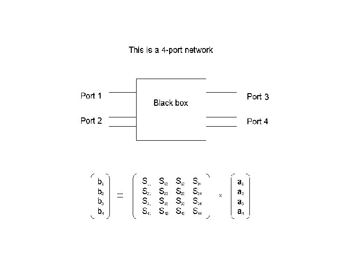
How about Larger networks: Ø A Network may have any number of ports. . . Ø The S-matrix for an n-port network contains n 2 coefficients (Sparameters), each one representing a possible input-output path. Ø The number of rows and columns in an S-parameters matrix is equal to the number of ports. Ø For the S-parameter subscripts “ij”, “j” is the port that is excited (the input port) and “i” is the output port. Yes i for output j for input — logical ; -)

Sum up … ØS-parameters are a powerful way to describe an electrical network ØS-parameters change with frequency / load impedance / source impedance / network ØS 11 is the reflection coefficient ØS 21 describes the forward transmission coefficient (responding port 1 st!) ØS-parameters have both magnitude and phase information ØSometimes the gain (or loss) is more important than the phase shift and the phase information may be ignored ØS-parameters may describe large and complex networks

Organization q q Chip Modeling Ø IBIS Ø CPM Package and Board Modeling Ø q S Parameters Co-simulation Flow

Co-Simulation Flow Frequency domain CPM/IBIS model in s domain for circuits S parameters for package/board Time domain CPM/IBIS model for circuits Ckt realization of S parameters for package/board IFFT 36
- Slides: 36