CHAPTER 6 VOLTAGE REGULATOR Tulus Ikhsan Nasution POWER
- Slides: 31

CHAPTER 6 VOLTAGE REGULATOR Tulus Ikhsan Nasution

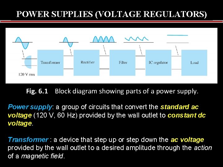
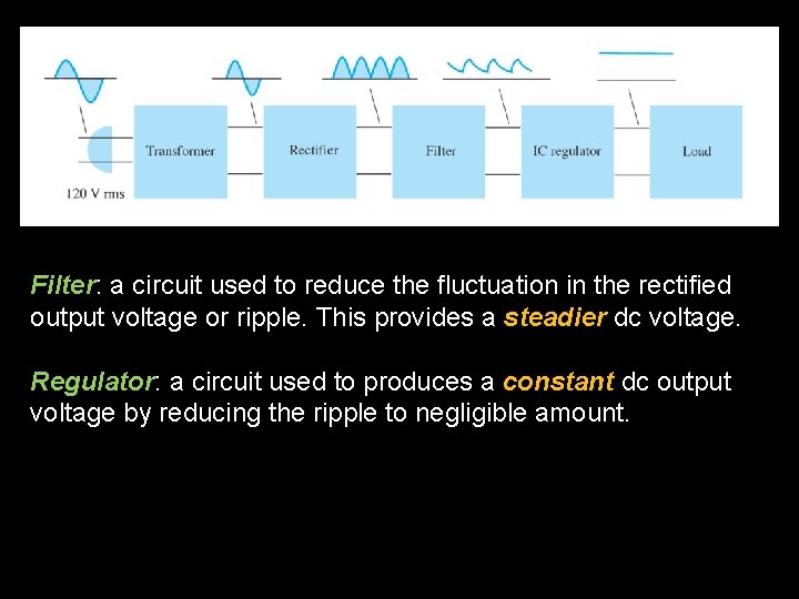
POWER SUPPLIES (VOLTAGE REGULATORS) Fig. 6. 1 Block diagram showing parts of a power supply. Power supply: supply a group of circuits that convert the standard ac voltage (120 V, 60 Hz) provided by the wall outlet to constant dc voltage. Transformer : a device that step up or step down the ac voltage provided by the wall outlet to a desired amplitude through the action of a magnetic field.

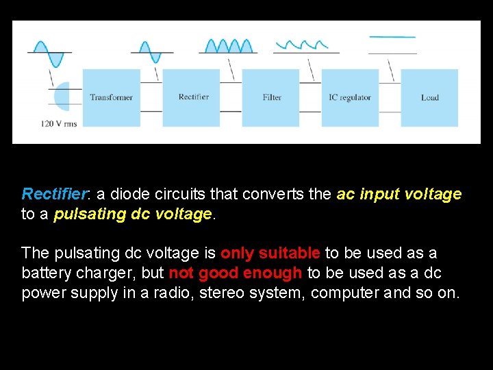
Rectifier: Rectifier a diode circuits that converts the ac input voltage to a pulsating dc voltage. The pulsating dc voltage is only suitable to be used as a battery charger, but not good enough to be used as a dc power supply in a radio, stereo system, computer and so on.

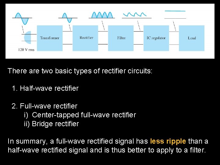
There are two basic types of rectifier circuits: 1. Half-wave rectifier 2. Full-wave rectifier i) Center-tapped full-wave rectifier ii) Bridge rectifier In summary, a full-wave rectified signal has less ripple than a half-wave rectified signal and is thus better to apply to a filter.

Filter: Filter a circuit used to reduce the fluctuation in the rectified output voltage or ripple. This provides a steadier dc voltage. Regulator: Regulator a circuit used to produces a constant dc output voltage by reducing the ripple to negligible amount.

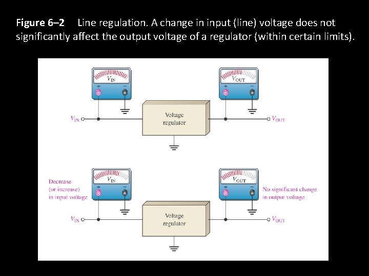
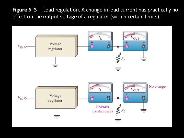
VOLTAGE REGULATION Two basic categories of voltage regulation are: q line regulation; q load regulation. The purpose of line regulation is to maintain a nearly constant output voltage when the input voltage varies. The purpose of load regulation is to maintain a nearly constant output voltage when the load varies.

Figure 6– 2 Line regulation. A change in input (line) voltage does not significantly affect the output voltage of a regulator (within certain limits).

Figure 6– 3 Load regulation. A change in load current has practically no effect on the output voltage of a regulator (within certain limits).

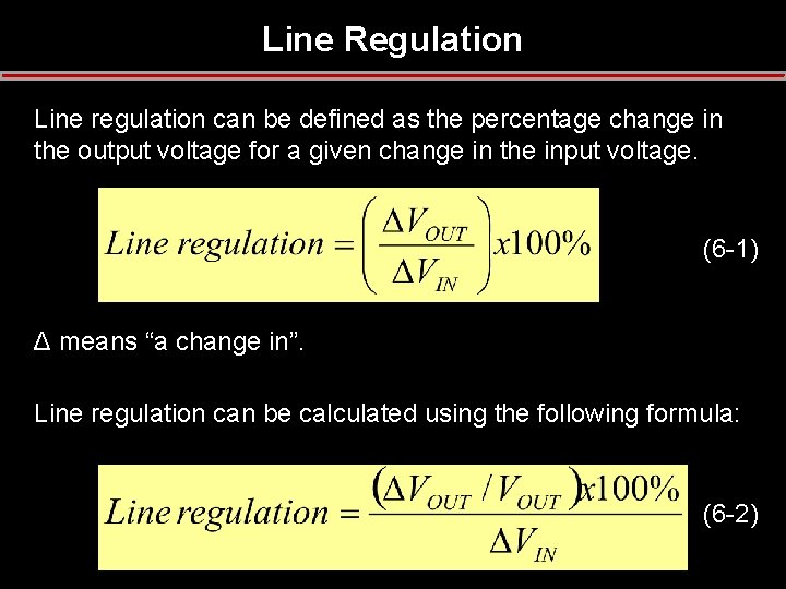
Line Regulation Line regulation can be defined as the percentage change in the output voltage for a given change in the input voltage. (6 -1) Δ means “a change in”. Line regulation can be calculated using the following formula: (6 -2)

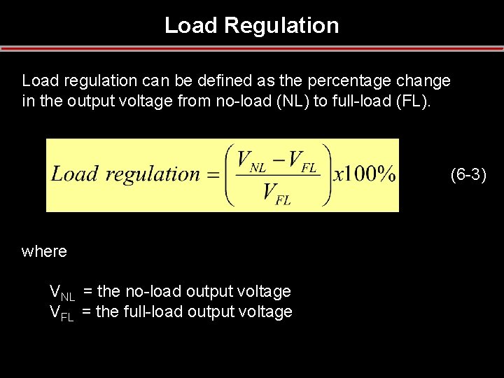
Load Regulation Load regulation can be defined as the percentage change in the output voltage from no-load (NL) to full-load (FL). (6 -3) where VNL = the no-load output voltage VFL = the full-load output voltage

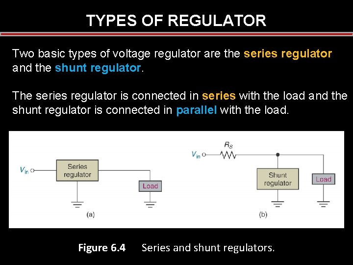
TYPES OF REGULATOR Two basic types of voltage regulator are the series regulator and the shunt regulator. The series regulator is connected in series with the load and the shunt regulator is connected in parallel with the load. Figure 6. 4 Series and shunt regulators.

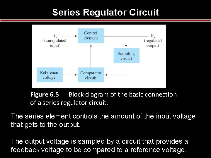
Series Regulator Circuit Figure 6. 5 Block diagram of the basic connection of a series regulator circuit. The series element controls the amount of the input voltage that gets to the output. The output voltage is sampled by a circuit that provides a feedback voltage to be compared to a reference voltage.

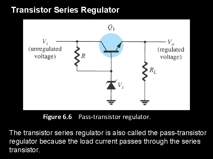
Transistor Series Regulator Figure 6. 6 Pass-transistor regulator. The transistor series regulator is also called the pass-transistor regulator because the load current passes through the series transistor.

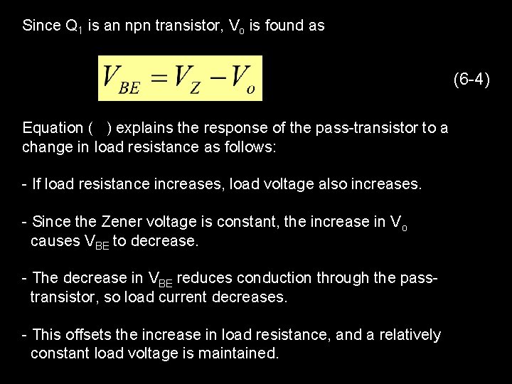
Since Q 1 is an npn transistor, Vo is found as (6 -4) Equation ( ) explains the response of the pass-transistor to a change in load resistance as follows: - If load resistance increases, load voltage also increases. - Since the Zener voltage is constant, the increase in Vo causes VBE to decrease. - The decrease in VBE reduces conduction through the passtransistor, so load current decreases. - This offsets the increase in load resistance, and a relatively constant load voltage is maintained.

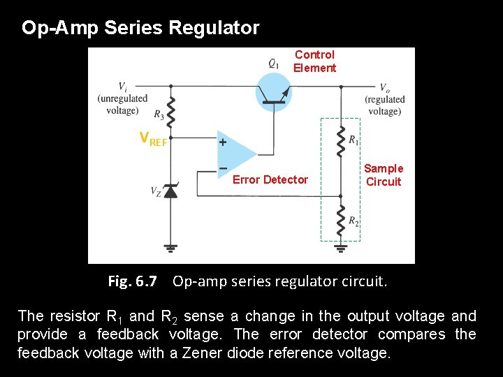
Op-Amp Series Regulator Control Element VREF Error Detector Sample Circuit Fig. 6. 7 Op-amp series regulator circuit. The resistor R 1 and R 2 sense a change in the output voltage and provide a feedback voltage. The error detector compares the feedback voltage with a Zener diode reference voltage.

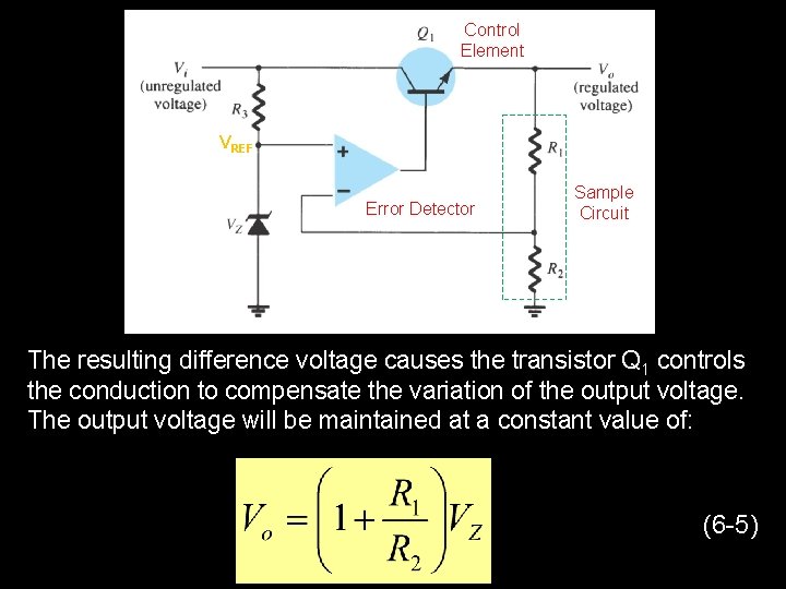
Control Element VREF Error Detector Sample Circuit The resulting difference voltage causes the transistor Q 1 controls the conduction to compensate the variation of the output voltage. The output voltage will be maintained at a constant value of: (6 -5)

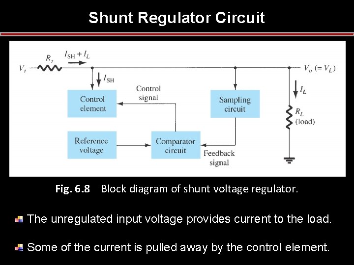
Shunt Regulator Circuit Fig. 6. 8 Block diagram of shunt voltage regulator. The unregulated input voltage provides current to the load. Some of the current is pulled away by the control element.

If the load voltage tries to change due to a change in the load resistance, the sampling circuit provides a feedback signal to a comparator. The resulting difference voltage then provides a control signal to vary the amount of the current shunted away from the load to maintain the regulated output voltage across the load.

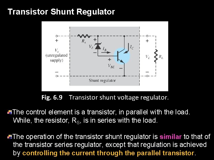
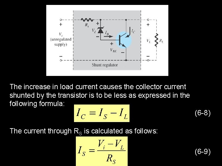
Transistor Shunt Regulator Fig. 6. 9 Transistor shunt voltage regulator. The control element is a transistor, in parallel with the load. While, the resistor, RS, is in series with the load. The operation of the transistor shunt regulator is similar to that of the transistor series regulator, except that regulation is achieved by controlling the current through the parallel transistor.

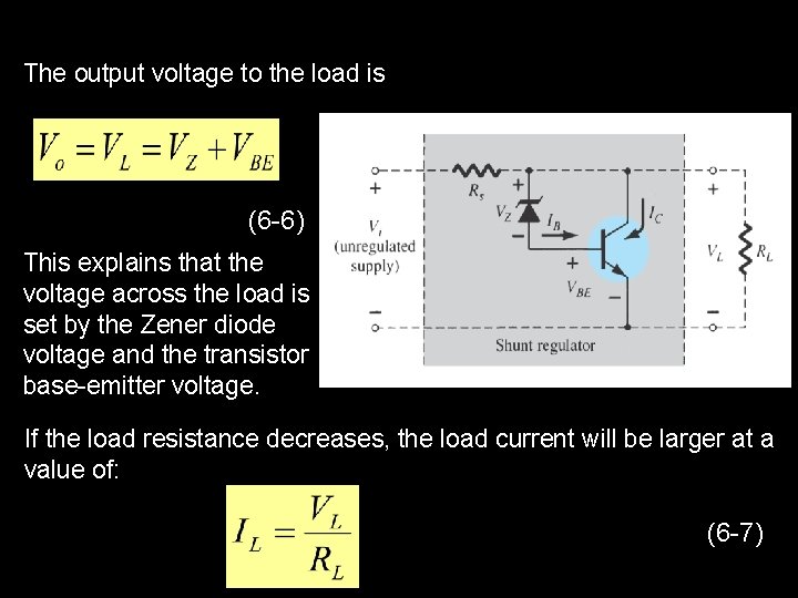
The output voltage to the load is (6 -6) This explains that the voltage across the load is set by the Zener diode voltage and the transistor base-emitter voltage. If the load resistance decreases, the load current will be larger at a value of: (6 -7)

The increase in load current causes the collector current shunted by the transistor is to be less as expressed in the following formula: (6 -8) The current through RS is calculated as follows: (6 -9)

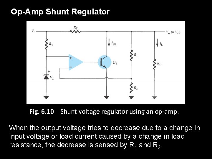
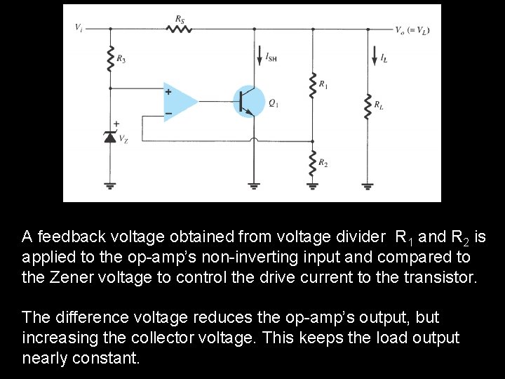
Op-Amp Shunt Regulator Fig. 6. 10 Shunt voltage regulator using an op-amp. When the output voltage tries to decrease due to a change in input voltage or load current caused by a change in load resistance, the decrease is sensed by R 1 and R 2.

A feedback voltage obtained from voltage divider R 1 and R 2 is applied to the op-amp’s non-inverting input and compared to the Zener voltage to control the drive current to the transistor. The difference voltage reduces the op-amp’s output, but increasing the collector voltage. This keeps the load output nearly constant.

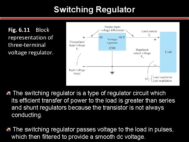
Switching Regulator Fig. 6. 11 Block representation of three-terminal voltage regulator. The switching regulator is a type of regulator circuit which its efficient transfer of power to the load is greater than series and shunt regulators because the transistor is not always conducting. The switching regulator passes voltage to the load in pulses, which then filtered to provide a smooth dc voltage.

IC VOLTAGE REGULATORS Several types of both linear (series and shunt) and switching regulators are available in integrated circuit (IC) form. Single IC regulators contain the circuitry for: (1) reference source, (2) comparator amplifier, (3) control device, and; (4) overload protection. Generally, the linear regulators are three-terminal devices that provides either positive or negative output voltages that can be either fixed or adjustable.

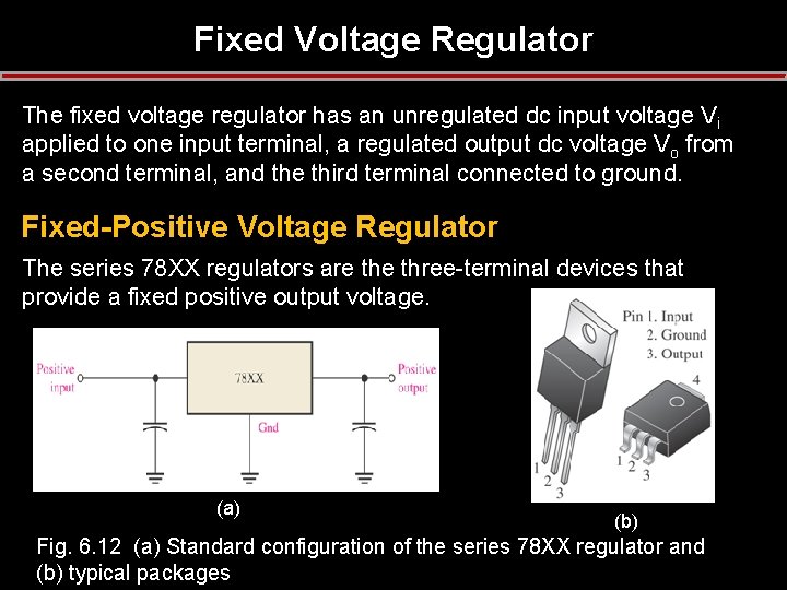
Fixed Voltage Regulator The fixed voltage regulator has an unregulated dc input voltage Vi applied to one input terminal, a regulated output dc voltage Vo from a second terminal, and the third terminal connected to ground. Fixed-Positive Voltage Regulator The series 78 XX regulators are three-terminal devices that provide a fixed positive output voltage. (a) (b) Fig. 6. 12 (a) Standard configuration of the series 78 XX regulator and (b) typical packages

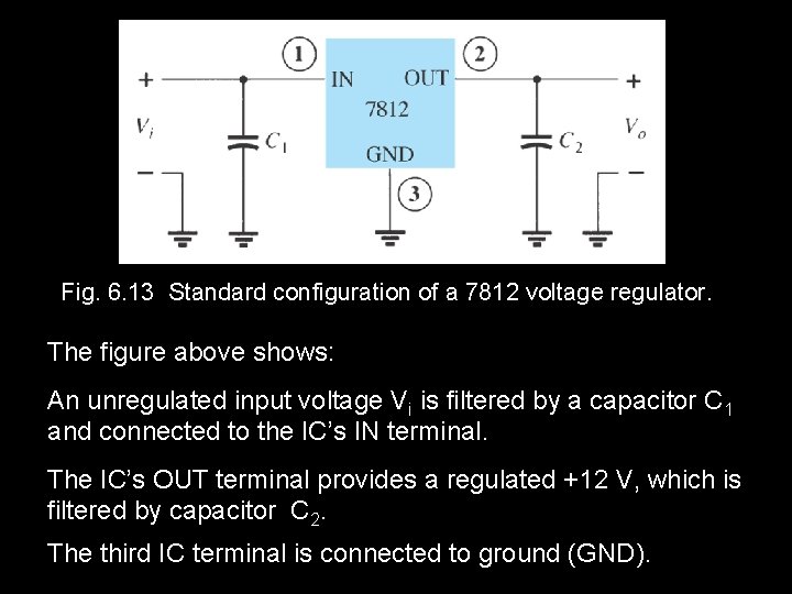
Fig. 6. 13 Standard configuration of a 7812 voltage regulator. The figure above shows: An unregulated input voltage Vi is filtered by a capacitor C 1 and connected to the IC’s IN terminal. The IC’s OUT terminal provides a regulated +12 V, which is filtered by capacitor C 2. The third IC terminal is connected to ground (GND).

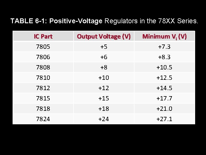
TABLE 6 -1: Positive-Voltage Regulators in the 78 XX Series. IC Part 7805 7806 7808 Output Voltage (V) +5 +6 +8 Minimum Vi (V) +7. 3 +8. 3 +10. 5 7810 7812 7815 7818 7824 +10 +12 +15 +18 +24 +12. 5 +14. 5 +17. 7 +21. 0 +27. 1

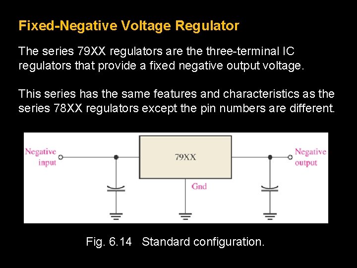
Fixed-Negative Voltage Regulator The series 79 XX regulators are three-terminal IC regulators that provide a fixed negative output voltage. This series has the same features and characteristics as the series 78 XX regulators except the pin numbers are different. Fig. 6. 14 Standard configuration.

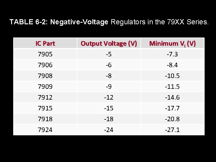
TABLE 6 -2: Negative-Voltage Regulators in the 79 XX Series. IC Part 7905 7906 7908 Output Voltage (V) -5 -6 -8 Minimum Vi (V) -7. 3 -8. 4 -10. 5 7909 7912 7915 7918 7924 -9 -12 -15 -18 -24 -11. 5 -14. 6 -17. 7 -20. 8 -27. 1

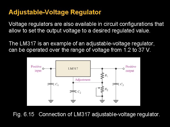
Adjustable-Voltage Regulator Voltage regulators are also available in circuit configurations that allow to set the output voltage to a desired regulated value. The LM 317 is an example of an adjustable-voltage regulator, can be operated over the range of voltage from 1. 2 to 37 V. Fig. 6. 15 Connection of LM 317 adjustable-voltage regulator.