Chapter 6 Static CMOS Circuits Boonchuay Supmonchai Integrated
Chapter 6 Static CMOS Circuits Boonchuay Supmonchai Integrated Design Application Research (IDAR) Laboratory August , 2004; Revised - June 28, 2005 2102 -545 Digital ICs
B. Supmonchai Goals of This Chapter q In-depth discussion of CMOS logic families § Static and Dynamic § Pass-Transistor § Nonratioed and Ratioed Logic q Optimizing gate metrics § Area, Speed, Energy or Robustness q High Performance circuit-design techniques 2102 -545 Digital ICs Static CMOS Circuits 2
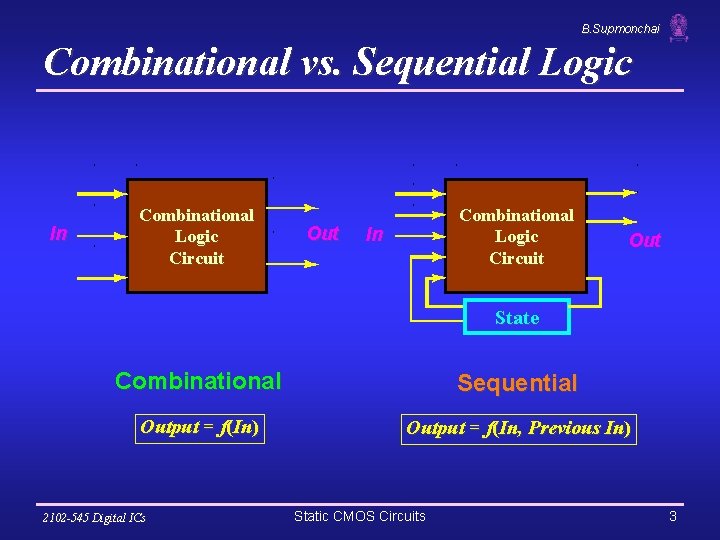
B. Supmonchai Combinational vs. Sequential Logic In Combinational Logic Circuit Out Combinational Logic Circuit In Out State Combinational Sequential Output = f(In) Output = f(In, Previous In) 2102 -545 Digital ICs Static CMOS Circuits 3
B. Supmonchai Static CMOS Circuits q q q At every point in time (except during the switching transients) each gate output is connected to either VDD or VSS via a low-resistance path. The outputs of the gates assume at all times the value of the Boolean function, function implemented by the circuit (ignoring, once again, the transient effects during switching periods) This is in contrast to the dynamic circuit class, which relies on temporary storage of signal values on the capacitance of high impedance circuit nodes 2102 -545 Digital ICs Static CMOS Circuits 4
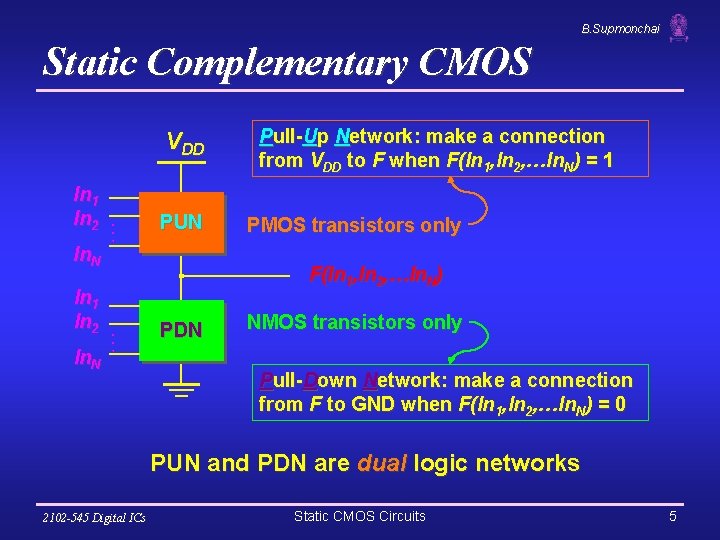
B. Supmonchai Static Complementary CMOS VDD In. N PUN PMOS transistors only F(In 1, In 2, …In. N) … In 1 In 2 Pull-Up Network: make a connection from VDD to F when F(In 1, In 2, …In. N) = 1 PDN NMOS transistors only Pull-Down Network: make a connection from F to GND when F(In 1, In 2, …In. N) = 0 PUN and PDN are dual logic networks 2102 -545 Digital ICs Static CMOS Circuits 5
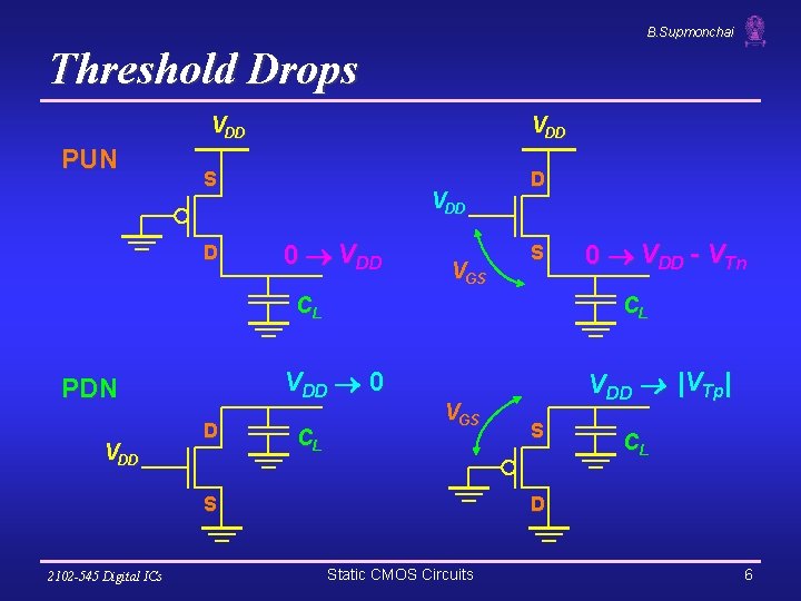
B. Supmonchai Threshold Drops VDD PUN VDD S D VDD 0 VDD VGS D S CL VDD 0 PDN D CL VGS S 2102 -545 Digital ICs 0 VDD - VTn VDD |VTp| S CL D Static CMOS Circuits 6
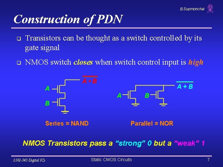
B. Supmonchai Construction of PDN q q Transistors can be thought as a switch controlled by its gate signal NMOS switch closes when switch control input is high A • B A A+B A B B Series = NAND Parallel = NOR NMOS Transistors pass a “strong” 0 but a “weak” 1 2102 -545 Digital ICs Static CMOS Circuits 7
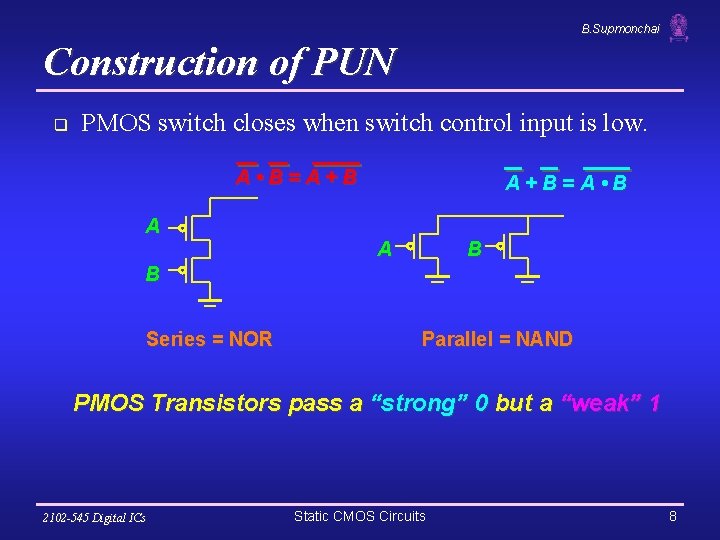
B. Supmonchai Construction of PUN q PMOS switch closes when switch control input is low. A • B=A+B A A+B=A • B A B B Series = NOR Parallel = NAND PMOS Transistors pass a “strong” 0 but a “weak” 1 2102 -545 Digital ICs Static CMOS Circuits 8
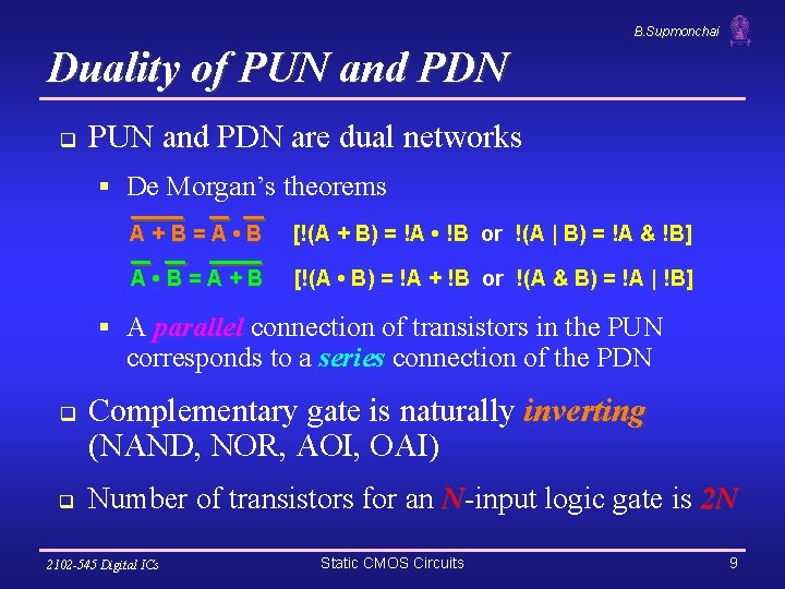
B. Supmonchai Duality of PUN and PDN q PUN and PDN are dual networks § De Morgan’s theorems A+B=A • B [!(A + B) = !A • !B or !(A | B) = !A & !B] A • B=A+B [!(A • B) = !A + !B or !(A & B) = !A | !B] § A parallel connection of transistors in the PUN corresponds to a series connection of the PDN q q Complementary gate is naturally inverting (NAND, NOR, AOI, OAI) Number of transistors for an N-input logic gate is 2 N 2102 -545 Digital ICs Static CMOS Circuits 9

B. Supmonchai Example: CMOS NAND gate VDD A A B B A • B A B F 0 0 1 1 1 0 PDN: G = A · B Conduction to GND PUN: F = A + B Conduction to VDD G(In 1, In 2, …, In. N) = F(In 1, In 2, …, In. N) 2102 -545 Digital ICs Static CMOS Circuits 10
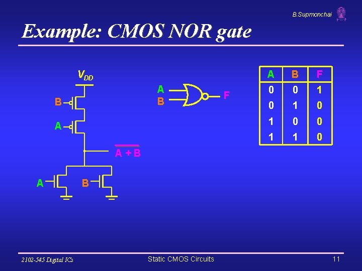
B. Supmonchai Example: CMOS NOR gate VDD A B B A F A B F 0 0 1 0 1 0 0 1 1 0 A+B A 2102 -545 Digital ICs B Static CMOS Circuits 11
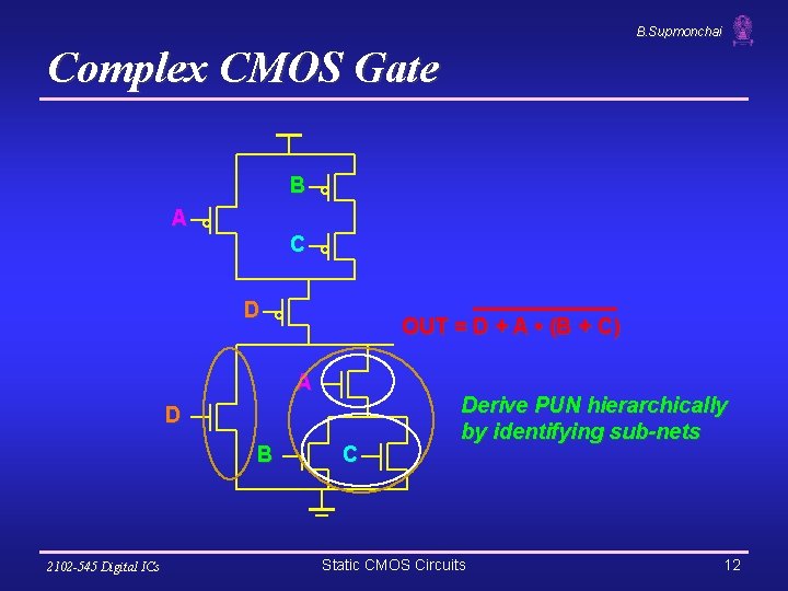
B. Supmonchai Complex CMOS Gate B A C D OUT = D + A • (B + C) A D B 2102 -545 Digital ICs C Derive PUN hierarchically by identifying sub-nets Static CMOS Circuits 12
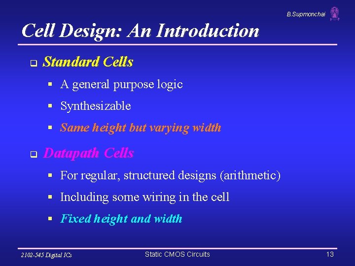
B. Supmonchai Cell Design: An Introduction q Standard Cells § A general purpose logic § Synthesizable § Same height but varying width q Datapath Cells § For regular, structured designs (arithmetic) § Including some wiring in the cell § Fixed height and width 2102 -545 Digital ICs Static CMOS Circuits 13
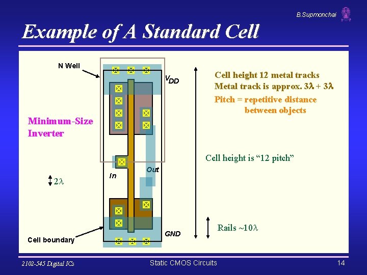
B. Supmonchai Example of A Standard Cell N Well VDD Minimum-Size Inverter Cell height 12 metal tracks Metal track is approx. 3 + 3 Pitch = repetitive distance between objects Cell height is “ 12 pitch” 2 Cell boundary 2102 -545 Digital ICs In Out GND Static CMOS Circuits Rails ~10 14
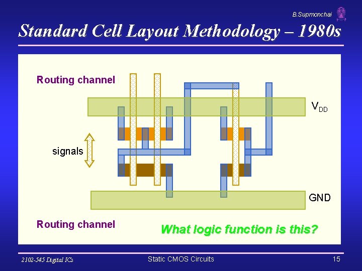
B. Supmonchai Standard Cell Layout Methodology – 1980 s Routing channel VDD signals GND Routing channel 2102 -545 Digital ICs What logic function is this? Static CMOS Circuits 15
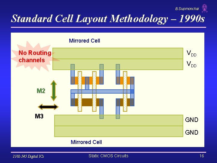
B. Supmonchai Standard Cell Layout Methodology – 1990 s Mirrored Cell No Routing channels VDD M 2 M 3 GND Mirrored Cell 2102 -545 Digital ICs Static CMOS Circuits 16
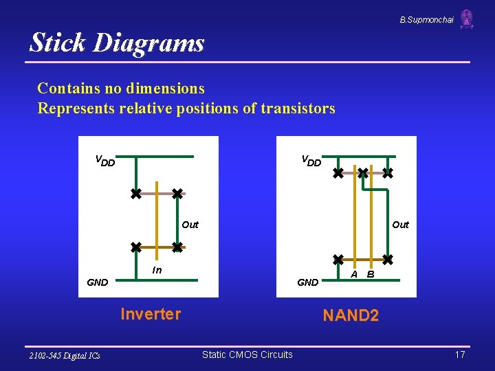
B. Supmonchai Stick Diagrams Contains no dimensions Represents relative positions of transistors VDD Out In GND Inverter 2102 -545 Digital ICs A B NAND 2 Static CMOS Circuits 17
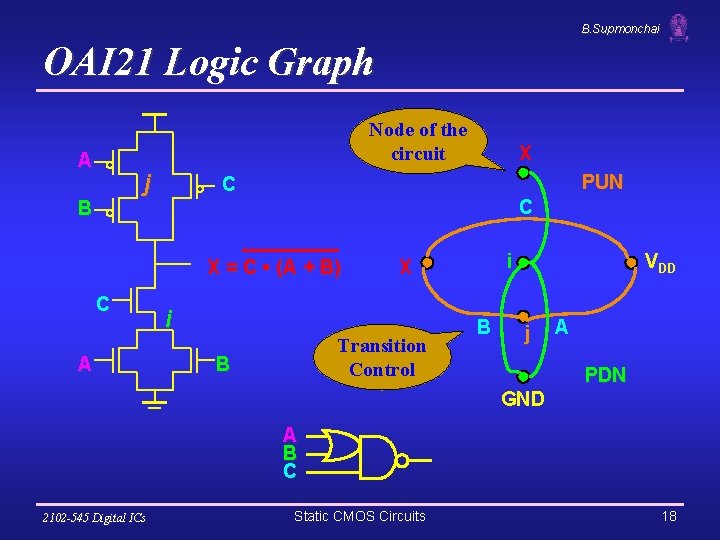
B. Supmonchai OAI 21 Logic Graph Node of the circuit A j B PUN C C X = C • (A + B) C A X i Transition Control B i X B VDD j A PDN GND A B C 2102 -545 Digital ICs Static CMOS Circuits 18
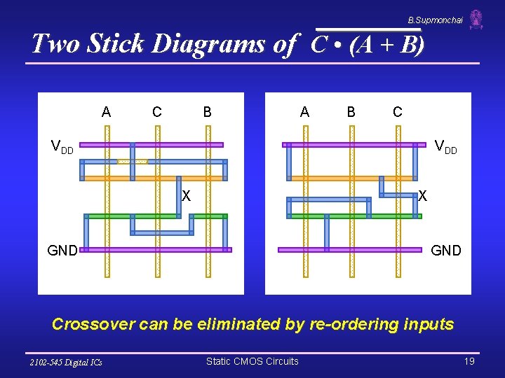
B. Supmonchai Two Stick Diagrams of C • (A + B) A C B A B C VDD X X GND Crossover can be eliminated by re-ordering inputs 2102 -545 Digital ICs Static CMOS Circuits 19
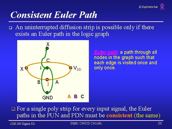
B. Supmonchai Consistent Euler Path q An uninterrupted diffusion strip is possible only if there exists an Euler path in the logic graph X C X i B VDD j GND Euler path: a path through all nodes in the graph such that each edge is visited once and only once. A A B C q For a single poly strip for every input signal, the Euler paths in the PUN and PDN must be consistent (the same) 2102 -545 Digital ICs Static CMOS Circuits 20
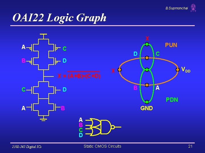
B. Supmonchai OAI 22 Logic Graph X A B PUN C D D X = (A+B) • (C+D) C C VDD X B D A PDN A GND B A B C D 2102 -545 Digital ICs Static CMOS Circuits 21
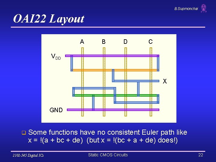
B. Supmonchai OAI 22 Layout A B D C VDD X GND q Some functions have no consistent Euler path like x = !(a + bc + de) (but x = !(bc + a + de) does!) 2102 -545 Digital ICs Static CMOS Circuits 22
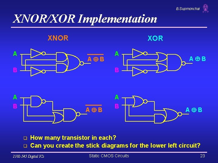
B. Supmonchai XNOR/XOR Implementation XNOR A XOR A B B A B A B q q A B How many transistor in each? Can you create the stick diagrams for the lower left circuit? 2102 -545 Digital ICs Static CMOS Circuits 23
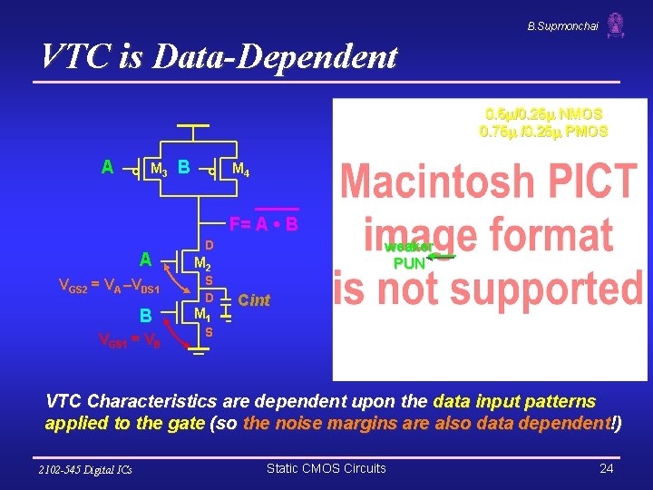
B. Supmonchai VTC is Data-Dependent 0. 5 /0. 25 NMOS 0. 75 /0. 25 PMOS A M 3 B M 4 F= A • B A VGS 2 = VA –VDS 1 B VGS 1 = VB D weaker PUN M 2 S D M 1 Cint S VTC Characteristics are dependent upon the data input patterns applied to the gate (so the noise margins are also data dependent!) 2102 -545 Digital ICs Static CMOS Circuits 24
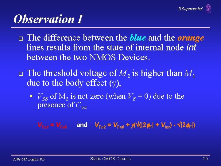
B. Supmonchai Observation I q q The difference between the blue and the orange lines results from the state of internal node int between the two NMOS Devices. The threshold voltage of M 2 is higher than M 1 due to the body effect ( ), § VSB of M 2 is not zero (when VB = 0) due to the presence of Cint VTn 1 = VTn 0 2102 -545 Digital ICs and VTn 2 = VTn 0 + ( (|2 F| + Vint) - |2 F|) Static CMOS Circuits 25
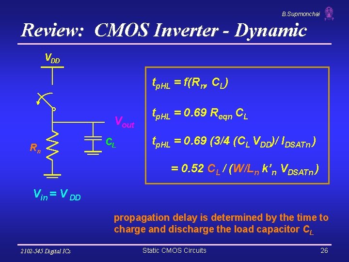
B. Supmonchai Review: CMOS Inverter - Dynamic VDD tp. HL = f(Rn, CL) Vout Rn CL tp. HL = 0. 69 Reqn CL tp. HL = 0. 69 (3/4 (CL VDD)/ IDSATn ) = 0. 52 CL / (W/Ln k’n VDSATn ) Vin = V DD propagation delay is determined by the time to charge and discharge the load capacitor CL 2102 -545 Digital ICs Static CMOS Circuits 26
B. Supmonchai Review: Designing for Performance q Reduce CL q Increase W/L ratio of the transistor § the most powerful and effective performance optimization tool § watch out for self-loading! q Increase VDD § only minimal improvement in performance at the cost of increased energy dissipation q Slope engineering - keeping signal rise and fall times smaller than or equal to the gate propagation delays and of approximately equal values § good for performance and power consumption 2102 -545 Digital ICs Static CMOS Circuits 27
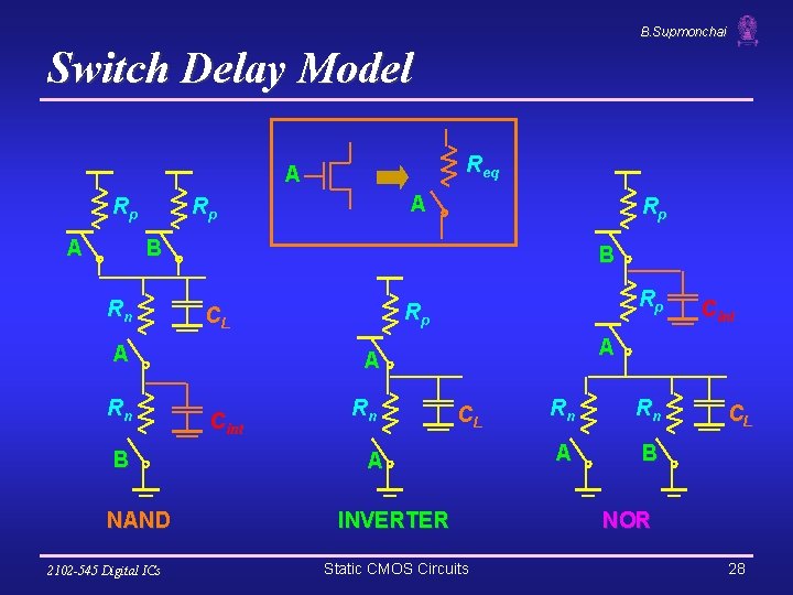
B. Supmonchai Switch Delay Model Req A Rp A A Rp Rp B Rn B CL A Rn B NAND 2102 -545 Digital ICs Rp Rp A A Cint Rn Cint CL A INVERTER Static CMOS Circuits Rn Rn A B CL NOR 28
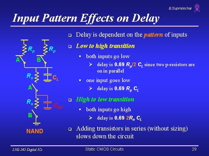
B. Supmonchai Input Pattern Effects on Delay Rp A Rp q Delay is dependent on the pattern of inputs q Low to high transition § both inputs go low B Rn Ø delay is 0. 69 Rp/2 CL since two p-resistors are on in parallel CL § one input goes low A Rn Ø delay is 0. 69 Rp CL Cint q § both inputs go high B NAND 2102 -545 Digital ICs High to low transition Ø delay is 0. 69 2 Rn CL q Adding transistors in series (without sizing) slows down the circuit Static CMOS Circuits 29
![B. Supmonchai Delay Dependence on Input Patterns Voltage [V] A=B=1 0 A=1 0, B=1 B. Supmonchai Delay Dependence on Input Patterns Voltage [V] A=B=1 0 A=1 0, B=1](http://slidetodoc.com/presentation_image_h/f9b7e93ff4a08cc313f27beec4073d98/image-30.jpg)
B. Supmonchai Delay Dependence on Input Patterns Voltage [V] A=B=1 0 A=1 0, B=1 A=1, B=1 0 time [ps] Input Data Delay Pattern (psec) A=B=0 1 67 A=1, B=0 1 64 A= 0 1, B=1 61 A=B=1 0 45 A=1, B=1 0 80 A= 1 0, B=1 81 NMOS = 0. 5 m/0. 25 m, PMOS = 0. 75 m/0. 25 m, CL = 100 f. F 2102 -545 Digital ICs Static CMOS Circuits 30
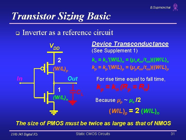
B. Supmonchai Transistor Sizing Basic q Inverter as a reference circuit Device Transconductance VDD (See Supplement 1) kn = kn’(W/L)n = (µn ox/tox)((W/L)n kp = kp’(W/L)p = (µp ox/tox)((W/L)p 2 (W/L)p In Out 1 (W/L)n CL For rise time equal to fall time, k p = k n (R p = R n ) Because µp ~ µn /2 ( W / L )p = 2 (W / L )n The size of PMOS must be twice as large as that of NMOS 2102 -545 Digital ICs Static CMOS Circuits 31
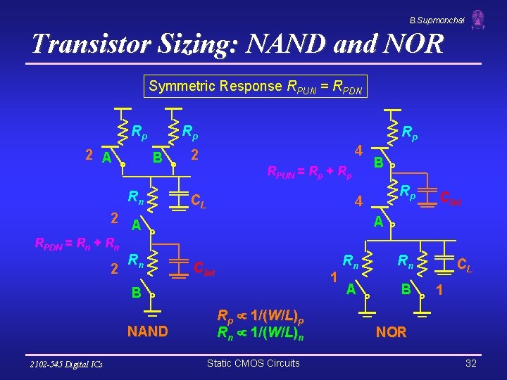
B. Supmonchai Transistor Sizing: NAND and NOR Symmetric Response RPUN = RPDN Rp 2 A Rp B Rn 2 A RPDN = Rn + Rn 2 Rn Rp 4 2 RPUN = Rp + Rp CL 2102 -545 Digital ICs Rp 4 Cint A Cint 1 B NAND B Rp 1/(W/L)p Rn 1/(W/L)n Static CMOS Circuits Rn Rn A B CL 1 NOR 32
B. Supmonchai Note on Transistor Sizing q q By assuming RPUN = RPDN, we ignores the extra diffusion capacitance introduced by widening the transistors. In DSM, even larger increases in the width are needed due to velocity saturation § For 2 -input NANDs, the NMOS transistors should be made 2. 5 times as wide. q NAND implementation is clearly preferred over a NOR implementation, implementation since a PMOS stack series is slower than an NMOS stack due to lower carrier mobility 2102 -545 Digital ICs Static CMOS Circuits 33

B. Supmonchai Transistor Sizing: Complex CMOS Gate q A 46 D B 8 12 C 8 12 § Follow short path first; note PMOS for C and B, 4 rather than 3 (average in pull-up chain of three = (4+4+2)/3) § Also note structure of pull-up and 46 A D Red sizing assuming RPUN = RPDN pull-down to minimize diffusion cap. at output (e. g. , single PMOS drain connected to output) 2 1 q B 2 C 2 Green for symmetric response and for performance (where Rp = 3 Rn) § Sizing rules of thumb: PMOS = 3 * NMOS 2102 -545 Digital ICs Static CMOS Circuits 34
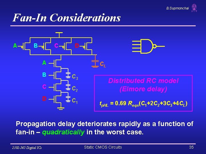
B. Supmonchai Fan-In Considerations A B C D A CL B C 3 C C 2 Distributed RC model (Elmore delay) D C 1 tp. HL = 0. 69 Reqn(C 1+2 C 2+3 C 3+4 CL) Propagation delay deteriorates rapidly as a function of fan-in – quadratically in the worst case. 2102 -545 Digital ICs Static CMOS Circuits 35
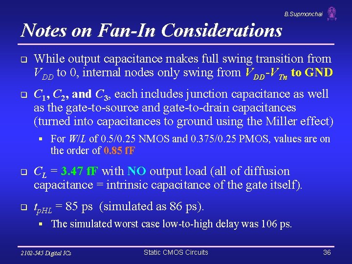
B. Supmonchai Notes on Fan-In Considerations q q While output capacitance makes full swing transition from VDD to 0, internal nodes only swing from VDD-VTn to GND C 1, C 2, and C 3, each includes junction capacitance as well as the gate-to-source and gate-to-drain capacitances (turned into capacitances to ground using the Miller effect) § For W/L of 0. 5/0. 25 NMOS and 0. 375/0. 25 PMOS, values are on the order of 0. 85 f. F q q CL = 3. 47 f. F with NO output load (all of diffusion capacitance = intrinsic capacitance of the gate itself). tp. HL = 85 ps (simulated as 86 ps). § The simulated worst case low-to-high delay was 106 ps. 2102 -545 Digital ICs Static CMOS Circuits 36

B. Supmonchai tp as a Function of Fan-In tp (psec) quadratic tp. HL tp tp. LH linear fan-in Gates with a fan-in greater than 4 should be avoided. 2102 -545 Digital ICs Static CMOS Circuits 37

B. Supmonchai tp as a Function of Fan-Out All gates have the same drive current. tp (psec) tp. NOR 2 tp. NAND 2 tp. INV eff. fan-out Slope is a function of “driving strength” 2102 -545 Digital ICs Static CMOS Circuits 38
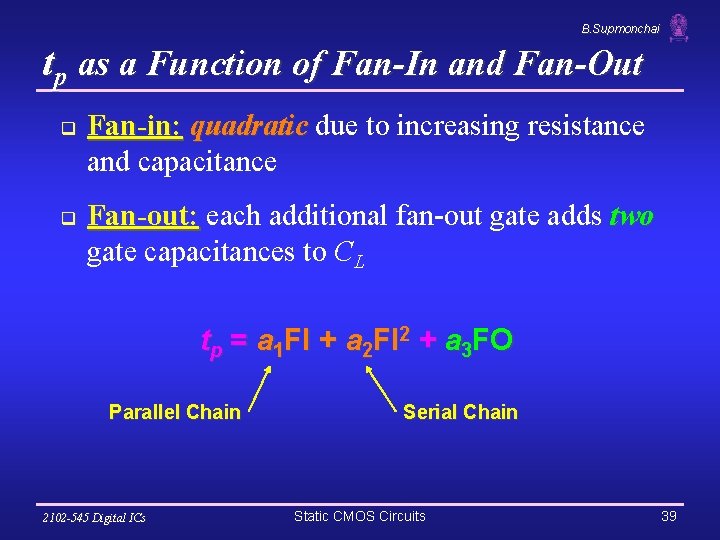
B. Supmonchai tp as a Function of Fan-In and Fan-Out q q Fan-in: quadratic due to increasing resistance and capacitance Fan-out: each additional fan-out gate adds two gate capacitances to CL tp = a 1 FI + a 2 FI 2 + a 3 FO Parallel Chain 2102 -545 Digital ICs Serial Chain Static CMOS Circuits 39
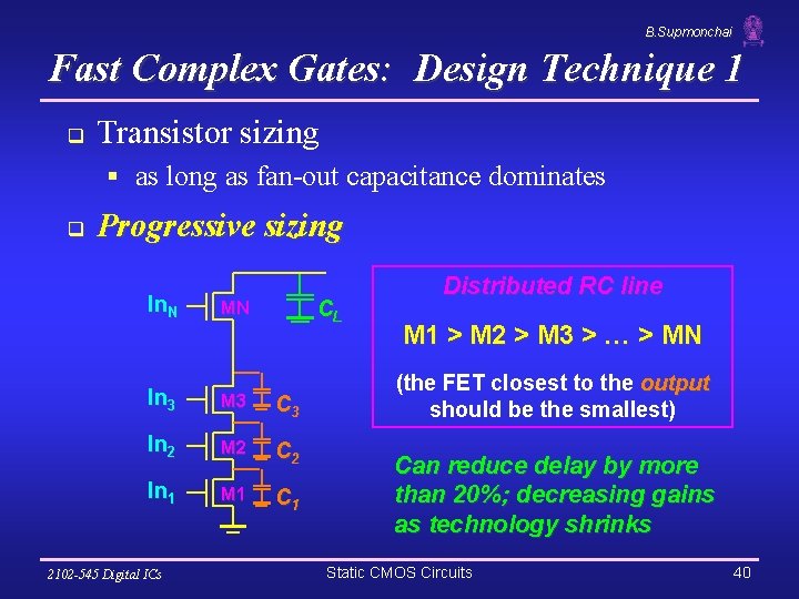
B. Supmonchai Fast Complex Gates: Design Technique 1 q Transistor sizing § as long as fan-out capacitance dominates q Progressive sizing In. N CL MN In 3 M 3 C 3 In 2 M 2 C 2 In 1 M 1 C 1 2102 -545 Digital ICs Distributed RC line M 1 > M 2 > M 3 > … > MN (the FET closest to the output should be the smallest) Can reduce delay by more than 20%; decreasing gains as technology shrinks Static CMOS Circuits 40
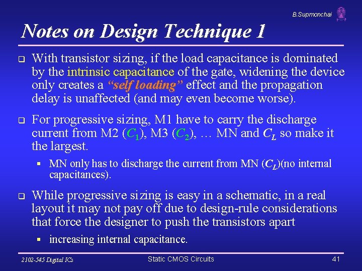
B. Supmonchai Notes on Design Technique 1 q q With transistor sizing, if the load capacitance is dominated by the intrinsic capacitance of the gate, widening the device only creates a “self loading” effect and the propagation delay is unaffected (and may even become worse). For progressive sizing, M 1 have to carry the discharge current from M 2 (C 1), M 3 (C 2), … MN and CL so make it the largest. § MN only has to discharge the current from MN (CL)(no internal capacitances). q While progressive sizing is easy in a schematic, in a real layout it may not pay off due to design-rule considerations that force the designer to push the transistors apart § increasing internal capacitance. 2102 -545 Digital ICs Static CMOS Circuits 41
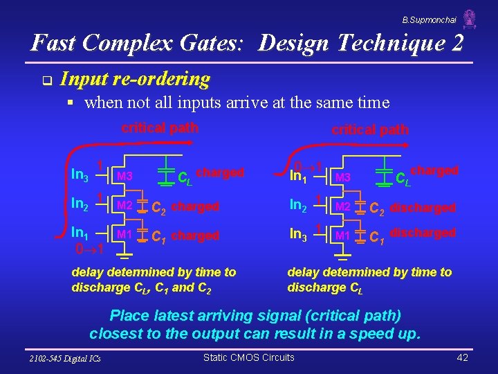
B. Supmonchai Fast Complex Gates: Design Technique 2 q Input re-ordering § when not all inputs arrive at the same time critical path In 3 1 In 2 1 In 1 0 1 M 3 critical path CL charged 0 1 In 1 M 3 charged CL M 2 C 2 charged In 2 1 M 2 C 2 discharged M 1 C 1 charged In 3 1 M 1 C 1 discharged delay determined by time to discharge CL, C 1 and C 2 delay determined by time to discharge CL Place latest arriving signal (critical path) closest to the output can result in a speed up. 2102 -545 Digital ICs Static CMOS Circuits 42
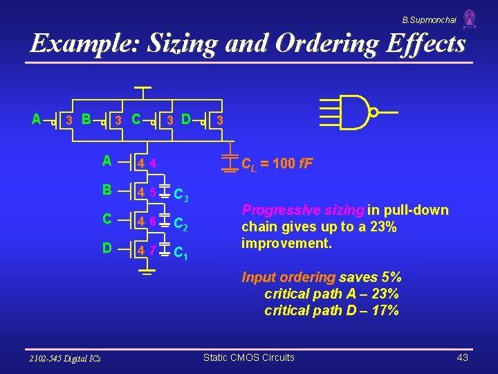
B. Supmonchai Example: Sizing and Ordering Effects A 3 B 3 C A 44 B 45 3 D 3 CL = 100 f. F C 3 C 46 C 2 D 47 C 1 Progressive sizing in pull-down chain gives up to a 23% improvement. Input ordering saves 5% critical path A – 23% critical path D – 17% 2102 -545 Digital ICs Static CMOS Circuits 43
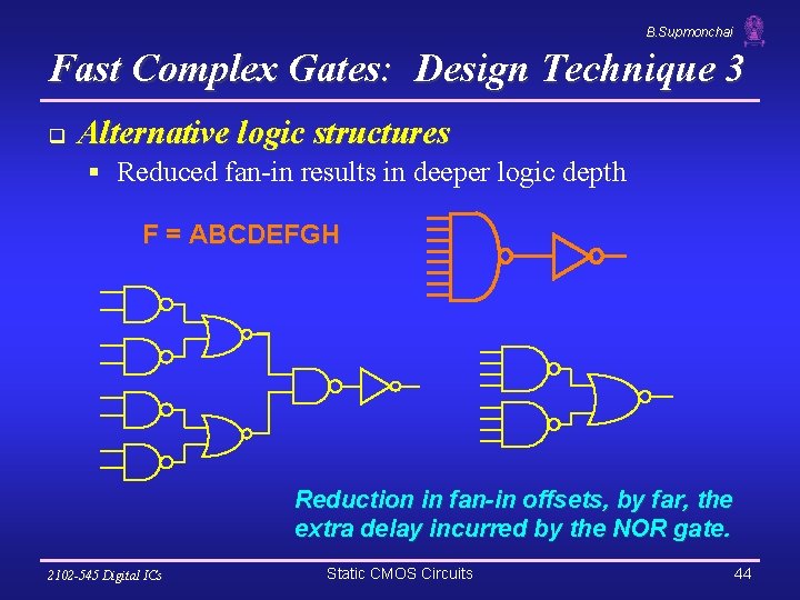
B. Supmonchai Fast Complex Gates: Design Technique 3 q Alternative logic structures § Reduced fan-in results in deeper logic depth F = ABCDEFGH Reduction in fan-in offsets, by far, the extra delay incurred by the NOR gate. 2102 -545 Digital ICs Static CMOS Circuits 44
B. Supmonchai Notes on Design Technique 3 q Reducing fan-in increases logic depth of the circuit § More stages but each stage has smaller delay q Only simulation will tell which of the two alternative configurations is faster and has lower power dissipation. 2102 -545 Digital ICs Static CMOS Circuits 45
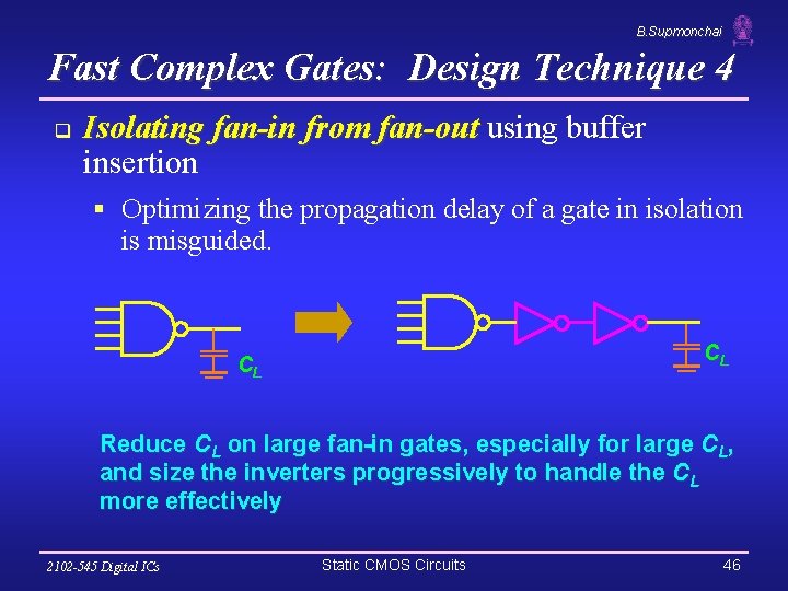
B. Supmonchai Fast Complex Gates: Design Technique 4 q Isolating fan-in from fan-out using buffer insertion § Optimizing the propagation delay of a gate in isolation is misguided. CL CL Reduce CL on large fan-in gates, especially for large CL, and size the inverters progressively to handle the CL more effectively 2102 -545 Digital ICs Static CMOS Circuits 46
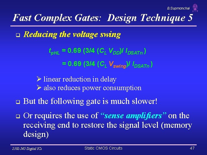
B. Supmonchai Fast Complex Gates: Design Technique 5 q Reducing the voltage swing tp. HL = 0. 69 (3/4 (CL VDD)/ IDSATn ) = 0. 69 (3/4 (CL Vswing)/ IDSATn ) Ø linear reduction in delay Ø also reduces power consumption q q But the following gate is much slower! Or requires the use of “sense amplifiers” on the receiving end to restore the signal level (memory design) 2102 -545 Digital ICs Static CMOS Circuits 47
B. Supmonchai Sizing Logic Paths for Speed q q Frequently, input capacitance of a logic path is constrained Logic also has to drive some capacitance § Example: ALU load in an Intel’s microprocessor is 0. 5 p. F q q How do we size the ALU data path to achieve maximum speed? We have already solved this for the inverter chain – can we generalize it for any type of logic? 2102 -545 Digital ICs Static CMOS Circuits 48
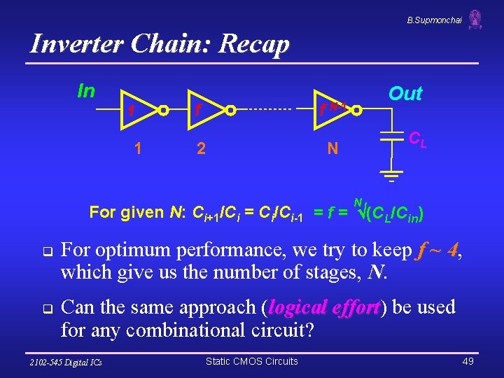
B. Supmonchai Inverter Chain: Recap In 1 1 f f N-1 2 N Out CL N For given N: Ci+1/Ci = Ci/Ci-1 = f = (CL/Cin) q q For optimum performance, we try to keep f ~ 4, 4 which give us the number of stages, N. Can the same approach (logical effort) effort be used for any combinational circuit? 2102 -545 Digital ICs Static CMOS Circuits 49

B. Supmonchai Delay of a Complex Logic Gate q For a complex gate, we expand the inverter chain equation § tp 0 is the intrinsic delay of an inverter § f is the effective fan-out (Cext/Cg) - also called the electrical effort § p is the ratio of the intrinsic (unloaded) delay of the complex gate and a simple inverter (a function of the gate topology and layout style) § g is the logical effort 2102 -545 Digital ICs Static CMOS Circuits 50
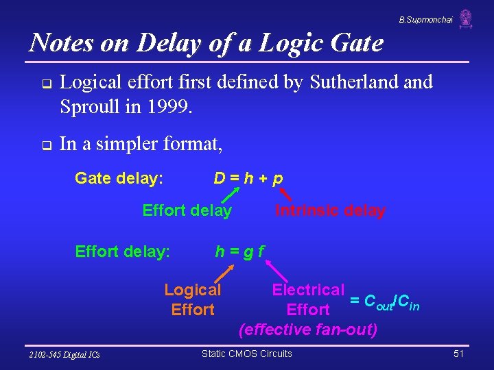
B. Supmonchai Notes on Delay of a Logic Gate q q Logical effort first defined by Sutherland Sproull in 1999. In a simpler format, Gate delay: D=h+p Effort delay: h=gf Logical Effort 2102 -545 Digital ICs Intrinsic delay Electrical = Cout/Cin Effort (effective fan-out) Static CMOS Circuits 51
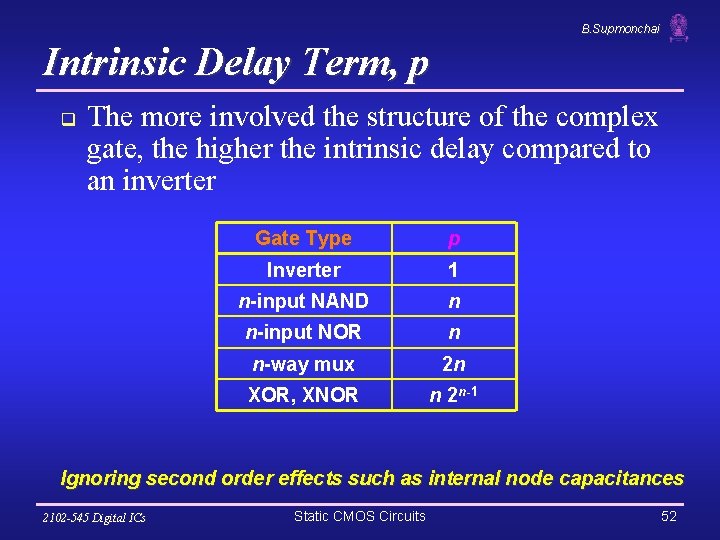
B. Supmonchai Intrinsic Delay Term, p q The more involved the structure of the complex gate, the higher the intrinsic delay compared to an inverter Gate Type p Inverter 1 n-input NAND n n-input NOR n n-way mux 2 n XOR, XNOR n 2 n-1 Ignoring second order effects such as internal node capacitances 2102 -545 Digital ICs Static CMOS Circuits 52
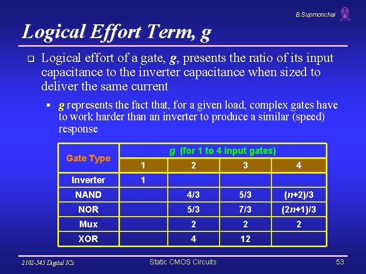
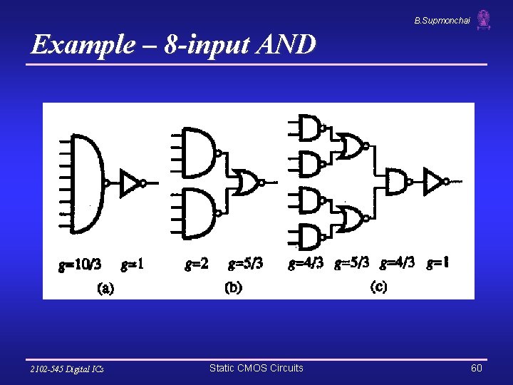
B. Supmonchai Logical Effort Term, g q Logical effort of a gate, g, presents the ratio of its input capacitance to the inverter capacitance when sized to deliver the same current § g represents the fact that, for a given load, complex gates have to work harder than an inverter to produce a similar (speed) response Gate Type 2 3 4 NAND 4/3 5/3 (n+2)/3 NOR 5/3 7/3 (2 n+1)/3 Mux 2 2 2 XOR 4 12 Inverter 2102 -545 Digital ICs g (for 1 to 4 input gates) 1 1 Static CMOS Circuits 53
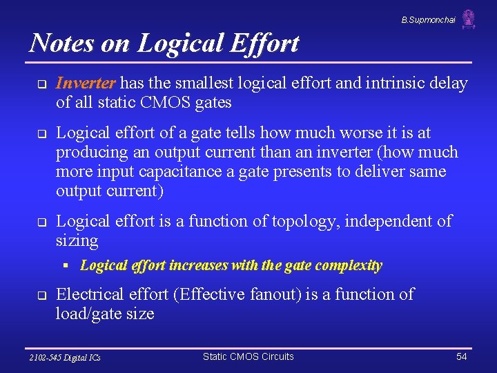
B. Supmonchai Notes on Logical Effort q q q Inverter has the smallest logical effort and intrinsic delay of all static CMOS gates Logical effort of a gate tells how much worse it is at producing an output current than an inverter (how much more input capacitance a gate presents to deliver same output current) Logical effort is a function of topology, independent of sizing § Logical effort increases with the gate complexity q Electrical effort (Effective fanout) is a function of load/gate size 2102 -545 Digital ICs Static CMOS Circuits 54
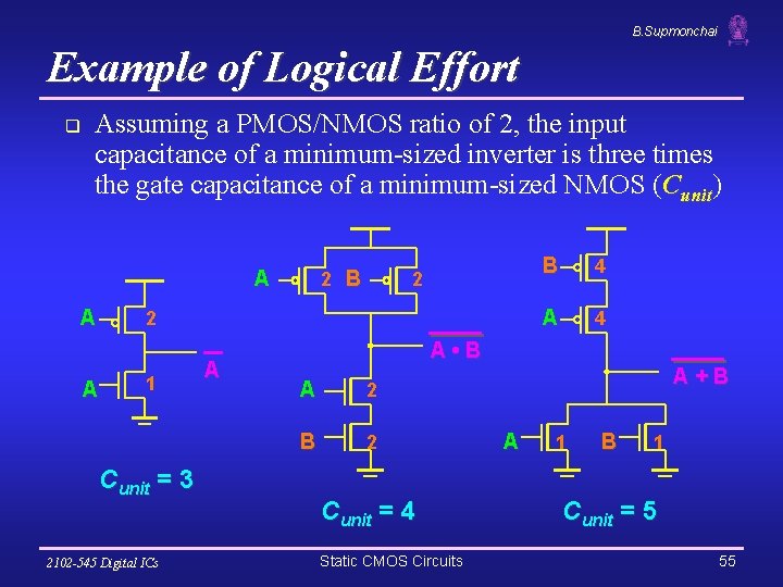
B. Supmonchai Example of Logical Effort q Assuming a PMOS/NMOS ratio of 2, the input capacitance of a minimum-sized inverter is three times the gate capacitance of a minimum-sized NMOS (Cunit) A A 2 B 2 2 A 1 Cunit = 3 2102 -545 Digital ICs A B 4 A • B A 2 B 2 Cunit = 4 Static CMOS Circuits A+B A 1 B 1 Cunit = 5 55

B. Supmonchai Delay as a Function of Fan-Out p , 3 normalized delay / 4 = g : D 2 N A N = 2 q =1 p , =1 g : INV q effort delay q intrinsic delay fan-out f The slope of the line is the logical effort of the gate The y-axis intercept is the intrinsic delay Can adjust the delay by adjusting the effective fan-out (by sizing) or by choosing a gate with a different logical effort Gate Effort: h = fg 2102 -545 Digital ICs Static CMOS Circuits 56
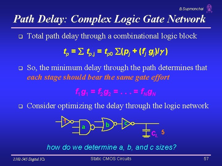
B. Supmonchai Path Delay: Complex Logic Gate Network q Total path delay through a combinational logic block tp = tp, j = tp 0 (pj + (fj gj)/ ) q So, the minimum delay through the path determines that each stage should bear the same gate effort f 1 g 1 = f 2 g 2 =. . . = f. N g N q Consider optimizing the delay through the logic network 1 a b c CL 5 how do we determine a, b, and c sizes? 2102 -545 Digital ICs Static CMOS Circuits 57
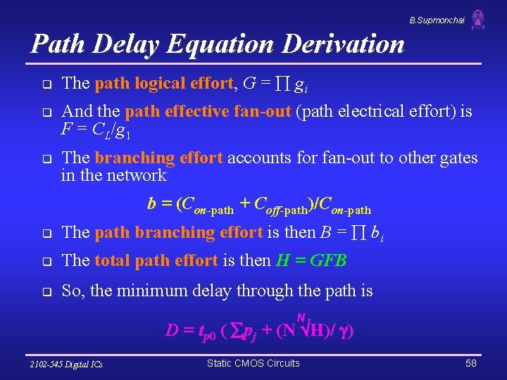
B. Supmonchai Path Delay Equation Derivation q q q The path logical effort, G = gi And the path effective fan-out (path electrical effort) is F = CL/g 1 The branching effort accounts for fan-out to other gates in the network b = (Con-path + Coff-path)/Con-path q The path branching effort is then B = bi q The total path effort is then H = GFB q So, the minimum delay through the path is N D = tp 0 ( pj + (N H)/ ) 2102 -545 Digital ICs Static CMOS Circuits 58

B. Supmonchai Example: Complex Logic Gates q For gate i in the chain, its size is determined by i -1 si = (g 1 s 1)/gi (fj/bj) j=1 q For this network 1 § F = CL/Cg 1 = 5 a b c CL 5 § G = 1 x 5/3 x 1 = 25/9 § B = 1 (no branching) 4 § H = GFB = 125/9, 125/9 so the optimal stage effort is H = 1. 93 Ø Fan-out factors are f 1=1. 93, f 2=1. 93 x 3/5 = 1. 16, f 3 = 1. 16, f 4 = 1. 93 § So the gate sizes are a = f 1 g 1/g 2 = 1. 16, b = f 1 f 2 g 1/g 3 = 1. 34 and c = f 1 f 2 f 3 g 1/g 4 = 2. 60 2102 -545 Digital ICs Static CMOS Circuits 59
B. Supmonchai Example – 8 -input AND 2102 -545 Digital ICs Static CMOS Circuits 60
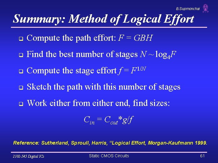
B. Supmonchai Summary: Method of Logical Effort q Compute the path effort: F = GBH q Find the best number of stages N ~ log 4 F q Compute the stage effort f = F 1/N q Sketch the path with this number of stages q Work either from either end, find sizes: Cin = Cout*g/f Reference: Sutherland, Sproull, Harris, “Logical Effort, Morgan-Kaufmann 1999. 2102 -545 Digital ICs Static CMOS Circuits 61
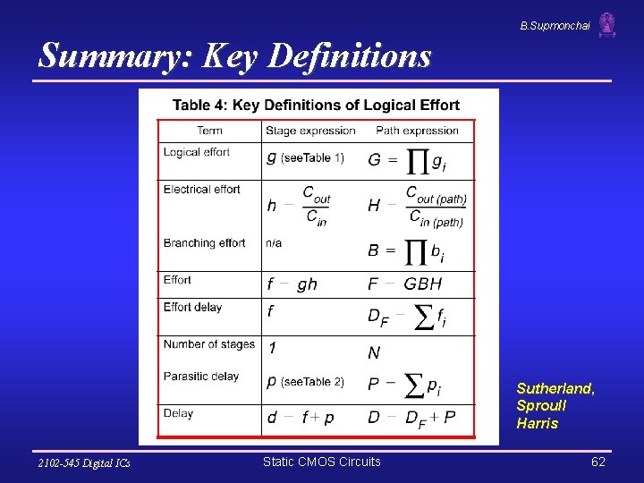
B. Supmonchai Summary: Key Definitions Sutherland, Sproull Harris 2102 -545 Digital ICs Static CMOS Circuits 62
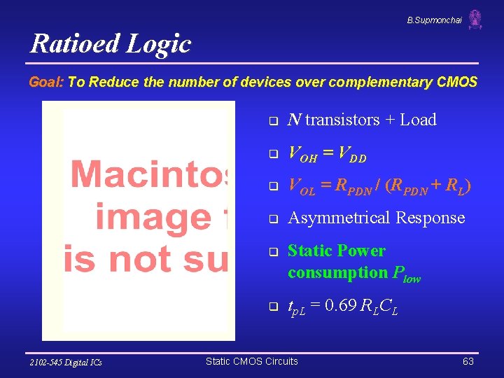
B. Supmonchai Ratioed Logic Goal: To Reduce the number of devices over complementary CMOS q N transistors + Load q VOH = VDD q VOL = RPDN / (RPDN + RL) q Asymmetrical Response q q 2102 -545 Digital ICs Static Power consumption Plow tp. L = 0. 69 RLCL Static CMOS Circuits 63
B. Supmonchai Ratioed Logic: Active Loads 2102 -545 Digital ICs Static CMOS Circuits 64
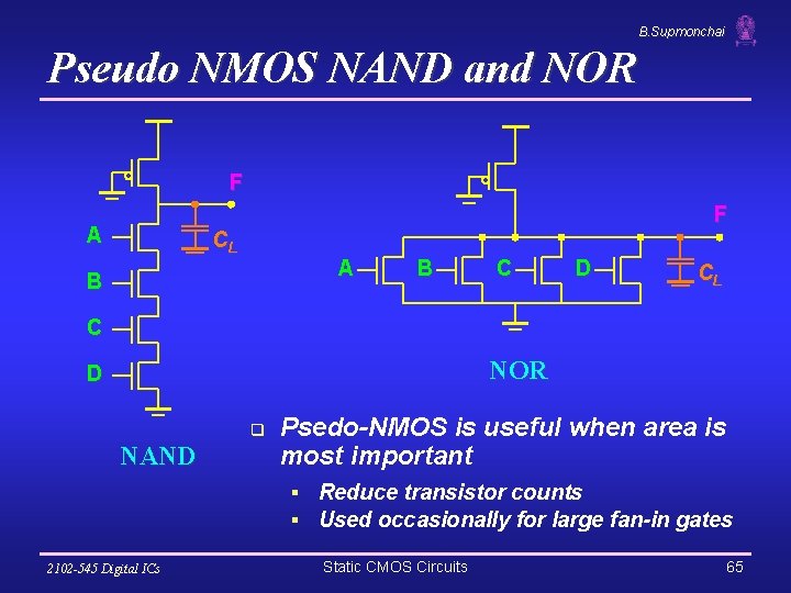
B. Supmonchai Pseudo NMOS NAND and NOR F F A CL A B B C D CL C NOR D q NAND Psedo-NMOS is useful when area is most important § Reduce transistor counts § Used occasionally for large fan-in gates 2102 -545 Digital ICs Static CMOS Circuits 65
B. Supmonchai Pseudo-NMOS Inverter Characteristics q Assumptions: § NMOS resides in linear mode § VOL is small relative to the gate drive (VDD-VT)) 2102 -545 Digital ICs Static CMOS Circuits 66
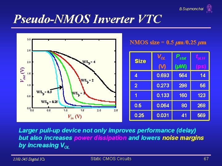
B. Supmonchai Pseudo-NMOS Inverter VTC 3. 0 NMOS size = 0. 5 µm/0. 25 µm 2. 5 Vout (V) Size W/Lp = 4 2. 0 1. 5 W/Lp = 2 1. 0 0. 5 W/Lp = 1 W/Lp = 0. 25 0. 0 0. 5 1. 0 1. 5 2. 0 VOL Pstat tp. LH (V) (µW) (ps) 4 0. 693 564 14 2 0. 273 298 56 1 0. 133 160 123 0. 5 0. 064 80 268 0. 25 0. 031 41 569 2. 5 Vin (V) Larger pull-up device not only improves performance (delay) but also increases power dissipation and lowers noise margins by increasing VOL 2102 -545 Digital ICs Static CMOS Circuits 67
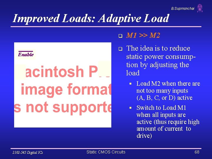
B. Supmonchai Improved Loads: Adaptive Load q Enable q M 1 >> M 2 The idea is to reduce static power consumption by adjusting the load § Load M 2 when there are not too many inputs (A, B, C, or D) active § Switch to Load M 1 when all inputs are active (thus require high amount of current to drive) 2102 -545 Digital ICs Static CMOS Circuits 68
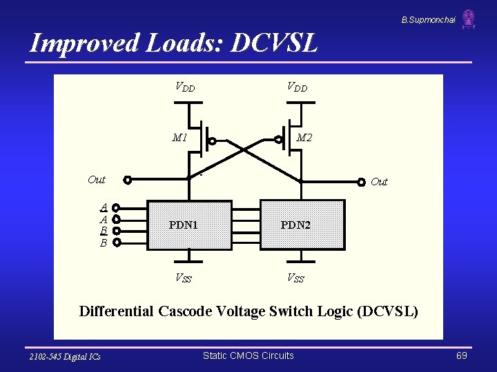
B. Supmonchai Improved Loads: DCVSL VDD M 1 M 2 Out A A B B Out PDN 1 PDN 2 VSS Differential Cascode Voltage Switch Logic (DCVSL) 2102 -545 Digital ICs Static CMOS Circuits 69

B. Supmonchai DCVSL Example 2102 -545 Digital ICs Static CMOS Circuits 70
B. Supmonchai DCVSL Characteristics q Dual Rail Logic § Each input is provided in complementary format and each gate produces complementary output § Increasing complexity q Rail-to-Rail Swing q No static power dissipation q Sizing of the PMOS relative to PDN is critical to functionality, not just performance § PDNs must be strong enough to bring outputs below VDD - |VTp| 2102 -545 Digital ICs Static CMOS Circuits 71
![B. Supmonchai DCVSL Transient Response V olta ge [V] 2. 5 tin->out = 197 B. Supmonchai DCVSL Transient Response V olta ge [V] 2. 5 tin->out = 197](http://slidetodoc.com/presentation_image_h/f9b7e93ff4a08cc313f27beec4073d98/image-72.jpg)
B. Supmonchai DCVSL Transient Response V olta ge [V] 2. 5 tin->out = 197 ps AB 1. 5 0. 5 -0. 5 0 AB A, B 0. 2 tin->out = 321 ps A, B 0. 4 0. 6 Time [ns] 0. 8 1. 0 Transient Response of a 2 -input AND/NAND gate. How does it look like? 2102 -545 Digital ICs Static CMOS Circuits 72
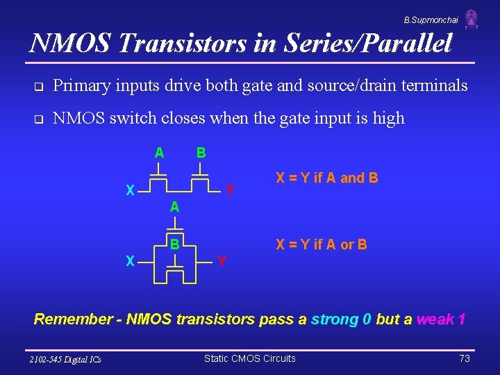
B. Supmonchai NMOS Transistors in Series/Parallel q Primary inputs drive both gate and source/drain terminals q NMOS switch closes when the gate input is high A B X Y X = Y if A and B A B X X = Y if A or B Y Remember - NMOS transistors pass a strong 0 but a weak 1 2102 -545 Digital ICs Static CMOS Circuits 73
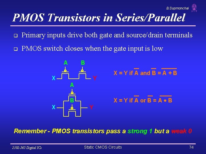
B. Supmonchai PMOS Transistors in Series/Parallel q Primary inputs drive both gate and source/drain terminals q PMOS switch closes when the gate input is low A B X Y X = Y if A and B = A + B A X = Y if A or B = A B B X Y Remember - PMOS transistors pass a strong 1 but a weak 0 2102 -545 Digital ICs Static CMOS Circuits 74
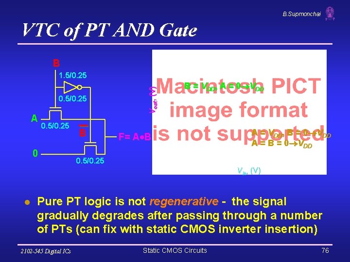
B. Supmonchai VTC of PT AND Gate B 0. 5/0. 25 A 0. 5/0. 25 0 B Vout, (V) 1. 5/0. 25 B = VDD, A = 0 VDD F= A B A = VDD, B = 0 VDD A = B = 0 VDD 0. 5/0. 25 Vin, (V) l Pure PT logic is not regenerative - the signal gradually degrades after passing through a number of PTs (can fix with static CMOS inverter insertion) 2102 -545 Digital ICs Static CMOS Circuits 76
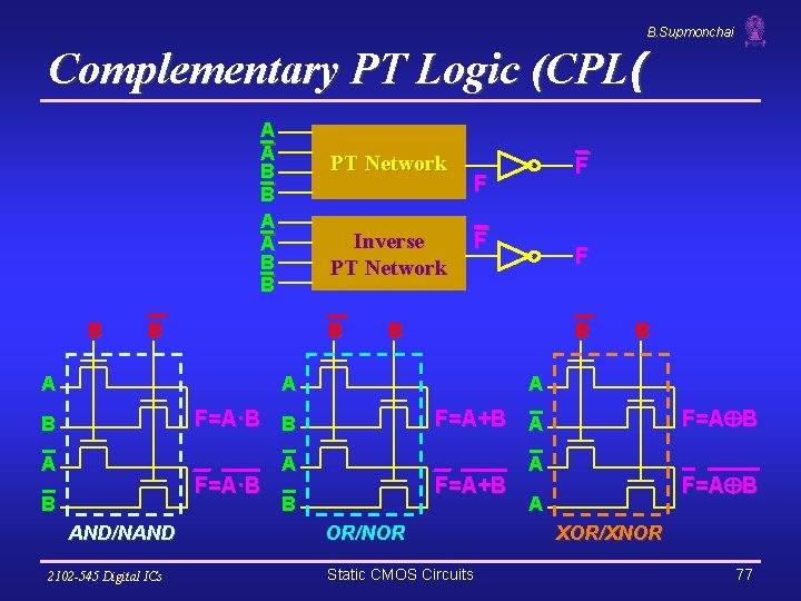
B. Supmonchai Complementary PT Logic (CPL( A A B B B PT Network Inverse PT Network B B F F B B A A A B F=A·B B F=A+B A A F=A·B B AND/NAND 2102 -545 Digital ICs F=A+B B OR/NOR Static CMOS Circuits B F=A B A XOR/XNOR 77
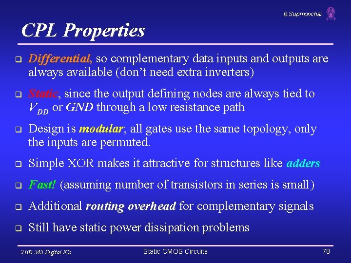
B. Supmonchai CPL Properties q q q Differential, so complementary data inputs and outputs are always available (don’t need extra inverters) Static, Static since the output defining nodes are always tied to VDD or GND through a low resistance path Design is modular; modular all gates use the same topology, only the inputs are permuted. q Simple XOR makes it attractive for structures like adders q Fast! (assuming number of transistors in series is small) q Additional routing overhead for complementary signals q Still have static power dissipation problems 2102 -545 Digital ICs Static CMOS Circuits 78
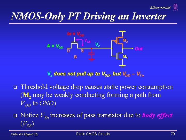
B. Supmonchai NMOS-Only PT Driving an Inverter In = VDD A = VDD VGS D Vx M 2 Out S B M 1 Vx does not pull up to VDD, but VDD – VTn q q Threshold voltage drop causes static power consumption (M 2 may be weakly conducting forming a path from VDD to GND) Notice VTn increases of pass transistor due to body effect (VSB) 2102 -545 Digital ICs Static CMOS Circuits 79
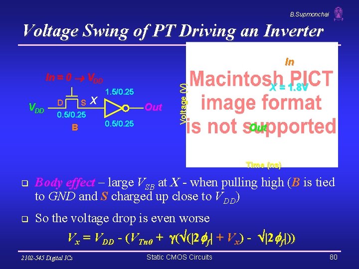
B. Supmonchai Voltage Swing of PT Driving an Inverter In = 0 VDD S VDD D 0. 5/0. 25 B X 1. 5/0. 25 Out 0. 5/0. 25 Voltage (V) In X = 1. 8 V Out Time (ns) q q Body effect – large VSB at X - when pulling high (B is tied to GND and S charged up close to VDD) So the voltage drop is even worse Vx = VDD - (VTn 0 + ( (|2 f| + Vx) - |2 f|)) 2102 -545 Digital ICs Static CMOS Circuits 80
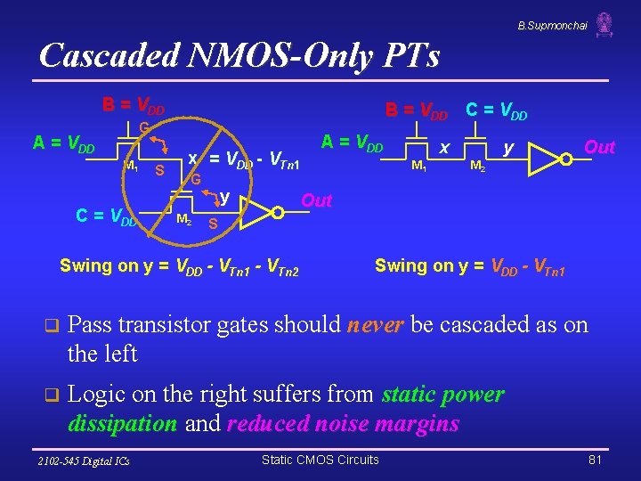
B. Supmonchai Cascaded NMOS-Only PTs B = VDD C = VDD G A = VDD M 1 C = VDD S x = VDD - VTn 1 G M 2 y A = VDD x M 1 y Out M 2 Out S Swing on y = VDD - VTn 1 - VTn 2 Swing on y = VDD - VTn 1 q Pass transistor gates should never be cascaded as on the left q Logic on the right suffers from static power dissipation and reduced noise margins 2102 -545 Digital ICs Static CMOS Circuits 81
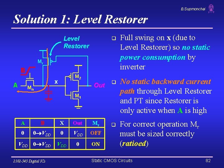
B. Supmonchai Solution 1: Level Restorer q Mr B A M 2 x Mn Out q q M 1 A B X Out Mr 0 0 VDD OFF VDD 0 ON 2102 -545 Digital ICs Full swing on x (due to Level Restorer) so no static power consumption by inverter No static backward current path through Level Restorer and PT since Restorer is only active when A is high For correct operation Mr must be sized correctly (ratioed) ratioed Static CMOS Circuits 82

B. Supmonchai Transient Level Restorer Circuit Response Voltage (V) W/Ln=0. 50/0. 25, W/L 1=0. 50/0. 25, W/L 2=1. 50/0. 25 W/Lr=1. 75/0. 25 node x never goes below VM of inverter so output never switches W/Lr=1. 50/0. 25 W/Lr=1. 25/0. 25 Time (ps) q Restorer has speed and power impacts: § Increases the capacitance at x, slowing down the gate § Increases tr (but decreases tf) 2102 -545 Digital ICs Static CMOS Circuits 83
B. Supmonchai Notes on Level Restorer q q Pull down must be stronger than restorer (pull up) to switch node X If resistance of restorer transistor is too small (too wide transistor) it is impossible to bring the voltage at node X below the switching threshold of the inverter, and the inverter never switches! Sizing of Mr is critical for DC functionality, not just performance!! It belongs to Dynamic Logic Family 2102 -545 Digital ICs Static CMOS Circuits 84
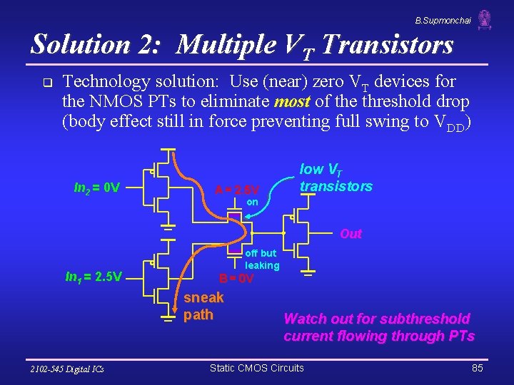
B. Supmonchai Solution 2: Multiple VT Transistors q Technology solution: Use (near) zero VT devices for the NMOS PTs to eliminate most of the threshold drop (body effect still in force preventing full swing to VDD) In 2 = 0 V A = 2. 5 V low VT transistors on Out In 1 = 2. 5 V off but leaking B = 0 V sneak path 2102 -545 Digital ICs Watch out for subthreshold current flowing through PTs Static CMOS Circuits 85
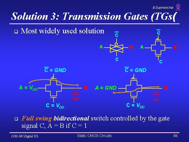
B. Supmonchai Solution 3: Transmission Gates (TGs( q Most widely used solution C C A B A C C = GND A = VDD C C = GND B A = GND B C = VDD q B Full swing bidirectional switch controlled by the gate signal C, A = B if C = 1 2102 -545 Digital ICs Static CMOS Circuits 86

B. Supmonchai Resistance of TG W/Lp=0. 50/0. 25 0 V Resistance (k ) Rn Rp Req = Rp || Rn Rp 2. 5 V Vout Rn Req 2. 5 V W/Ln=0. 50/0. 25 Vout (V) q q TG is not an ideal switch - series resistance Req is relatively constant ( about 8 kohms in this case), so can assume has a constant resistance 2102 -545 Digital ICs Static CMOS Circuits 87
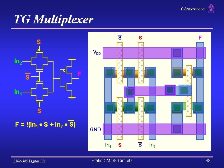
B. Supmonchai TG Multiplexer S S S F VDD In 2 F S In 1 S F = !(In 1 S + In 2 S) GND In 1 2102 -545 Digital ICs Static CMOS Circuits In 2 88
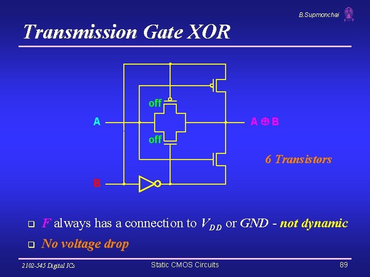
B. Supmonchai Transmission Gate XOR off A B A off 6 Transistors B q F always has a connection to VDD or GND - not dynamic q No voltage drop 2102 -545 Digital ICs Static CMOS Circuits 89
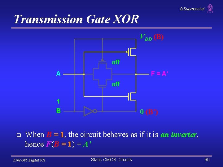
B. Supmonchai Transmission Gate XOR VDD (B) off A F = A‘ off 1 B q 0 (B’) When B = 1, 1 the circuit behaves as if it is an inverter, inverter hence F(B = 1) 1 = A’ 2102 -545 Digital ICs Static CMOS Circuits 90
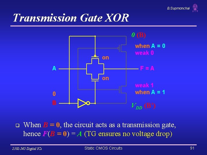
B. Supmonchai Transmission Gate XOR 0 (B) on A when A = 0 weak 0 F=A on weak 1 when A = 1 0 B q VDD (B’) When B = 0, 0 the circuit acts as a transmission gate, hence F(B = 0) 0 = A (TG ensures no voltage drop) 2102 -545 Digital ICs Static CMOS Circuits 91
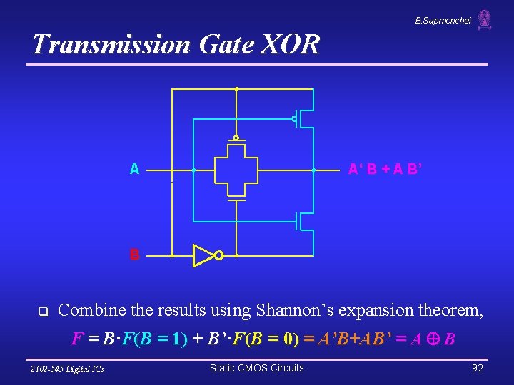
B. Supmonchai Transmission Gate XOR A A‘ B + A B’ B q Combine the results using Shannon’s expansion theorem, F = B·F(B = 1) + B’·F(B = 0) = A’B+AB’ = A B 2102 -545 Digital ICs Static CMOS Circuits 92
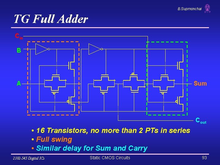
B. Supmonchai TG Full Adder Cin B A Sum Cout • 16 Transistors, no more than 2 PTs in series • Full swing • Similar delay for Sum and Carry 2102 -545 Digital ICs Static CMOS Circuits 93

B. Supmonchai Delay of a TG Chain 0 0 Vin V 1 5 C Vin Req C q 0 Vi 5 C V 1 0 Req C Vi+1 5 C Vi Req VN 5 C Vi+1 C Req VN C Delay of the RC chain (N TG’s in series) is tp(Vn) = 0. 69 k. CReq = 0. 69 CReq (N(N+1))/2 0. 35 CReq. N 2 2102 -545 Digital ICs Static CMOS Circuits 95
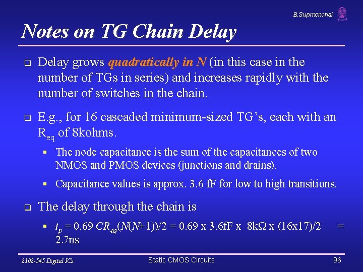
B. Supmonchai Notes on TG Chain Delay q q Delay grows quadratically in N (in this case in the number of TGs in series) and increases rapidly with the number of switches in the chain. E. g. , for 16 cascaded minimum-sized TG’s, each with an Req of 8 kohms. § The node capacitance is the sum of the capacitances of two NMOS and PMOS devices (junctions and drains). § Capacitance values is approx. 3. 6 f. F for low to high transitions. q The delay through the chain is § tp = 0. 69 CReq(N(N+1))/2 = 0. 69 x 3. 6 f. F x 8 kΩ x (16 x 17)/2 = 2. 7 ns 2102 -545 Digital ICs Static CMOS Circuits 96
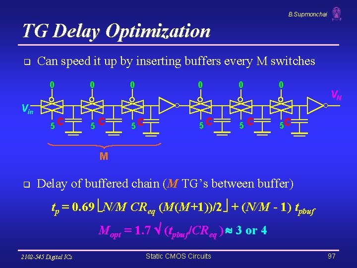
B. Supmonchai TG Delay Optimization q Can speed it up by inserting buffers every M switches 0 0 0 5 C 5 C 5 C VN Vin M q Delay of buffered chain (M TG’s between buffer) tp = 0. 69 N/M CReq (M(M+1))/2 + (N/M - 1) tpbuf Mopt = 1. 7 (tpbuf/CReq ) 3 or 4 2102 -545 Digital ICs Static CMOS Circuits 97
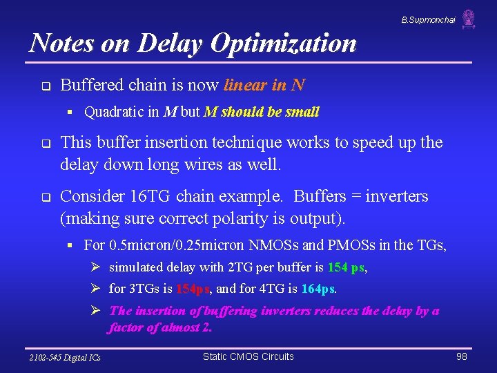
B. Supmonchai Notes on Delay Optimization q Buffered chain is now linear in N § Quadratic in M but M should be small q q This buffer insertion technique works to speed up the delay down long wires as well. Consider 16 TG chain example. Buffers = inverters (making sure correct polarity is output). § For 0. 5 micron/0. 25 micron NMOSs and PMOSs in the TGs, Ø simulated delay with 2 TG per buffer is 154 ps, ps Ø for 3 TGs is 154 ps, 154 ps and for 4 TG is 164 ps Ø The insertion of buffering inverters reduces the delay by a factor of almost 2. 2102 -545 Digital ICs Static CMOS Circuits 98
- Slides: 96