Chapter 6 MOSFET The MOSFET MOS FieldEffect Transistor
- Slides: 29

Chapter 6 MOSFET The MOSFET (MOS Field-Effect Transistor) is the building block of Gb memory chips, GHz microprocessors, analog, and RF circuits. Match the following MOSFET characteristics with their applications: • small size • high speed • low power • high gain Modern Semiconductor Devices for Integrated Circuits (C. Hu) Slide 6 -1

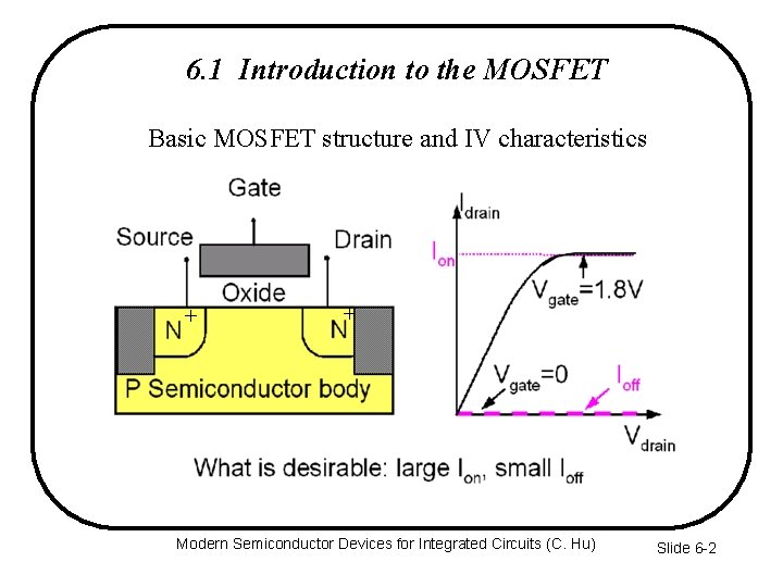
6. 1 Introduction to the MOSFET Basic MOSFET structure and IV characteristics + + Modern Semiconductor Devices for Integrated Circuits (C. Hu) Slide 6 -2

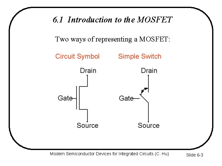
6. 1 Introduction to the MOSFET Two ways of representing a MOSFET: Modern Semiconductor Devices for Integrated Circuits (C. Hu) Slide 6 -3

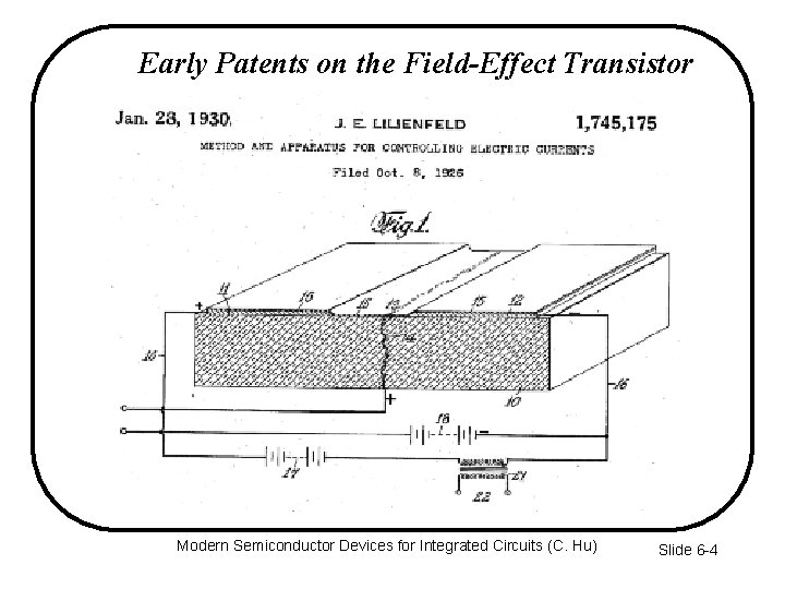
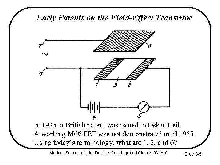
Early Patents on the Field-Effect Transistor Modern Semiconductor Devices for Integrated Circuits (C. Hu) Slide 6 -4

Early Patents on the Field-Effect Transistor In 1935, a British patent was issued to Oskar Heil. A working MOSFET was not demonstrated until 1955. Using today’s terminology, what are 1, 2, and 6? Modern Semiconductor Devices for Integrated Circuits (C. Hu) Slide 6 -5

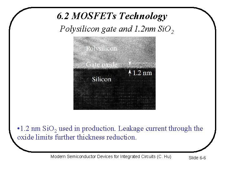
6. 2 MOSFETs Technology Polysilicon gate and 1. 2 nm Si. O 2 • 1. 2 nm Si. O 2 used in production. Leakage current through the oxide limits further thickness reduction. Modern Semiconductor Devices for Integrated Circuits (C. Hu) Slide 6 -6

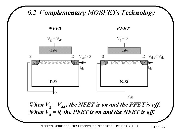
6. 2 Complementary MOSFETs Technology NFET PFET When Vg = Vdd , the NFET is on and the PFET is off. When Vg = 0, the PFET is on and the NFET is off. Modern Semiconductor Devices for Integrated Circuits (C. Hu) Slide 6 -7

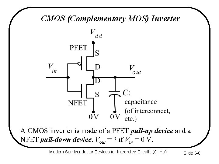
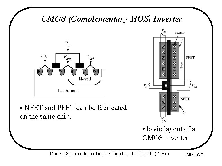
CMOS (Complementary MOS) Inverter A CMOS inverter is made of a PFET pull-up device and a NFET pull-down device. Vout = ? if Vin = 0 V. Modern Semiconductor Devices for Integrated Circuits (C. Hu) Slide 6 -8

CMOS (Complementary MOS) Inverter • NFET and PFET can be fabricated on the same chip. • basic layout of a CMOS inverter Modern Semiconductor Devices for Integrated Circuits (C. Hu) Slide 6 -9

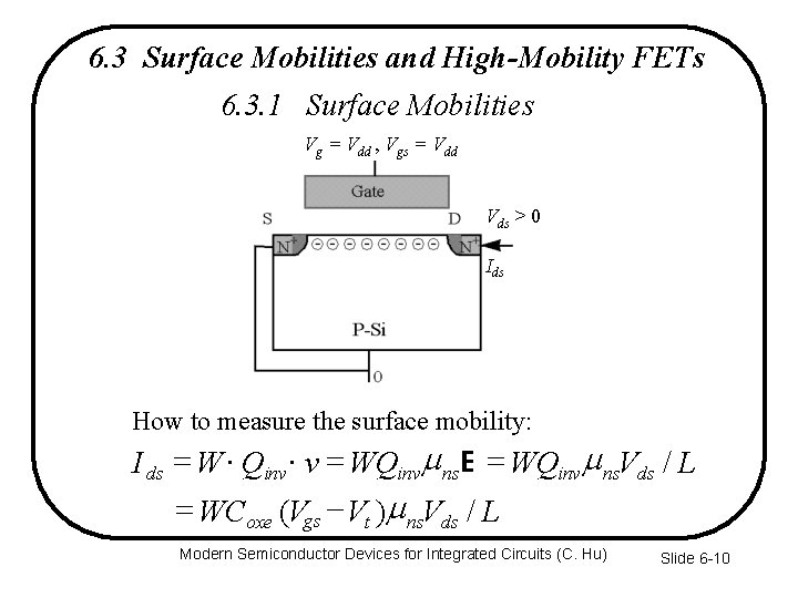
6. 3 Surface Mobilities and High-Mobility FETs 6. 3. 1 Surface Mobilities Vg = Vdd , Vgs = Vdd Vds > 0 Ids How to measure the surface mobility: I ds = W × Qinv × v = WQinv ns. E = WQinv ns. Vds / L = WCoxe (Vgs - Vt ) ns. Vds / L Modern Semiconductor Devices for Integrated Circuits (C. Hu) Slide 6 -10

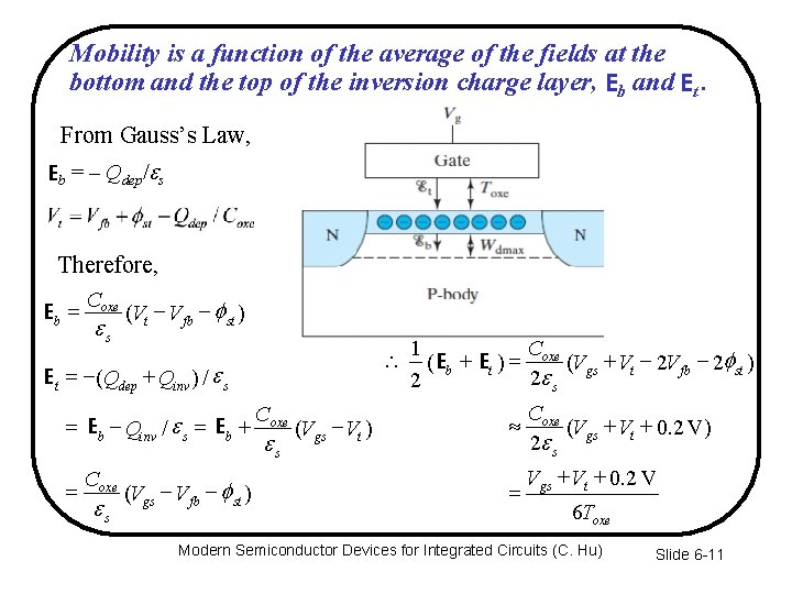
Mobility is a function of the average of the fields at the bottom and the top of the inversion charge layer, Eb and Et. From Gauss’s Law, Eb = – Qdep/es Therefore, Eb = Coxe es (Vt - V fb - f st ) E t = -(Qdep + Qinv ) / e s = Eb - Qinv / e s = Eb + = Coxe es (Vgs - V fb - f st ) Coxe es (Vgs - Vt ) Coxe 1 E + = E ( b (Vgs + Vt - 2 V fb - 2 f st ) t) 2 e s 2 » = Coxe (Vgs + Vt + 0. 2 V) 2 e s Vgs + Vt + 0. 2 V 6 Toxe Modern Semiconductor Devices for Integrated Circuits (C. Hu) Slide 6 -11

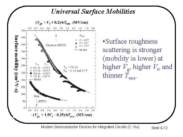
Universal Surface Mobilities Surface mobility (cm 2/V-s) • Surface roughness scattering is stronger (mobility is lower) at higher Vg, higher Vt, and thinner Toxe. Modern Semiconductor Devices for Integrated Circuits (C. Hu) Slide 6 -12

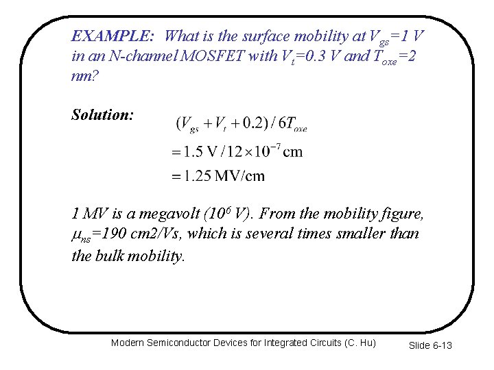
EXAMPLE: What is the surface mobility at Vgs=1 V in an N-channel MOSFET with Vt=0. 3 V and Toxe=2 nm? Solution: 1 MV is a megavolt (106 V). From the mobility figure, ns=190 cm 2/Vs, which is several times smaller than the bulk mobility. Modern Semiconductor Devices for Integrated Circuits (C. Hu) Slide 6 -13

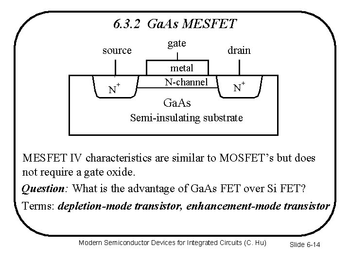
6. 3. 2 Ga. As MESFET source N + gate metal N-channel drain N + Ga. As Semi-insulating substrate MESFET IV characteristics are similar to MOSFET’s but does not require a gate oxide. Question: What is the advantage of Ga. As FET over Si FET? Terms: depletion-mode transistor, enhancement-mode transistor Modern Semiconductor Devices for Integrated Circuits (C. Hu) Slide 6 -14

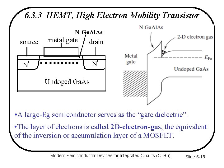
6. 3. 3 HEMT, High Electron Mobility Transistor N-Ga. Al. As source + N metal gate drain …. . . . + N Undoped Ga. As • A large-Eg semiconductor serves as the “gate dielectric”. • The layer of electrons is called 2 D-electron-gas, the equivalent of the inversion or accumulation layer of a MOSFET. Modern Semiconductor Devices for Integrated Circuits (C. Hu) Slide 6 -15

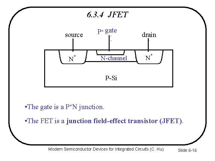
6. 3. 4 JFET source N + P+ gate N-channel drain N + P-Si • The gate is a P+N junction. • The FET is a junction field-effect transistor (JFET). Modern Semiconductor Devices for Integrated Circuits (C. Hu) Slide 6 -16

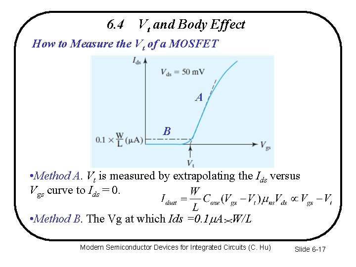
6. 4 Vt and Body Effect How to Measure the Vt of a MOSFET A B • Method A. Vt is measured by extrapolating the Ids versus Vgs curve to Ids = 0. • Method B. The Vg at which Ids =0. 1 A W/L Modern Semiconductor Devices for Integrated Circuits (C. Hu) Slide 6 -17

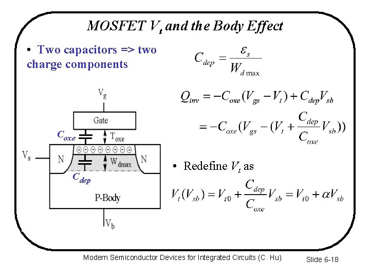
MOSFET Vt and the Body Effect • Two capacitors => two charge components Coxe Cdep • Redefine Vt as Modern Semiconductor Devices for Integrated Circuits (C. Hu) Slide 6 -18

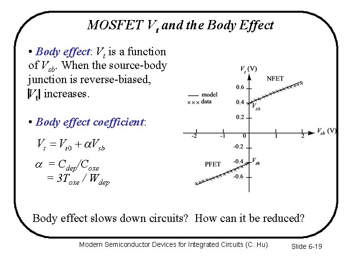
MOSFET Vt and the Body Effect • Body effect: Vt is a function of Vsb. When the source-body junction is reverse-biased, Vt increases. • Body effect coefficient: a = Cdep/Coxe = 3 Toxe / Wdep Body effect slows down circuits? How can it be reduced? Modern Semiconductor Devices for Integrated Circuits (C. Hu) Slide 6 -19

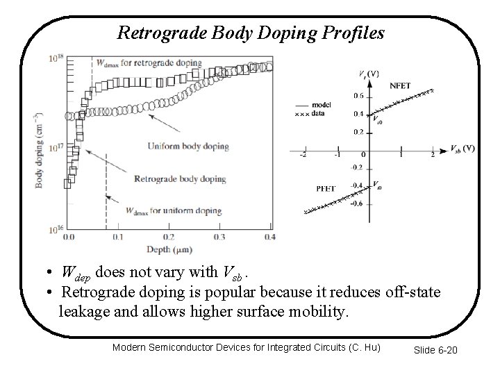
Retrograde Body Doping Profiles Wdmax for retrograde doping Wdmax for uniform doping • Wdep does not vary with Vsb. • Retrograde doping is popular because it reduces off-state leakage and allows higher surface mobility. Modern Semiconductor Devices for Integrated Circuits (C. Hu) Slide 6 -20

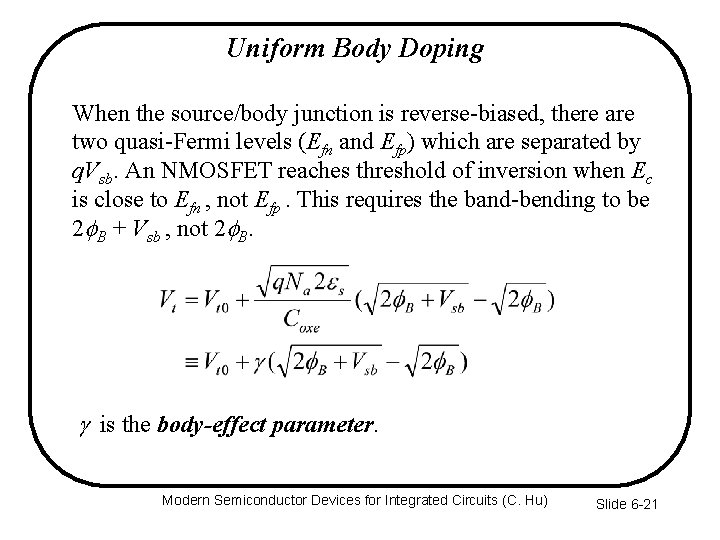
Uniform Body Doping When the source/body junction is reverse-biased, there are two quasi-Fermi levels (Efn and Efp) which are separated by q. Vsb. An NMOSFET reaches threshold of inversion when Ec is close to Efn , not Efp. This requires the band-bending to be 2 f. B + Vsb , not 2 f. B. g is the body-effect parameter. Modern Semiconductor Devices for Integrated Circuits (C. Hu) Slide 6 -21

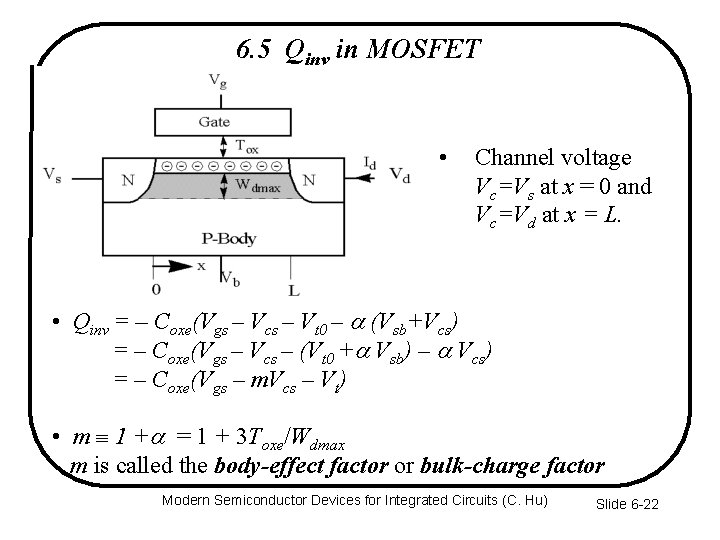
6. 5 Qinv in MOSFET • Channel voltage Vc=Vs at x = 0 and Vc=Vd at x = L. • Qinv = – Coxe(Vgs – Vcs – Vt 0 – a (Vsb+Vcs) = – Coxe(Vgs – Vcs – (Vt 0 +a Vsb) – a Vcs) = – Coxe(Vgs – m. Vcs – Vt) • m º 1 +a = 1 + 3 Toxe/Wdmax m is called the body-effect factor or bulk-charge factor Modern Semiconductor Devices for Integrated Circuits (C. Hu) Slide 6 -22

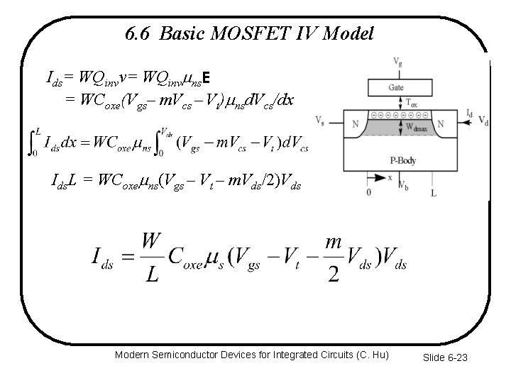
6. 6 Basic MOSFET IV Model Ids= WQinvv= WQinv ns. E = WCoxe(Vgs– m. Vcs – Vt) nsd. Vcs/dx Ids. L = WCoxe ns(Vgs – Vt – m. Vds/2)Vds Modern Semiconductor Devices for Integrated Circuits (C. Hu) Slide 6 -23

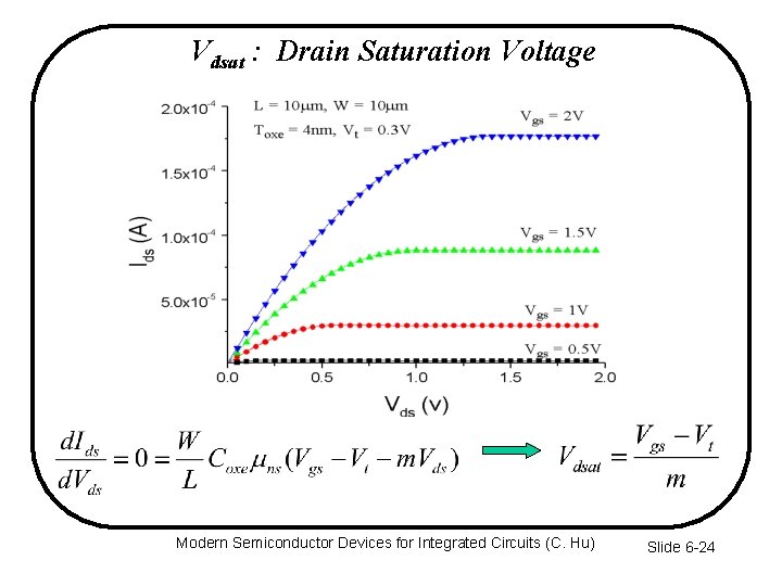
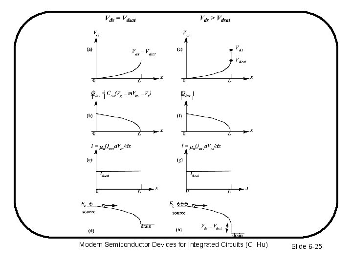
Vdsat : Drain Saturation Voltage Modern Semiconductor Devices for Integrated Circuits (C. Hu) Slide 6 -24

Modern Semiconductor Devices for Integrated Circuits (C. Hu) Slide 6 -25

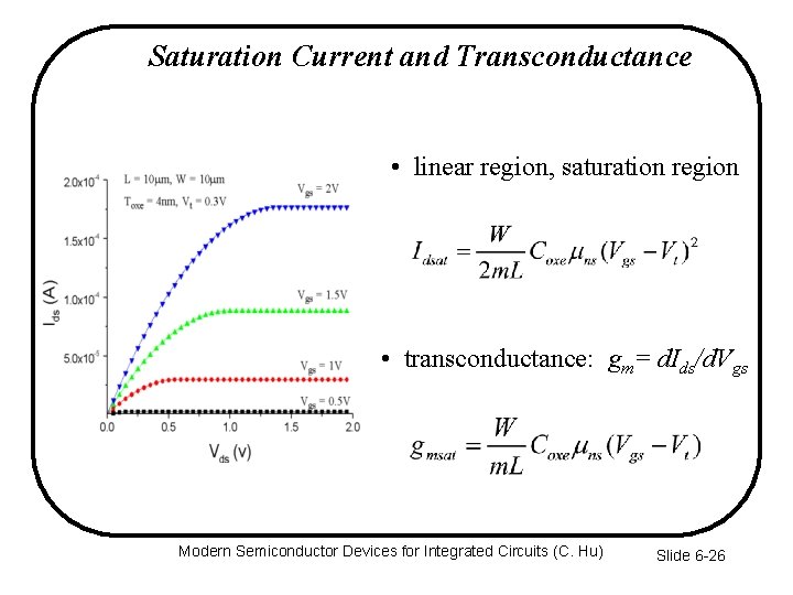
Saturation Current and Transconductance • linear region, saturation region • transconductance: gm= d. Ids/d. Vgs Modern Semiconductor Devices for Integrated Circuits (C. Hu) Slide 6 -26

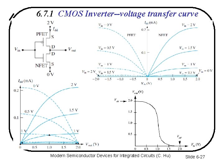
6. 7. 1 CMOS Inverter--voltage transfer curve Modern Semiconductor Devices for Integrated Circuits (C. Hu) Slide 6 -27

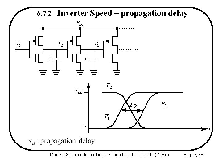
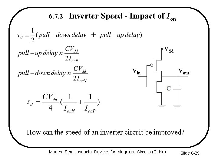
6. 7. 2 Inverter Speed – propagation delay Vdd V 1 . . . V 2 V 3 C . . . C V 2 Vdd 2 td V 3 V 1 0 Modern Semiconductor Devices for Integrated Circuits (C. Hu) t Slide 6 -28

6. 7. 2 Inverter Speed - Impact of Ion Vdd Vin Vout How can the speed of an inverter circuit be improved? Modern Semiconductor Devices for Integrated Circuits (C. Hu) Slide 6 -29