CHAPTER 6 Field Effect Transistors FETs Miss Mardianaliza




- Slides: 23

CHAPTER 6 Field Effect Transistors (FETs) Miss Mardianaliza Bt Othman PPKSE

Objectives Ø Explain the operation and characteristics of junction field effect transistors (JFET). Ø Understand JFET parameters Ø Explain the operation and characteristics of metal oxide semiconductor field effect transistors (MOSFET) Ø Discuss and analyze how MOSFET are biased Ø Troubleshoot FET circuits.

Introduction • FET – a three-terminal voltage-controlled device used in amplification and switching application. • Field effect transistors controls current by voltage applied to the gate. The FET’s major advantage over the BJT is high input resistance. • 2 basic type of FET: JFET and MOSFET

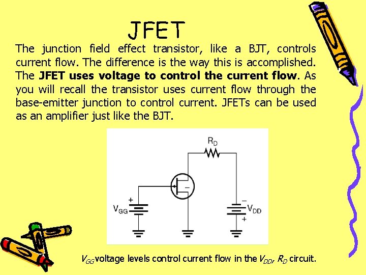
JFET The junction field effect transistor, like a BJT, controls current flow. The difference is the way this is accomplished. The JFET uses voltage to control the current flow. As you will recall the transistor uses current flow through the base-emitter junction to control current. JFETs can be used as an amplifier just like the BJT. VGG voltage levels control current flow in the. VDD, RD circuit.

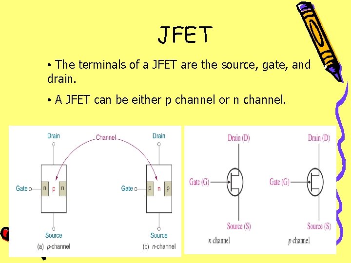
JFET • The terminals of a JFET are the source, gate, and drain. • A JFET can be either p channel or n channel.

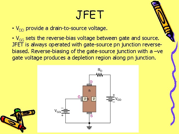
JFET • VDD provide a drain-to-source voltage. • VGG sets the reverse-bias voltage between gate and source. JFET is always operated with gate-source pn junction reversebiased. Reverse-biasing of the gate-source junction with a –ve gate voltage produces a depletion region along pn junction.

JFET Input Resistance Since JFET is reverse-biased for operation, its input resistance becomes so large. This is an advantage of using JFET. Looking at the datasheet, you may calculate the resistance value by using the Gate Reverse Current IGSS. This internal input resistance can be calculated at different VGS : RIN=|VGS/IGSS| As IGSS increases with temperature, RIN will decrease.

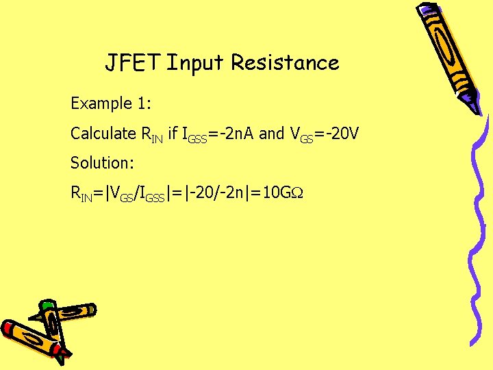
JFET Input Resistance Example 1: Calculate RIN if IGSS=-2 n. A and VGS=-20 V Solution: RIN=|VGS/IGSS|=|-20/-2 n|=10 G

JFET Biasing – gate-bias • Gate supply voltage (-VGG) is used to ensure gate-tosource junction is reverse-biased. Since there is no gate current, there is no voltage dropped across RG. So, VGS = -VGG. • RG to prevent input signal from being shorted to gate supply through low reactance of input coupling capacitor. • To find ID, use ID = IDSS(1 - VGS/VGS(off))2 • VDS= VDD – IDRD • Diadvantage: Gate bias does not provide a stable Qpoint value of ID from one JFET to another.

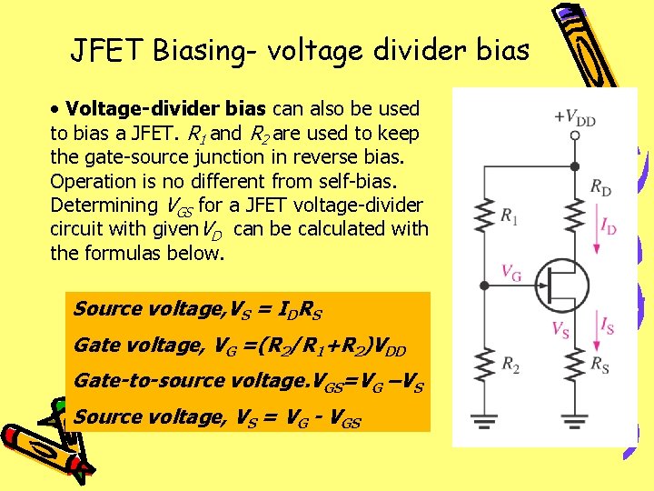
JFET Biasing- voltage divider bias • Voltage-divider bias can also be used to bias a JFET. R 1 and R 2 are used to keep the gate-source junction in reverse bias. Operation is no different from self-bias. Determining VGS for a JFET voltage-divider circuit with given. VD can be calculated with the formulas below. Source voltage, VS = IDRS Gate voltage, VG =(R 2/R 1+R 2)VDD Gate-to-source voltage. VGS=VG –VS Source voltage, VS = VG - VGS

JFET Biasing- voltage-divider bias • VS must be more +ve than VG in order to keep VGS reverse-biased (-ve value). Drain current, ID = (VDD – VD)/RD or Since ID=IS, then ID=VS/RS

MOSFET The metal oxide semiconductor field effect transistor (MOSFET) is the second category of FETs. The difference is that there no pn junction structure instead gate of MOSFET is insulated from the channel by silicon dioxide layer. MOSFETs are static sensitive devices and must be handled by appropriate means. There are depletion MOSFETs (D-MOSFET) and enhancement MOSFETs (E -MOSFET). Note the difference in construction. The E-MOSFET has no structural channel.

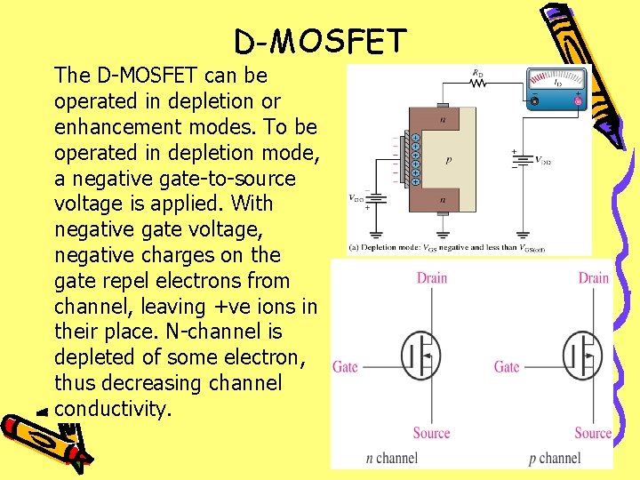
D-MOSFET The D-MOSFET can be operated in depletion or enhancement modes. To be operated in depletion mode, a negative gate-to-source voltage is applied. With negative gate voltage, negative charges on the gate repel electrons from channel, leaving +ve ions in their place. N-channel is depleted of some electron, thus decreasing channel conductivity.

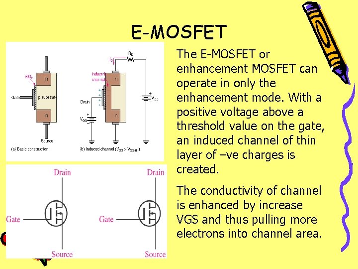
E-MOSFET The E-MOSFET or enhancement MOSFET can operate in only the enhancement mode. With a positive voltage above a threshold value on the gate, an induced channel of thin layer of –ve charges is created. The conductivity of channel is enhanced by increase VGS and thus pulling more electrons into channel area.

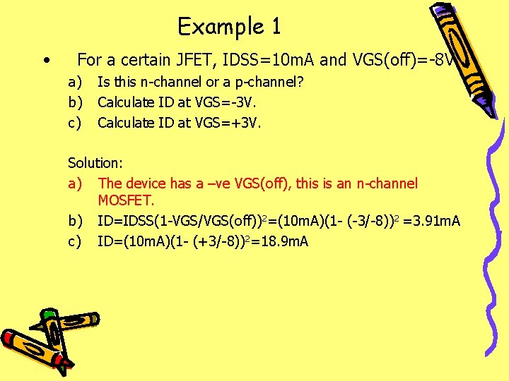
Example 1 • For a certain JFET, IDSS=10 m. A and VGS(off)=-8 V. a) b) c) Is this n-channel or a p-channel? Calculate ID at VGS=-3 V. Calculate ID at VGS=+3 V. Solution: a) The device has a –ve VGS(off), this is an n-channel MOSFET. b) ID=IDSS(1 -VGS/VGS(off))2=(10 m. A)(1 - (-3/-8))2 =3. 91 m. A c) ID=(10 m. A)(1 - (+3/-8))2=18. 9 m. A

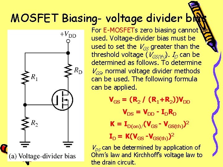
MOSFET Biasing- voltage divider bias For E-MOSFETs zero biasing cannot be used. Voltage-divider bias must be used to set the VGS greater than the threshold voltage (VGS(th)). ID can be determined as follows. To determine VGS, normal voltage divider methods can be used. The following formula can be applied. VGS = (R 2 / (R 1+R 2))VDD VDS = VDD - IDRD K = ID(on)/(VGS - VGS(th))2 ID = K(VGS -VGS(th))2 VDS can be determined by application of Ohm’s law and Kirchhoff’s voltage law to the drain circuit.

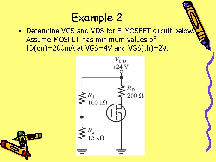
Example 2 • Determine VGS and VDS for E-MOSFET circuit below. Assume MOSFET has minimum values of ID(on)=200 m. A at VGS=4 V and VGS(th)=2 V.

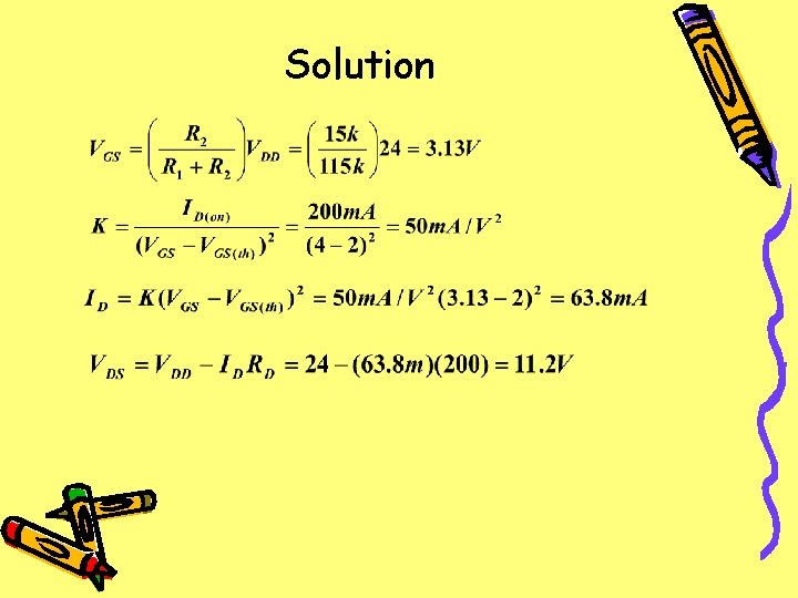
Solution

Troubleshooting As always, having a thorough knowledge of the devices makes for easier troubleshooting circuits utilizing them. We will discuss some the common faults associated with FET circuits. Experience in troubleshooting is the best teacher having basic theoretical knowledge is extremely helpful.

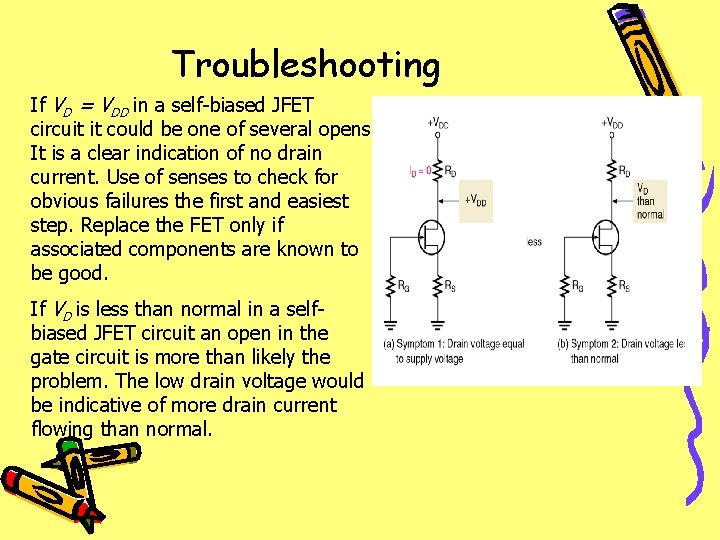
Troubleshooting If VD = VDD in a self-biased JFET circuit it could be one of several opens. It is a clear indication of no drain current. Use of senses to check for obvious failures the first and easiest step. Replace the FET only if associated components are known to be good. If VD is less than normal in a selfbiased JFET circuit an open in the gate circuit is more than likely the problem. The low drain voltage would be indicative of more drain current flowing than normal.

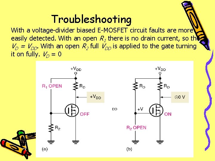
Troubleshooting With a voltage-divider biased E-MOSFET circuit faults are more easily detected. With an open R 1 there is no drain current, so the VD = VDD. With an open R 2 full VDD is applied to the gate turning it on fully. VD = 0

Summary Ø JFETs are unipolar devices. Ø JFETs have three terminals: Source, Gate, and Drain. Ø JFETs have a high input resistance since the gatesource junction is reverse biased. Ø Unwanted capacitance associated with FETs can be dealt with by using dual gate type FETs. Ø IDSS for all FETs is the maximum amount of current flow in the drain circuit when VGS is 0 V.

Summary Ø D-MOSFETs can operate in both depletion and enhancement modes. E-MOSFETs can only operate in the enhancement mode. Ø E-MOSFETs have no physical channel. A channel is induced with VGS greater than VGS(th). Ø E-MOSFETs have no IDSS parameter. Ø There are special MOSFET designs for high power applications.