Chapter 6 Designing Combinational Logic Circuits V 1
Chapter 6 Designing Combinational Logic Circuits V 1. 0 4/25/2003 1 EE 141 Combinational Circu
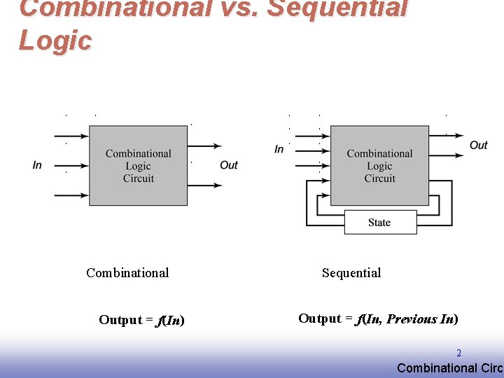
Combinational vs. Sequential Logic Combinational Output = f(In) Sequential Output = f(In, Previous In) 2 EE 141 Combinational Circu
Static CMOS Circuit At every point in time (except during the switching transients) each gate output is connected to either VDD or Vss via a low-resistive path. The outputs of the gates assume at all times the value of the Boolean function, implemented by the circuit (ignoring, once again, the transient effects during switching periods). This is in contrast to the dynamic circuit class, which relies on temporary storage of signal values on the capacitance of high impedance circuit nodes. 3 EE 141 Combinational Circu
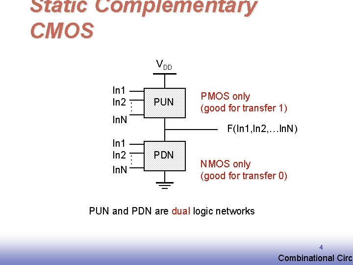
Static Complementary CMOS VDD … In 1 In 2 PUN In. N F(In 1, In 2, …In. N) … In 1 In 2 In. N PMOS only (good for transfer 1) PDN NMOS only (good for transfer 0) PUN and PDN are dual logic networks 4 EE 141 Combinational Circu
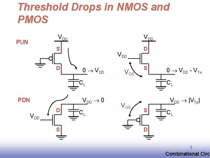
Threshold Drops in NMOS and PMOS VDD PUN VDD S D VDD 0 VDD VGS D S CL VDD 0 PDN VDD D S CL 0 VDD - VTn CL VGS VDD |VTp| S CL D 5 EE 141 Combinational Circu
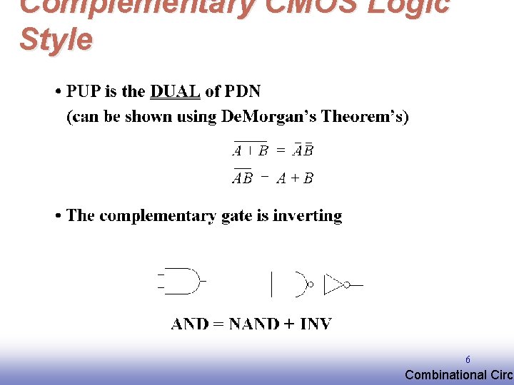
Complementary CMOS Logic Style 6 EE 141 Combinational Circu
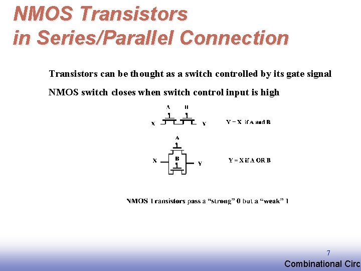
NMOS Transistors in Series/Parallel Connection Transistors can be thought as a switch controlled by its gate signal NMOS switch closes when switch control input is high 7 EE 141 Combinational Circu
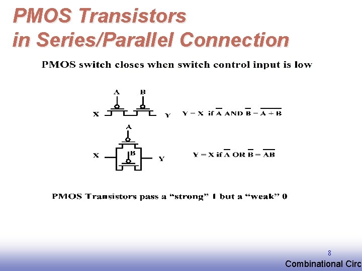
PMOS Transistors in Series/Parallel Connection 8 EE 141 Combinational Circu
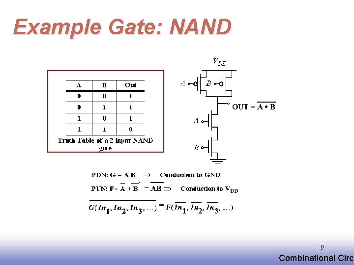
Example Gate: NAND 9 EE 141 Combinational Circu
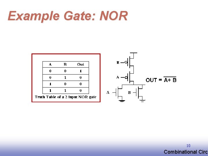
Example Gate: NOR 10 EE 141 Combinational Circu
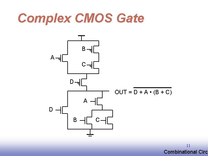
Complex CMOS Gate B A C D OUT = D + A • (B + C) A D B C 11 EE 141 Combinational Circu
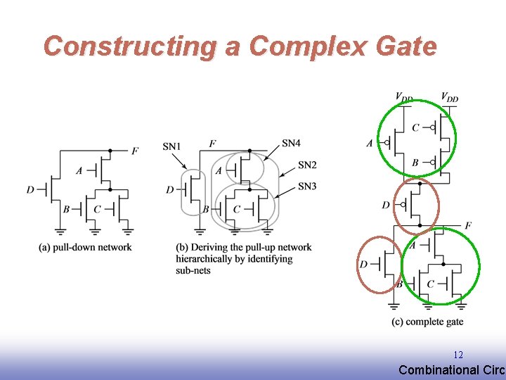
Constructing a Complex Gate 12 EE 141 Combinational Circu
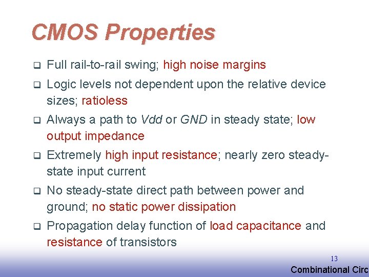
CMOS Properties q Full rail-to-rail swing; high noise margins q Logic levels not dependent upon the relative device sizes; ratioless q Always a path to Vdd or GND in steady state; low output impedance q Extremely high input resistance; nearly zero steadystate input current q No steady-state direct path between power and ground; no static power dissipation q Propagation delay function of load capacitance and resistance of transistors 13 EE 141 Combinational Circu
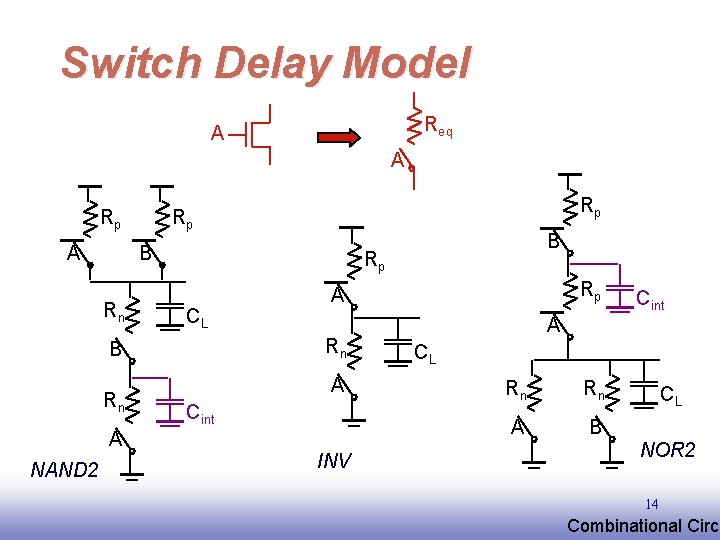
Switch Delay Model Req A A Rp Rp B Rn Rp CL A Cint A NAND 2 Rp A Rn B INV Cint A CL Rn Rn A B CL NOR 2 14 EE 141 Combinational Circu
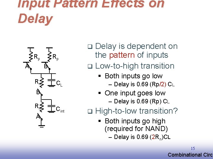
Input Pattern Effects on Delay is dependent on the pattern of inputs q Low-to-high transition q Rp A Rp B Rn § Both inputs go low CL – Delay is 0. 69 (Rp/2) CL § One input goes low B Rn A – Delay is 0. 69 (Rp) CL Cint q High-to-low transition? § Both inputs go high (required for NAND) – Delay is 0. 69 (2 Rn)CL 15 EE 141 Combinational Circu
![Delay Dependence on Input Patterns A=B=1 0 Voltage [V] A=1 0, B=1 A=1, B=1 Delay Dependence on Input Patterns A=B=1 0 Voltage [V] A=1 0, B=1 A=1, B=1](http://slidetodoc.com/presentation_image_h2/17029e17bf61bc7dff555fed1d55b7f0/image-16.jpg)
Delay Dependence on Input Patterns A=B=1 0 Voltage [V] A=1 0, B=1 A=1, B=1 0 time [ps] A=1, B=1 0 (for both Cint and CL) EE 141 Input Data Pattern Delay (psec) A=B=0 1 69 A=1, B=0 1 62 A= 0 1, B=1 50 A=B=1 0 35 A=1, B=1 0 76 A= 1 0, B=1 57 NMOS = 0. 5 m/0. 25 m PMOS = 0. 75 m/0. 25 m CL = 100 f. F 16 Combinational Circu
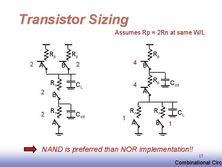
Transistor Sizing Assumes Rp = 2 Rn at same W/L Rp 2 A Rp B Rn 2 B 2 Rn A Rp 4 B 2 CL Cint 4 1 Rp Cint A Rn Rn A B CL 1 NAND is preferred than NOR implementation!! 17 EE 141 Combinational Circu
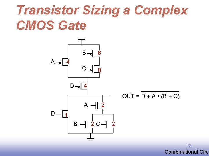
Transistor Sizing a Complex CMOS Gate A B 8 C 8 4 D 4 OUT = D + A • (B + C) A D 2 1 B 2 C 2 18 EE 141 Combinational Circu
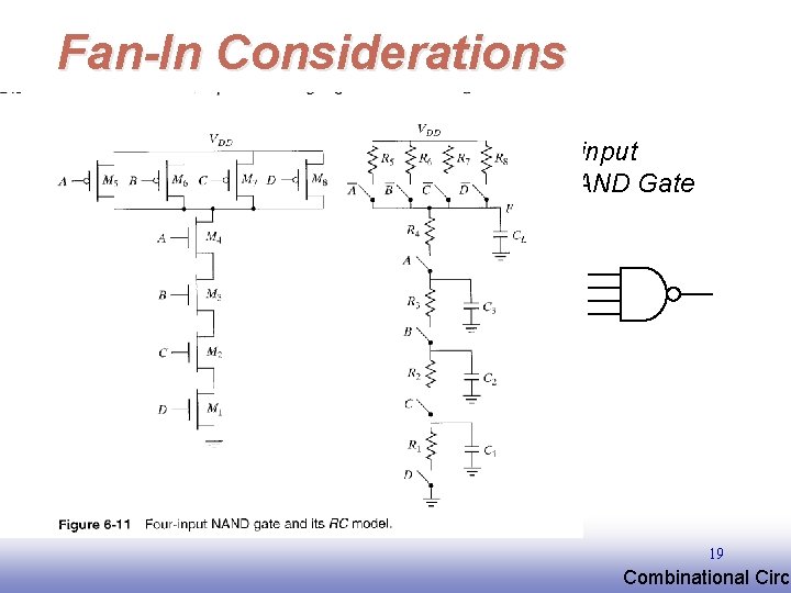
Fan-In Considerations 4 -input NAND Gate 19 EE 141 Combinational Circu
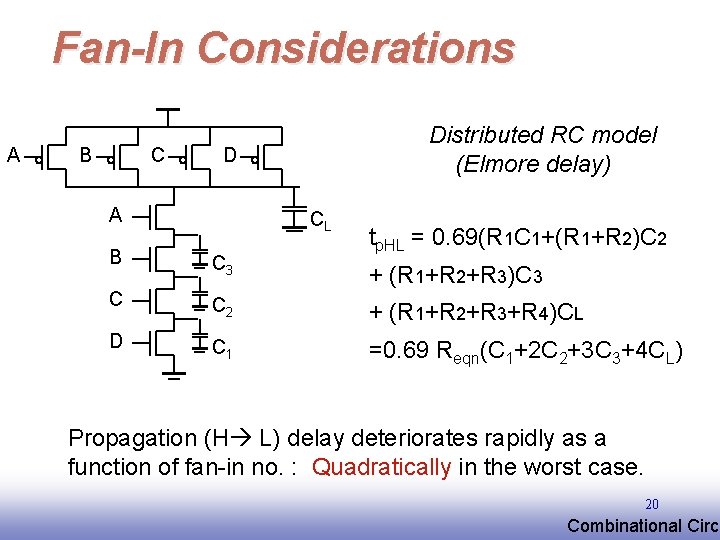
Fan-In Considerations A B C Distributed RC model (Elmore delay) D A CL tp. HL = 0. 69(R 1 C 1+(R 1+R 2)C 2 B C 3 C C 2 + (R 1+R 2+R 3+R 4)CL D C 1 =0. 69 Reqn(C 1+2 C 2+3 C 3+4 CL) + (R 1+R 2+R 3)C 3 Propagation (H L) delay deteriorates rapidly as a function of fan-in no. : Quadratically in the worst case. 20 EE 141 Combinational Circu
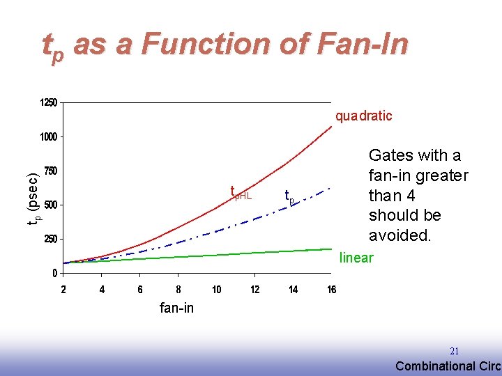
tp as a Function of Fan-In tp (psec) quadratic tp. HL tp tp. LH Gates with a fan-in greater than 4 should be avoided. linear fan-in 21 EE 141 Combinational Circu
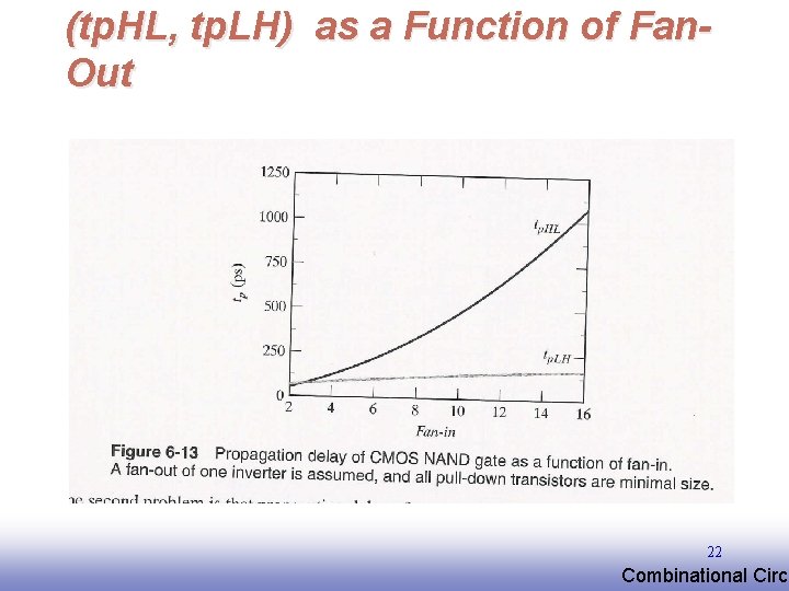
(tp. HL, tp. LH) as a Function of Fan. Out 22 EE 141 Combinational Circu
tp as a Function of Fan-In and Fan-Out q Fan-in: quadratic due to increasing resistance and capacitance q Fan-out: each additional fan-out gate adds two gate capacitances to CL 23 EE 141 Combinational Circu
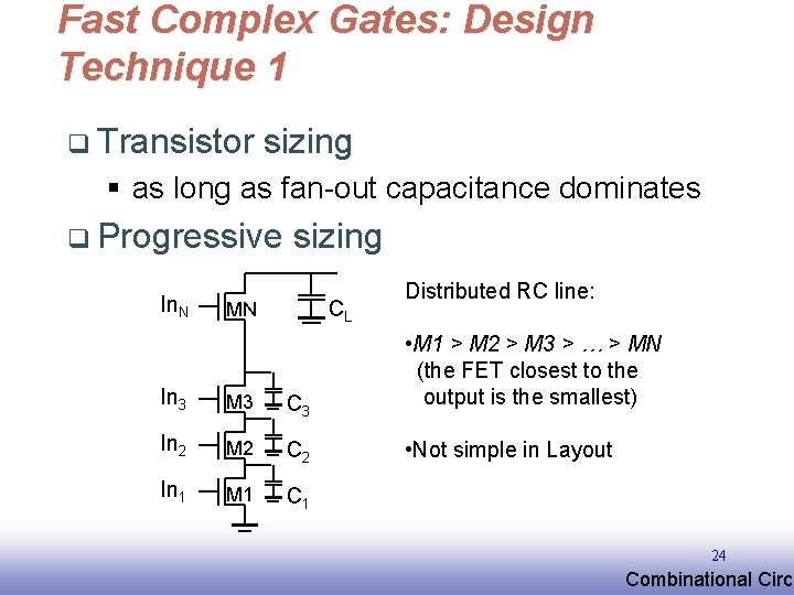
Fast Complex Gates: Design Technique 1 q Transistor sizing § as long as fan-out capacitance dominates q Progressive In. N sizing CL MN Distributed RC line: In 3 M 3 C 3 • M 1 > M 2 > M 3 > … > MN (the FET closest to the output is the smallest) In 2 M 2 C 2 • Not simple in Layout In 1 M 1 C 1 24 EE 141 Combinational Circu
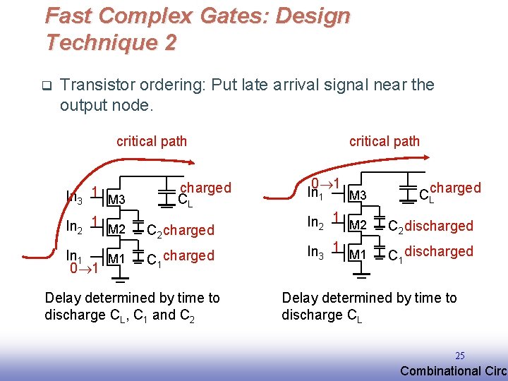
Fast Complex Gates: Design Technique 2 q Transistor ordering: Put late arrival signal near the output node. critical path In 3 1 M 3 charged CL In 2 1 M 2 C 2 charged In 1 M 1 0 1 C 1 charged Delay determined by time to discharge CL, C 1 and C 2 critical path 0 1 In 1 M 3 CLcharged In 2 1 M 2 C 2 discharged In 3 1 M 1 C 1 discharged Delay determined by time to discharge CL 25 EE 141 Combinational Circu
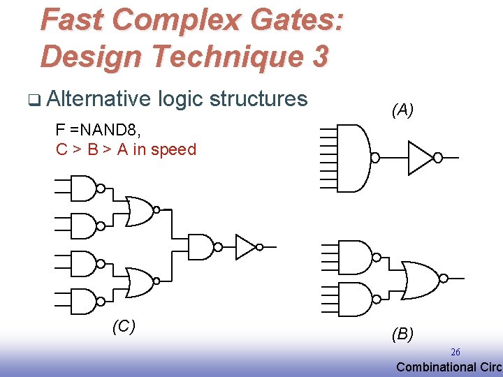
Fast Complex Gates: Design Technique 3 q Alternative logic structures (A) F =NAND 8, C > B > A in speed (C) (B) 26 EE 141 Combinational Circu
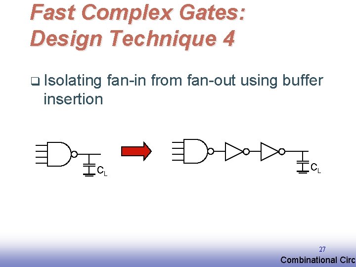
Fast Complex Gates: Design Technique 4 q Isolating fan-in from fan-out using buffer insertion CL CL 27 EE 141 Combinational Circu
Sizing Logic Paths for Speed Frequently, input capacitance of a logic path is constrained q Logic also has to drive some capacitance q Example: ALU load in an Intel’s microprocessor is 0. 5 p. F q How do we size the ALU datapath to achieve maximum speed? q We have already solved this for the inverter chain – can we generalize it for any type of logic? q 28 EE 141 Combinational Circu
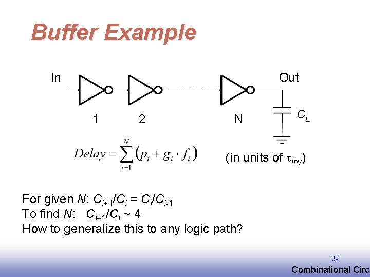
Buffer Example In Out 1 2 N CL (in units of tinv) For given N: Ci+1/Ci = Ci/Ci-1 To find N: Ci+1/Ci ~ 4 How to generalize this to any logic path? 29 EE 141 Combinational Circu
Logical Effort Inverter has the smallest logical effort and intrinsic delay of all static CMOS gates q Logical effort of a gate presents the ratio of its input capacitance to the inverter capacitance when sized to deliver the same current q Logical effort increases with the gate complexity q 30 EE 141 Combinational Circu
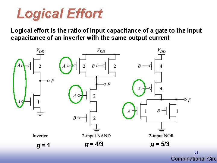
Logical Effort Logical effort is the ratio of input capacitance of a gate to the input capacitance of an inverter with the same output current g=1 g = 4/3 g = 5/3 31 EE 141 Combinational Circu
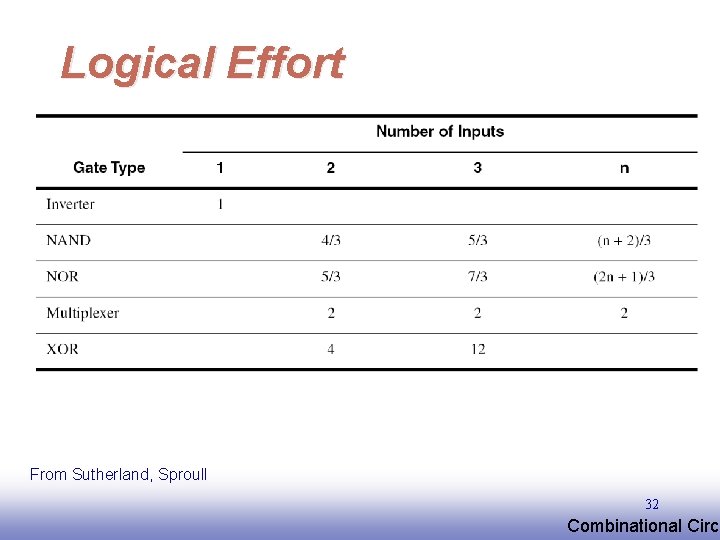
Logical Effort From Sutherland, Sproull 32 EE 141 Combinational Circu
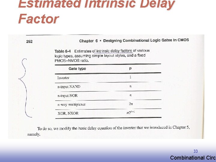
Estimated Intrinsic Delay Factor 33 EE 141 Combinational Circu
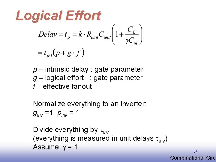
Logical Effort p – intrinsic delay : gate parameter g – logical effort : gate parameter f – effective fanout Normalize everything to an inverter: ginv =1, pinv = 1 Divide everything by tinv (everything is measured in unit delays tinv) Assume g = 1. EE 141 34 Combinational Circu
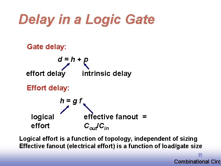
Delay in a Logic Gate delay: d=h+p effort delay intrinsic delay Effort delay: h=gf logical effort effective fanout = Cout/Cin Logical effort is a function of topology, independent of sizing Effective fanout (electrical effort) is a function of load/gate size 35 EE 141 Combinational Circu
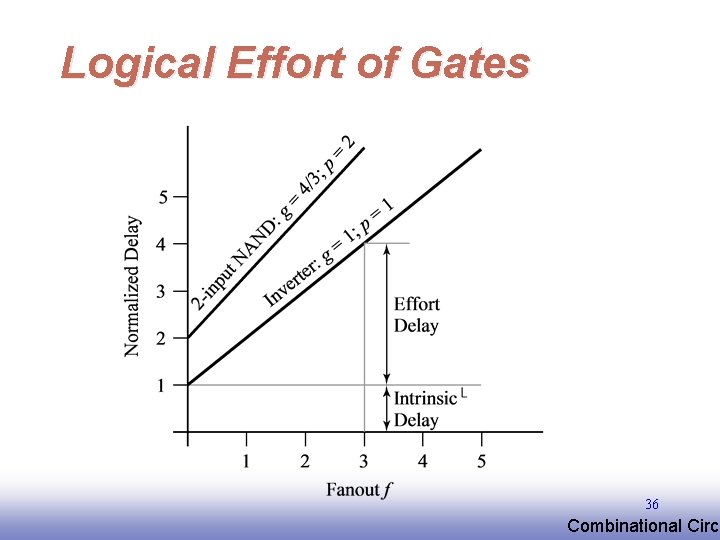
Logical Effort of Gates 36 EE 141 Combinational Circu
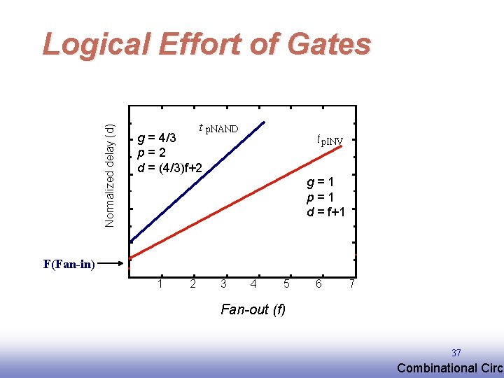
Normalized delay (d) Logical Effort of Gates t p. NAND g = 4/3 p=2 d = (4/3)f+2 t p. INV g=1 p=1 d = f+1 F(Fan-in) 1 2 3 4 5 6 7 Fan-out (f) 37 EE 141 Combinational Circu
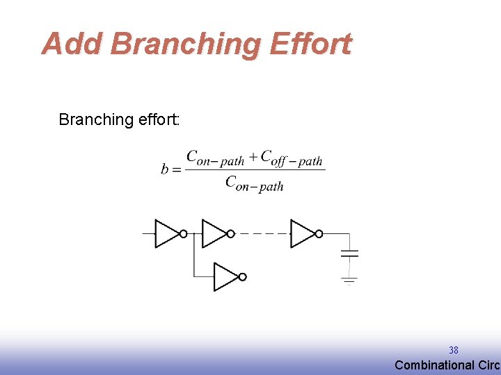
Add Branching Effort Branching effort: 38 EE 141 Combinational Circu
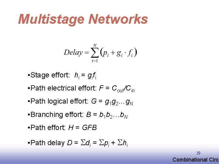
Multistage Networks • Stage effort: hi = gifi • Path electrical effort: F = Cout/Cin • Path logical effort: G = g 1 g 2…g. N • Branching effort: B = b 1 b 2…b. N • Path effort: H = GFB • Path delay D = Sdi = Spi + Shi 39 EE 141 Combinational Circu
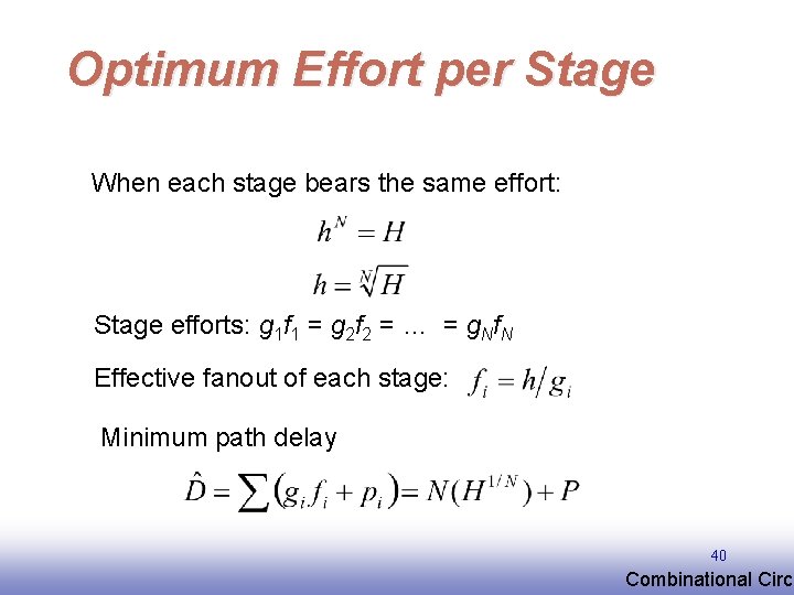
Optimum Effort per Stage When each stage bears the same effort: Stage efforts: g 1 f 1 = g 2 f 2 = … = g. Nf. N Effective fanout of each stage: Minimum path delay 40 EE 141 Combinational Circu
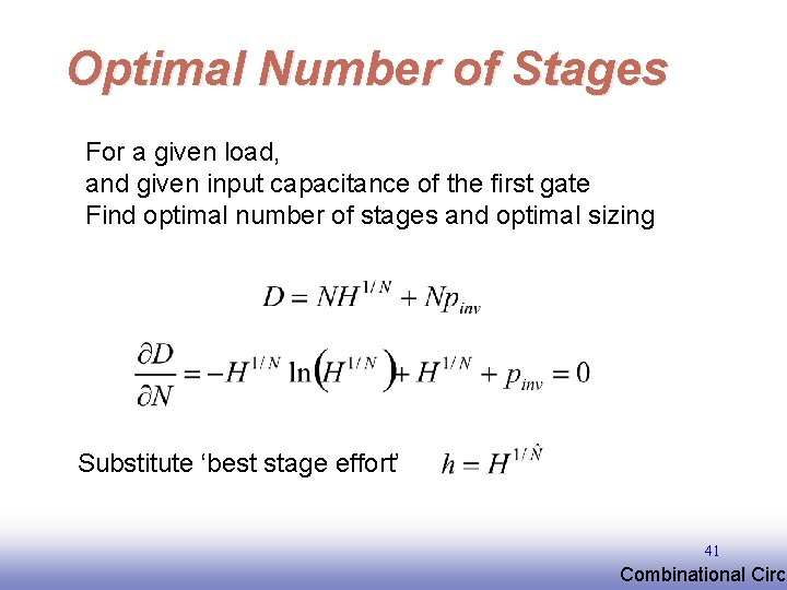
Optimal Number of Stages For a given load, and given input capacitance of the first gate Find optimal number of stages and optimal sizing Substitute ‘best stage effort’ 41 EE 141 Combinational Circu
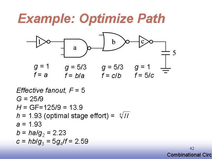
Example: Optimize Path g=1 f=a g = 5/3 f = b/a g = 5/3 f = c/b Effective fanout, F = 5 G = 25/9 H = GF=125/9 = 13. 9 h = 1. 93 (optimal stage effort) = a = 1. 93 b = ha/g 2 = 2. 23 c = hb/g 3 = 5 g 4/f = 2. 59 EE 141 g=1 f = 5/c 42 Combinational Circu
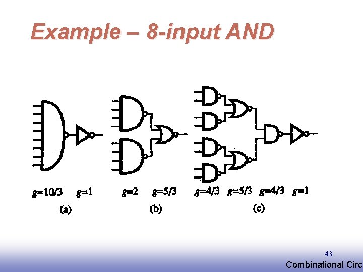
Example – 8 -input AND 43 EE 141 Combinational Circu
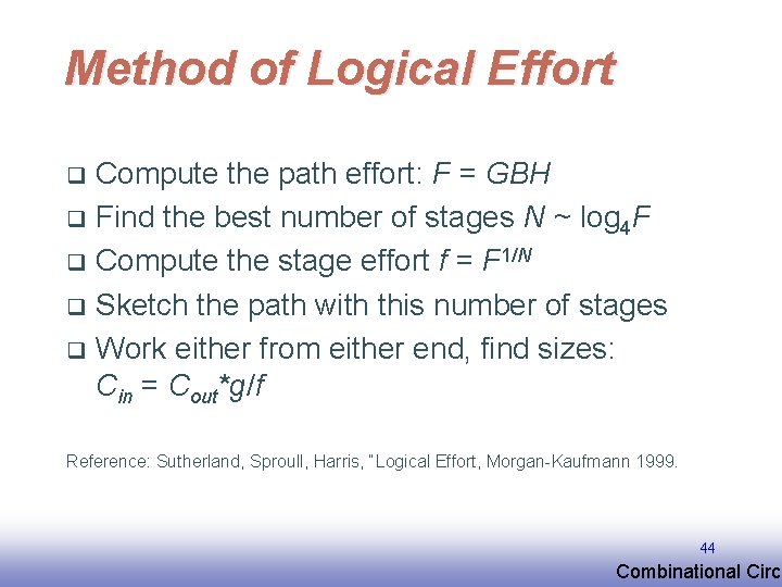
Method of Logical Effort Compute the path effort: F = GBH q Find the best number of stages N ~ log 4 F q Compute the stage effort f = F 1/N q Sketch the path with this number of stages q Work either from either end, find sizes: Cin = Cout*g/f q Reference: Sutherland, Sproull, Harris, “Logical Effort, Morgan-Kaufmann 1999. 44 EE 141 Combinational Circu
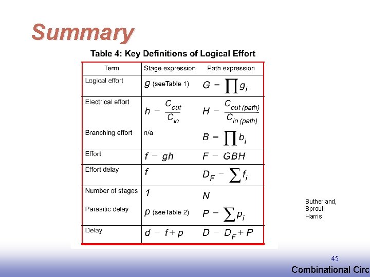
Summary Sutherland, Sproull Harris 45 EE 141 Combinational Circu
Pass. Transistor Logic 46 EE 141 Combinational Circu
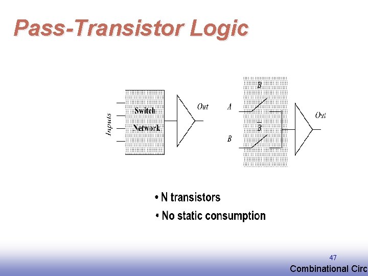
Pass-Transistor Logic 47 EE 141 Combinational Circu
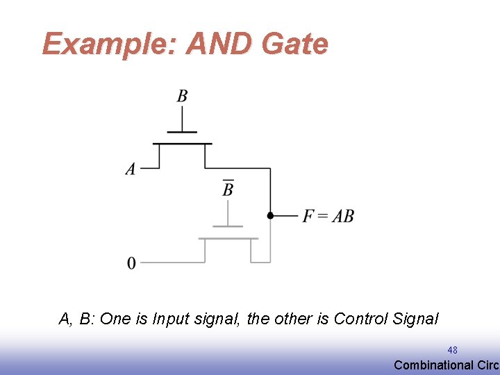
Example: AND Gate A, B: One is Input signal, the other is Control Signal 48 EE 141 Combinational Circu
![NMOS-Only Logic 3. 0 Voltage [V] In Out 2. 0 x 1. 0 0 NMOS-Only Logic 3. 0 Voltage [V] In Out 2. 0 x 1. 0 0](http://slidetodoc.com/presentation_image_h2/17029e17bf61bc7dff555fed1d55b7f0/image-49.jpg)
NMOS-Only Logic 3. 0 Voltage [V] In Out 2. 0 x 1. 0 0 0. 5 1 1. 5 2 Time [ns] 49 EE 141 Combinational Circu
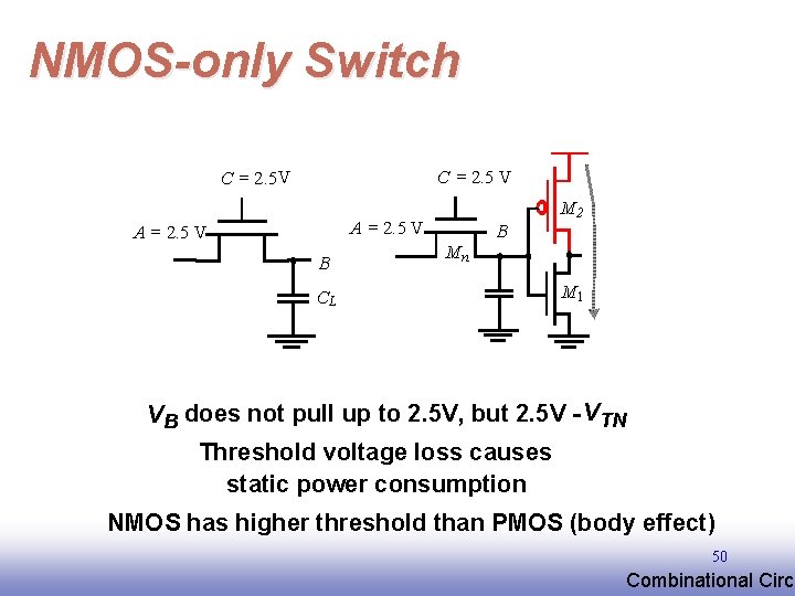
NMOS-only Switch C = 2. 5 V C = 2. 5 V A = 2. 5 V B B M 2 Mn CL M 1 VB does not pull up to 2. 5 V, but 2. 5 V - VTN Threshold voltage loss causes static power consumption NMOS has higher threshold than PMOS (body effect) 50 EE 141 Combinational Circu
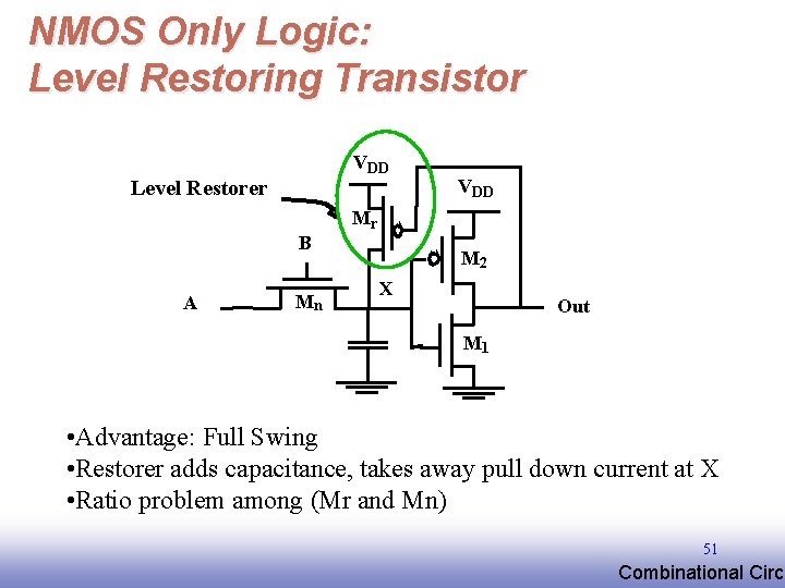
NMOS Only Logic: Level Restoring Transistor VDD Level Restorer VDD Mr B A Mn M 2 X Out M 1 • Advantage: Full Swing • Restorer adds capacitance, takes away pull down current at X • Ratio problem among (Mr and Mn) 51 EE 141 Combinational Circu
![Restorer Sizing Voltage [V] 3. 0 2. 0 W/Lr =1. 75/0. 25 W/L r Restorer Sizing Voltage [V] 3. 0 2. 0 W/Lr =1. 75/0. 25 W/L r](http://slidetodoc.com/presentation_image_h2/17029e17bf61bc7dff555fed1d55b7f0/image-52.jpg)
Restorer Sizing Voltage [V] 3. 0 2. 0 W/Lr =1. 75/0. 25 W/L r =1. 50/0. 25 • Upper limit on restorer size • Pass-transistor pull-down can have several transistors in stack 1. 0 W/Lr =1. 0/0. 25 0. 0 0 100 200 W/L r =1. 25/0. 25 300 Time [ps] 400 52 EE 141 Combinational Circu
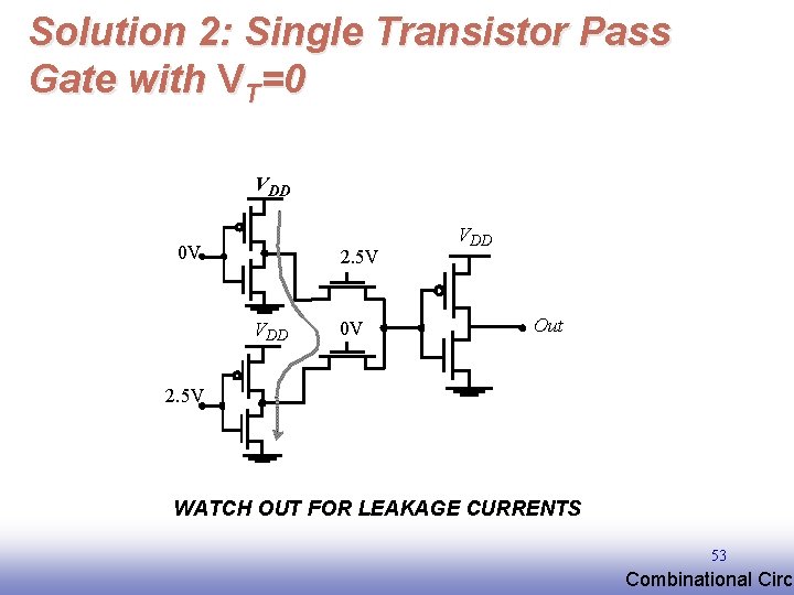
Solution 2: Single Transistor Pass Gate with VT=0 VDD 0 V 2. 5 V VDD 0 V VDD Out 2. 5 V WATCH OUT FOR LEAKAGE CURRENTS 53 EE 141 Combinational Circu
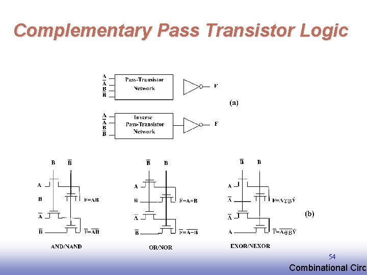
Complementary Pass Transistor Logic 54 EE 141 Combinational Circu
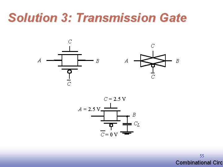
Solution 3: Transmission Gate C A B B C C C = 2. 5 V A = 2. 5 V B CL C=0 V 55 EE 141 Combinational Circu
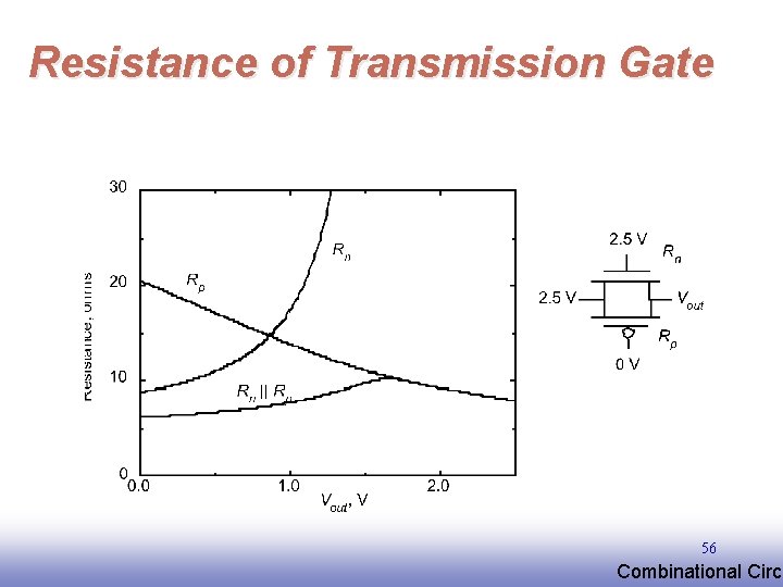
Resistance of Transmission Gate 56 EE 141 Combinational Circu
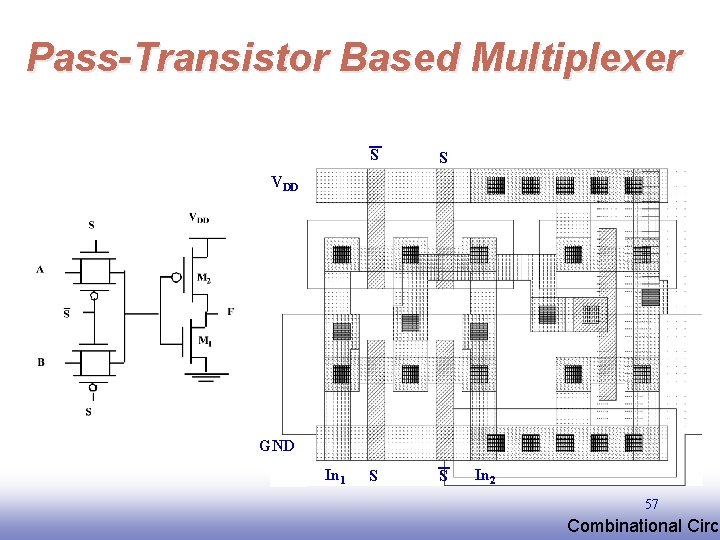
Pass-Transistor Based Multiplexer S S VDD GND In 1 In 2 57 EE 141 Combinational Circu
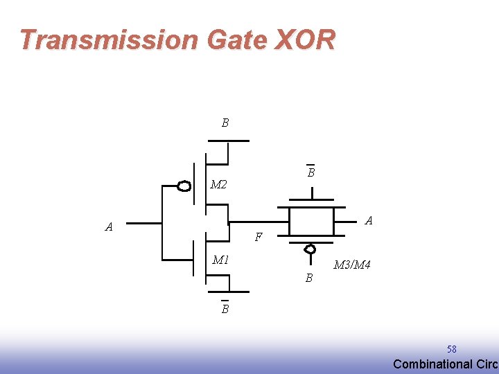
Transmission Gate XOR B B M 2 A A F M 1 B M 3/M 4 B 58 EE 141 Combinational Circu
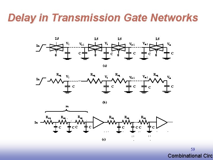
Delay in Transmission Gate Networks 2. 5 V 1 In 2. 5 Vi Vi-1 C 0 2. 5 C 0 Vn-1 Vi+1 C 0 Vn C C 0 (a) Req In Req V 1 Req Vi C Vn-1 Vi+1 C C Req Vn C C (b) m Req Req Req In C CC C (c) 59 EE 141 Combinational Circu
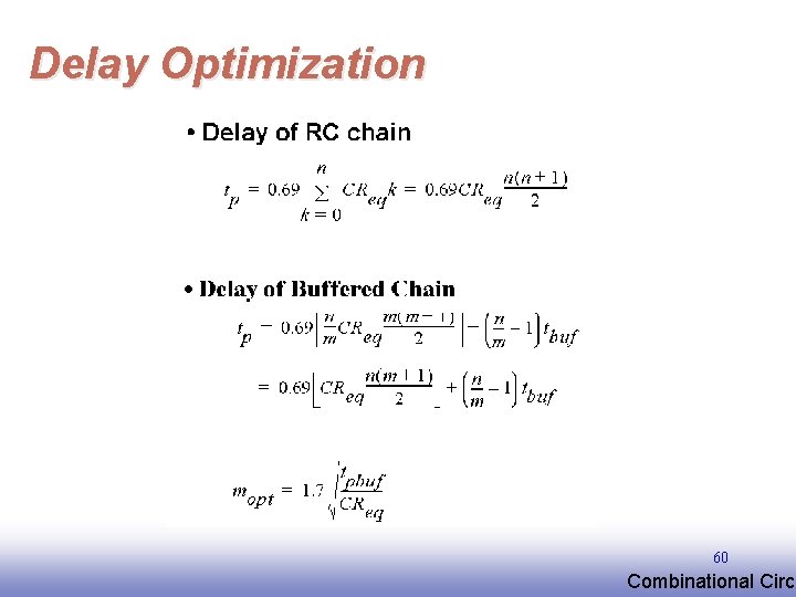
Delay Optimization 60 EE 141 Combinational Circu
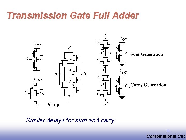
Transmission Gate Full Adder Similar delays for sum and carry 61 EE 141 Combinational Circu
Dynamic Logic 62 EE 141 Combinational Circu
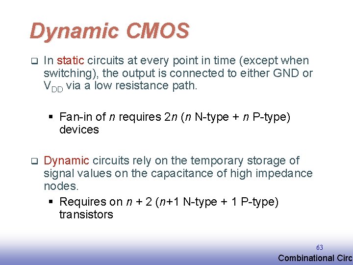
Dynamic CMOS q In static circuits at every point in time (except when switching), the output is connected to either GND or VDD via a low resistance path. § Fan-in of n requires 2 n (n N-type + n P-type) devices q Dynamic circuits rely on the temporary storage of signal values on the capacitance of high impedance nodes. § Requires on n + 2 (n+1 N-type + 1 P-type) transistors 63 EE 141 Combinational Circu
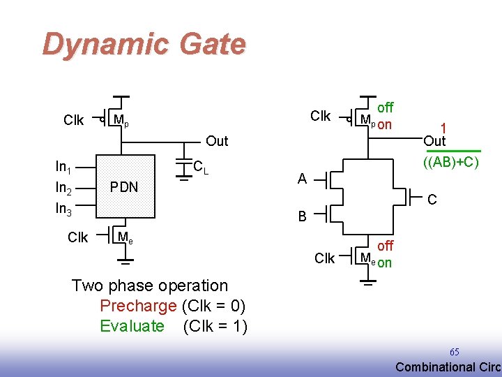
Dynamic Gate Clk Mp off Mp on Out In 1 In 2 In 3 Clk CL PDN 1 Out ((AB)+C) A C B Me Clk off Me on Two phase operation Precharge (Clk = 0) Evaluate (Clk = 1) 65 EE 141 Combinational Circu
Conditions on Output Once the output of a dynamic gate is discharged, it cannot be charged again until the next precharge operation. q Inputs to the gate can make at most one transition during evaluation. q q Output can be in the high impedance state during and after evaluation (PDN off), state is stored on CL 66 EE 141 Combinational Circu
Properties of Dynamic Gates q Logic function is implemented by the PDN only § number of transistors is N + 2 (versus 2 N for static complementary CMOS) Full swing outputs (VOL = GND and VOH = VDD) q Non-ratioed - sizing of the devices does not affect the logic levels q Faster switching speeds q § reduced load capacitance due to lower input capacitance (Cin) § reduced load capacitance due to smaller output loading (Cout) § no Isc, so all the current provided by PDN goes into discharging CL 67 EE 141 Combinational Circu
Properties of Dynamic Gates q Overall power dissipation usually higher than static CMOS § no static current path ever exists between VDD and GND (including Psc) § no glitching § Higher transition probabilities § Extra load on Clk q PDN starts to work as soon as the input signals exceed VTn, so VM, VIH and VIL equal to VTn § Low noise margin (NML) q Needs a precharge/evaluate clock 68 EE 141 Combinational Circu
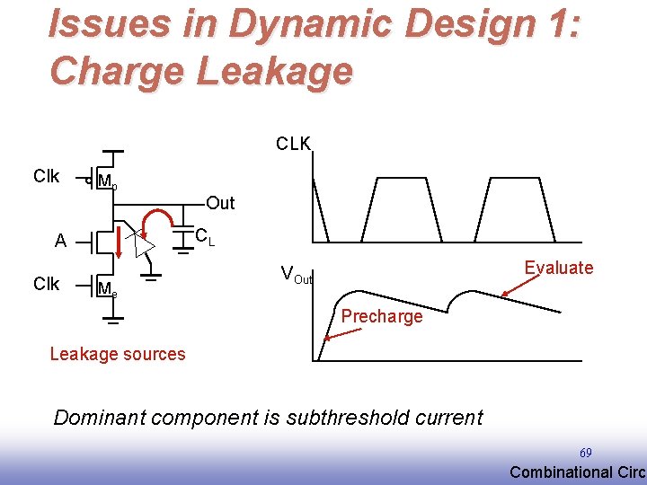
Issues in Dynamic Design 1: Charge Leakage CLK Clk Mp Out CL A Clk Me Evaluate VOut Precharge Leakage sources Dominant component is subthreshold current 69 EE 141 Combinational Circu

Solution to Charge Leakage Keeper Clk Mp A Mkp CL Out B Clk Me Same approach as level restorer for pass-transistor logic 70 EE 141 Combinational Circu
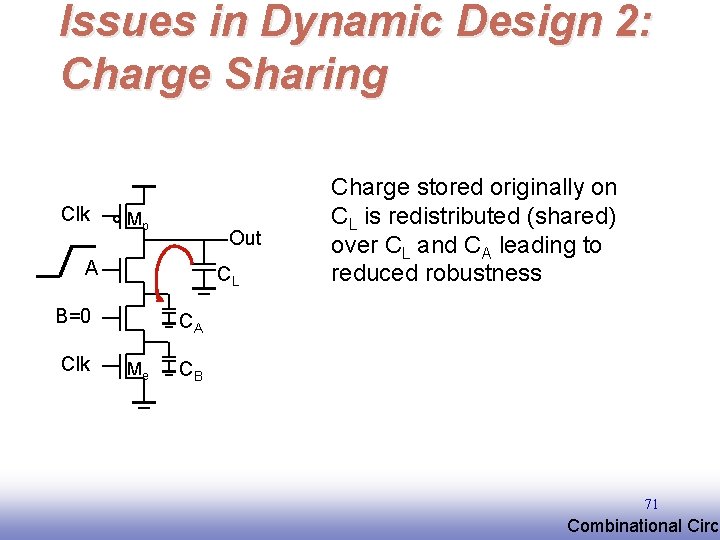
Issues in Dynamic Design 2: Charge Sharing Clk Mp Out A CL B=0 Clk Charge stored originally on CL is redistributed (shared) over CL and CA leading to reduced robustness CA Me CB 71 EE 141 Combinational Circu
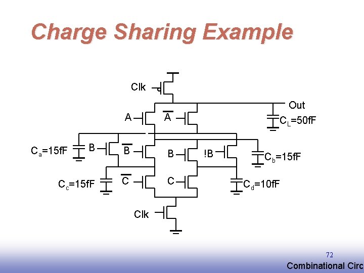
Charge Sharing Example Clk A A B B B Cc=15 f. F C C Ca=15 f. F Out CL=50 f. F !B Cb=15 f. F Cd=10 f. F Clk 72 EE 141 Combinational Circu
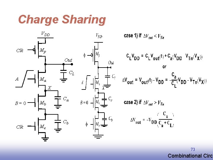
Charge Sharing VDD Clk Mp Out CL A Ma X B=0 Clk Mb Me Ca Cb 73 EE 141 Combinational Circu
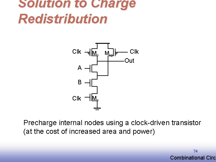
Solution to Charge Redistribution Clk Mp Mkp Clk Out A B Clk Me Precharge internal nodes using a clock-driven transistor (at the cost of increased area and power) 74 EE 141 Combinational Circu
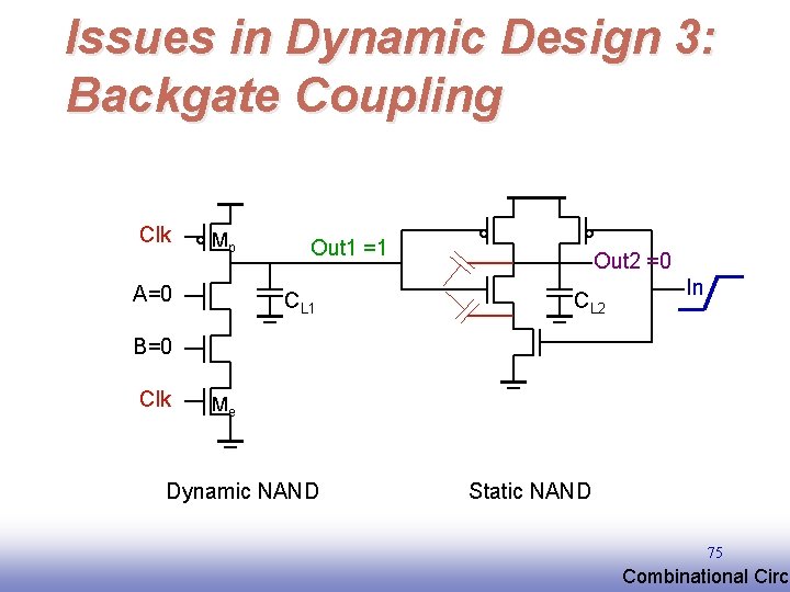
Issues in Dynamic Design 3: Backgate Coupling Clk Mp A=0 Out 1 =1 CL 1 Out 2 =0 CL 2 In B=0 Clk Me Dynamic NAND Static NAND 75 EE 141 Combinational Circu
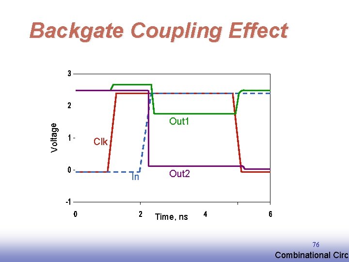
Voltage Backgate Coupling Effect Out 1 Clk In Out 2 Time, ns 76 EE 141 Combinational Circu
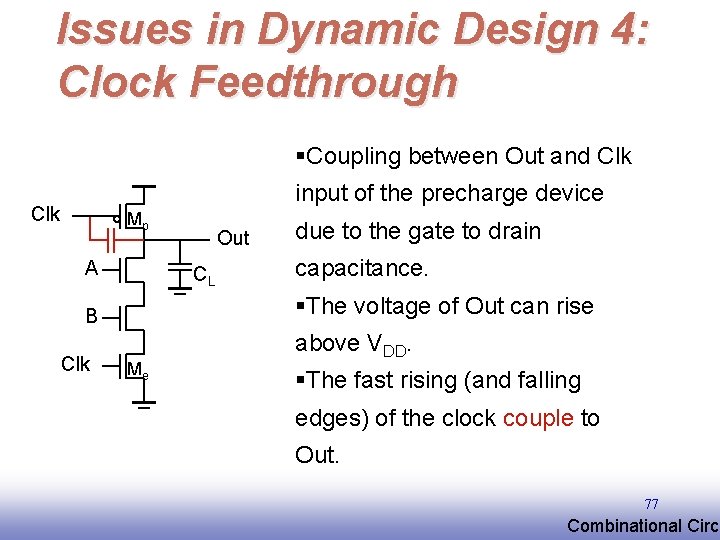
Issues in Dynamic Design 4: Clock Feedthrough §Coupling between Out and Clk input of the precharge device Clk Mp A CL due to the gate to drain capacitance. §The voltage of Out can rise B Clk Out Me above VDD. §The fast rising (and falling edges) of the clock couple to Out. 77 EE 141 Combinational Circu

Clock Feedthrough Clock feedthrough Clk Out In 1 In 3 In 4 Voltage In 2 In & Clk Out Clk Time, ns Clock feedthrough 78 EE 141 Combinational Circu
Other Effects q Capacitive coupling q Substrate coupling q Minority charge injection q Supply noise (ground bounce) 79 EE 141 Combinational Circu
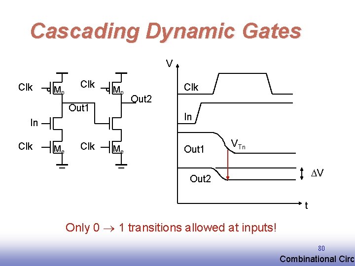
Cascading Dynamic Gates V Clk Mp Out 1 Me Clk Out 2 In In Clk Me Out 1 VTn V Out 2 t Only 0 1 transitions allowed at inputs! 80 EE 141 Combinational Circu
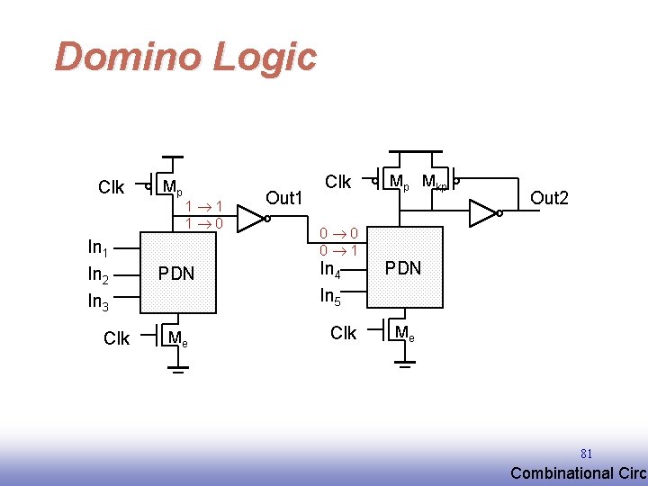
Domino Logic Clk In 1 In 2 In 3 Clk Mp 1 1 1 0 PDN Me Out 1 Clk 0 0 0 1 In 4 In 5 Clk Mp Mkp Out 2 PDN Me 81 EE 141 Combinational Circu
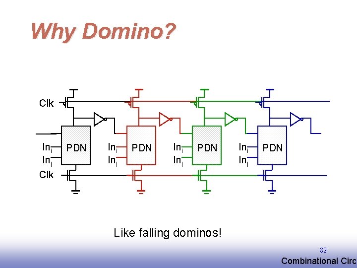
Why Domino? Clk Ini Inj Clk PDN Ini Inj PDN Like falling dominos! 82 EE 141 Combinational Circu
Properties of Domino Logic Only non-inverting logic can be implemented q Very high speed q § static inverter can be skewed, only L-H transition § Input capacitance reduced – smaller logical effort 83 EE 141 Combinational Circu
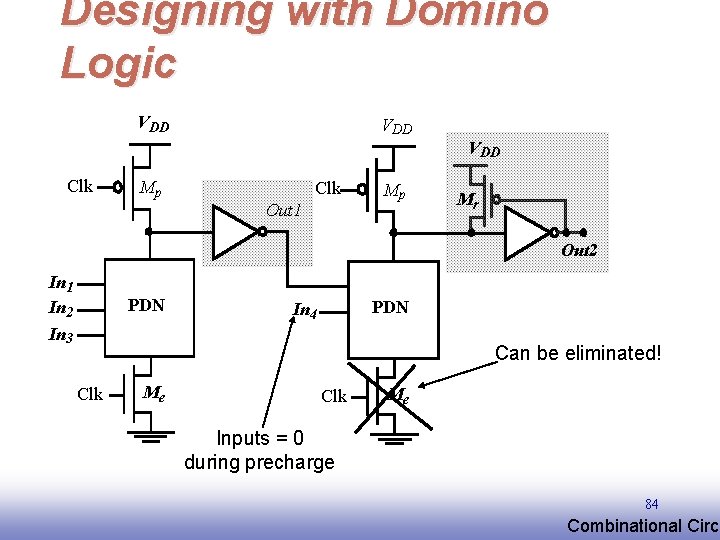
Designing with Domino Logic VDD VDD Clk Mp Clk Out 1 Mp Mr Out 2 In 1 In 2 In 3 PDN In 4 Can be eliminated! Clk Me Inputs = 0 during precharge 84 EE 141 Combinational Circu
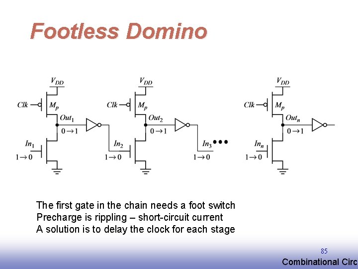
Footless Domino The first gate in the chain needs a foot switch Precharge is rippling – short-circuit current A solution is to delay the clock for each stage 85 EE 141 Combinational Circu
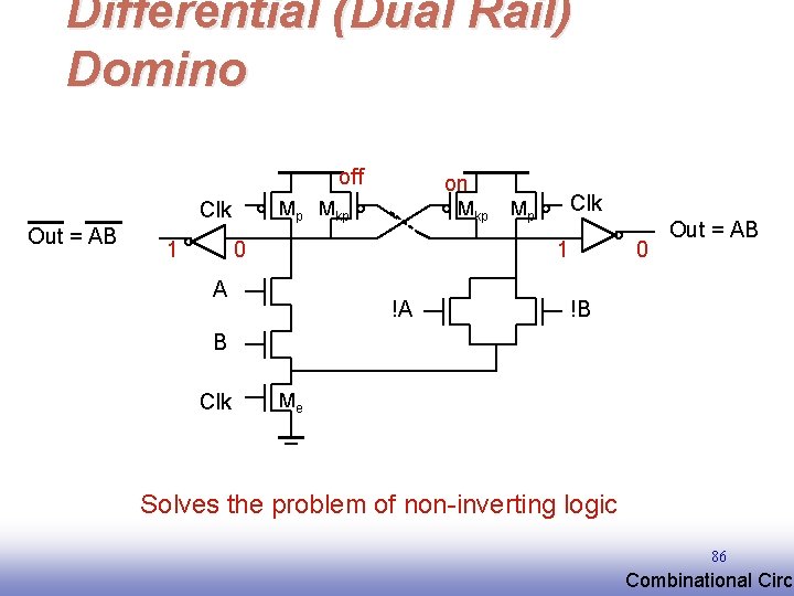
Differential (Dual Rail) Domino off Mp Mkp Clk Out = AB 1 on Mkp 0 Clk Mp 1 A !A 0 Out = AB !B B Clk Me Solves the problem of non-inverting logic 86 EE 141 Combinational Circu
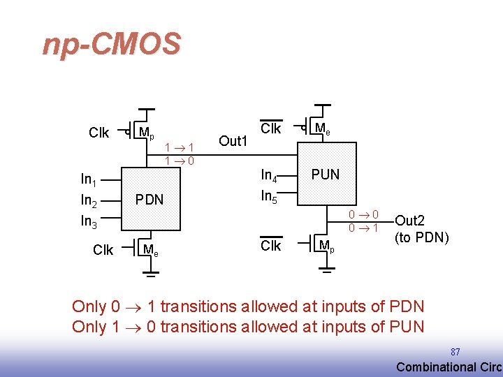
np-CMOS Clk In 1 In 2 In 3 Clk Mp 1 1 1 0 PDN Me Out 1 Clk Me In 4 In 5 PUN 0 0 0 1 Clk Mp Out 2 (to PDN) Only 0 1 transitions allowed at inputs of PDN Only 1 0 transitions allowed at inputs of PUN 87 EE 141 Combinational Circu
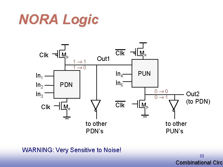
NORA Logic Clk In 1 In 2 In 3 Clk Mp 1 1 1 0 Out 1 PDN Clk Me In 4 In 5 PUN 0 0 0 1 Clk Me to other PDN’s Mp Out 2 (to PDN) to other PUN’s WARNING: Very Sensitive to Noise! 88 EE 141 Combinational Circu
- Slides: 87