Chapter 6 Bipolar Junction Transistors BJTs Bipolar Junction
")
Chapter 6. Bipolar Junction Transistors (BJTs)

Bipolar Junction Transistor • Three terminal device • Voltage between two terminals to control current flow in third terminal • Invented in 1948 at Bell Telephone Laboratories • Dominant until late 1980’s • Reliable under harsh operating conditions – High frequency applications – High speed designs – High power applications
 region, p-type base (B) region, n-type collector (C)")
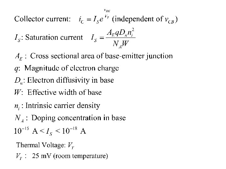
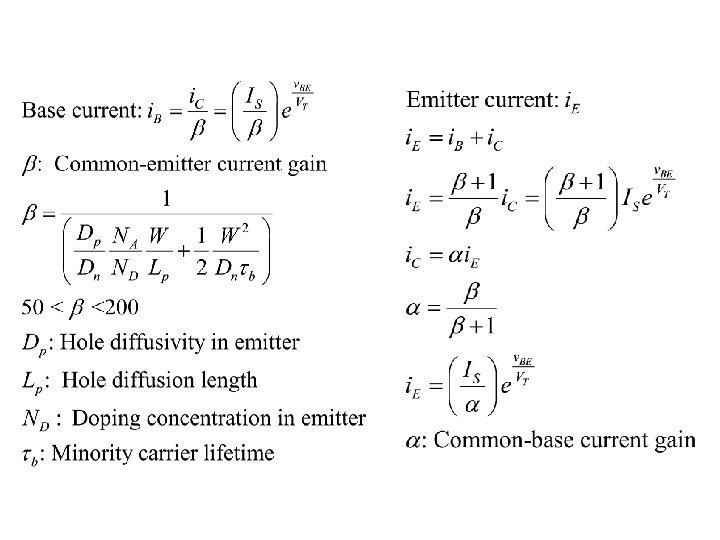
npn transistor • n-type emitter (E) region, p-type base (B) region, n-type collector (C) region • Two pn junctions (naming basis for bipolar junction transistor) • Modes - Active: used for amplifier design - Cutoff - Saturation: used for logic design - Reverse active: limited operation

pnp transistor – dual of npn transistor

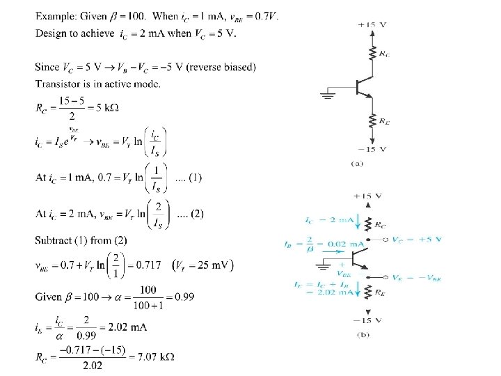
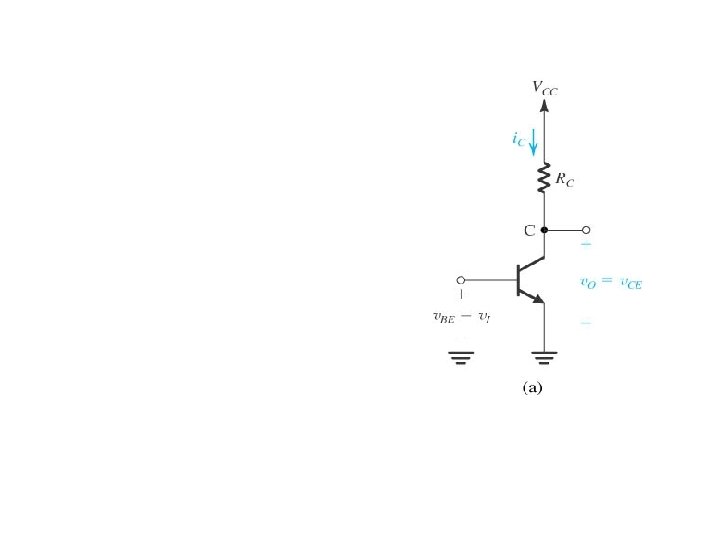
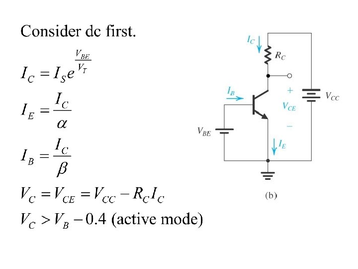
Active Mode of npn Transistor

Circuit Models for Active Mode npn Transistor

Practical Implementation E and C are not symmetrical. pnp transistors works dual to npn transistors much in the same way PMOSFET works dual to NMOSFET. (In this class, we will concentrate on npn transistors. )

Circuit Symbols for npn Transistors Biasing in active mode Directions of current flow

i. C – v. BE Characteristics Temperature Dependence

Common Base Characteristics Base voltage is fixed at zero. In active region, v. CB ≥ - 0. 4 V

Dependence of i. C on Collector Voltage

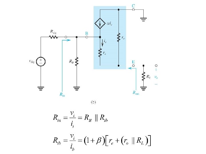
Circuit Models with Output Resistance ro

Common Emitter Configuration
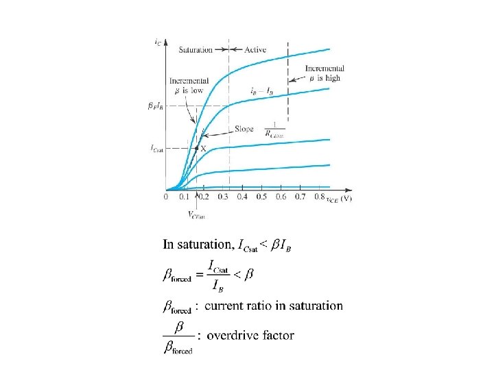

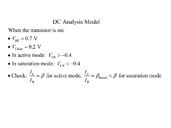
Common Emitter Saturation Model
")
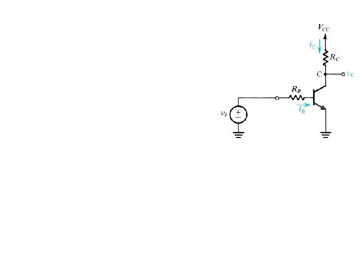
Designing Linear Amplifiers (Active Region)

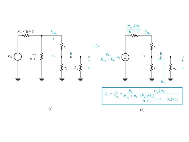
Amplifier Gain

Graphical Analysis
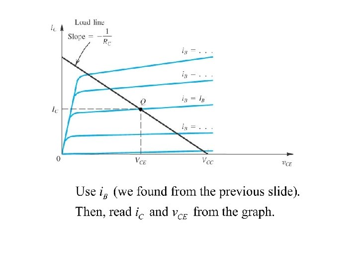

To determine i. B, i. C and v. CE, you need to use both graphs.

Quiescent point must be selected to give a symmetric output swing.


Input part 10 V RB 1 VBB RB 2 10 V +_ RB 2 RBB + _VBB +_

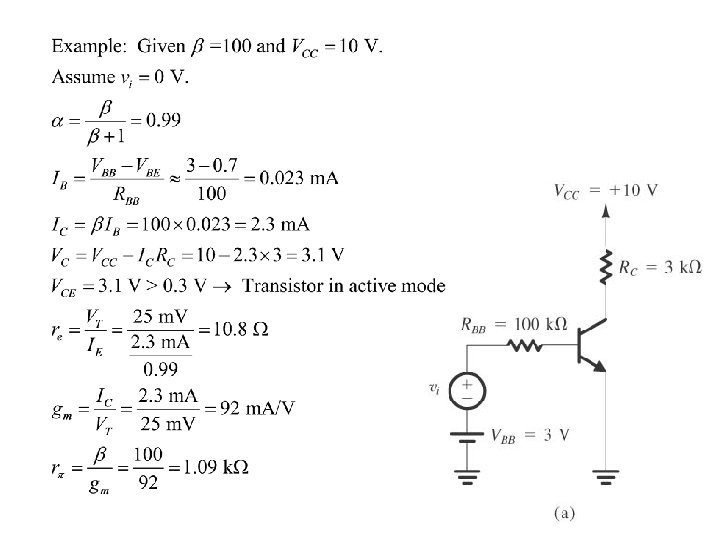
Biasing BJT • Determining a quiescent point for linearization • Active mode operation • Considerations – Stable with respect to manufacturing parameters (e. g. , ro, β) – Desired gains – Acceptable output swing

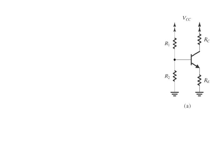
Biasing with Single Power Supply • Fix VBE or IB. • Output directly depends on β • Unstable with respect to temperature variation

Addition of Degeneration Resistor

Biasing with Two Power Supplies

Biasing with Feedback Resistor

Biasing with Current Source

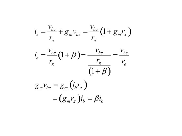
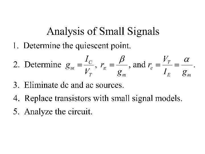
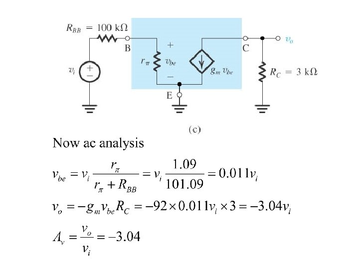
Small Signal Analysis • A quiescent point has been determined by biasing. • Active mode operation – Forward biasing for base-emitter junction by VBE – Reverse biasing for collector-base junction by RC and VCC
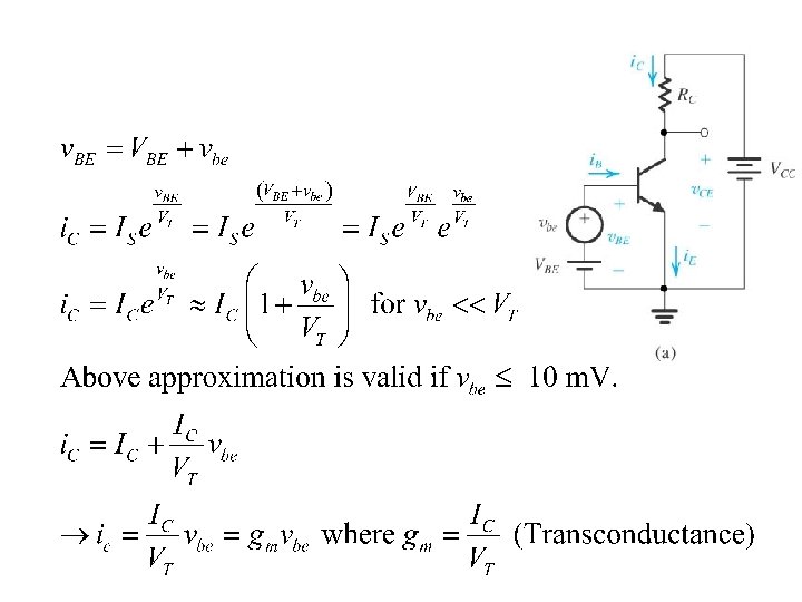

The transistor performs as a voltage controlled current source with gain gm when input varies by 10 m. V or less.
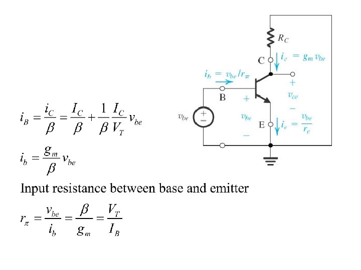


Hybrid π Model • Short circuit voltage sources • Open circuit current sources • Short circuit capacitors

T Model

Hybrid π Model with Early Effect

Structure of Single Stage Amplifier

Common Emitter Amplifier

Common Emitter Amplifier with RE

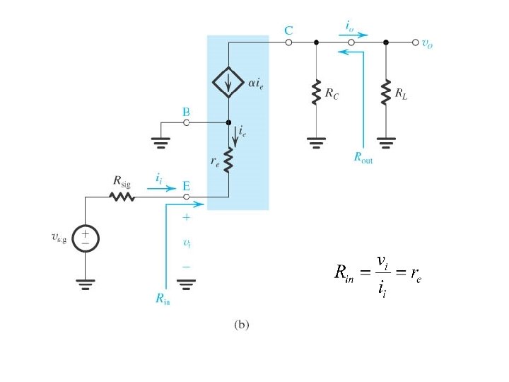
Common Base Amplifier


Common Collector Amplifier


Digital Logic Inverter Logic 1: v. I ≈ VCC → v. O =VCEsat ≈ 0. 2 V Logic 0: v. I ≈ 0 → v. O =VCC Transistor is in saturation mode.

v. I – v. O Transfer Function VCC = 5 V RB = 10 kΩ RC = 1 kΩ β = 50

- Slides: 71