Chapter 6 Basic radiation detectors Set of 60
Chapter 6: Basic radiation detectors Set of 60 slides based on the chapter authored by C. W. E. VAN EIJK Faculty of Applied Sciences, Delft University of Technology, Delft, Netherlands of the IAEA publication (ISBN 978– 92– 0– 143810– 2): Nuclear Medicine Physics: A Handbook for Teachers and Students Objective: To familiarize the student with the fundamental concepts of basic radiation detectors Slide set prepared in 2015 by J. Schwartz (New York, NY, USA) IAEA International Atomic Energy Agency
CHAPTER 6 6. 1. 6. 2. 6. 3. 6. 4. TABLE OF CONTENTS Introduction Gas filled detectors Semiconductor detectors Scintillation detectors and storage phosphors IAEA Nuclear Medicine Physics: A Handbook for Teachers and Students – Chapter 6 – Slide 2/60
6. 1. INTRODUCTION 6. 1. 1. Radiation detectors — complexity and relevance q Radiation detectors are of paramount importance in nuclear medicine q The detectors provide a wide range of information including: • Radiation dose of a laboratory worker • Positron emission tomography (PET) image of a patient q Consequently, detectors with strongly differing specifications are used IAEA Nuclear Medicine Physics: A Handbook for Teachers and Students – Chapter 6 – Slide 3/60

6. 1. INTRODUCTION 6. 1. 2. Interaction mechanisms, signal formation and detector type q Radiation detectors • Sensors that produce signals upon interaction with radiation • Signals can be processed electronically to give requested information q X-rays & -rays interaction mechanisms • • Photoelectric effect Compton scattering Pair production Relative importance depends on • Radiation energy • Interaction medium • Result in production of energetic electrons • These will eventually transfer their energy to interaction medium by ionization and excitation IAEA Nuclear Medicine Physics: A Handbook for Teachers and Students – Chapter 6 – Slide 4/60
6. 1. INTRODUCTION 6. 1. 2. Interaction mechanisms, signal formation and detector type q Charged particles transfer their energy by ionization & excitation q Ionization results in • Charge carriers production: ü Electrons and ions in a gaseous detection medium ü Electrons and holes in a semiconductor material ü Light quanta emission in scintillators q Radiation detectors • Charge or current forms signal • Signal created by charge motion in applied electric field ü Gas filled detectors ü Semiconductor detectors • Light emission observed using light sensor that produces charge or current ü Scintillation detectors IAEA Nuclear Medicine Physics: A Handbook for Teachers and Students – Chapter 6 – Slide 5/60
6. 1. INTRODUCTION 6. 1. 3. Counting, current, integrating mode q Radiology / radiotherapy radiation detectors • Operated in current mode • Intensities too high for individual counting of events q Nuclear medicine • Primarily use counting mode • Energy information • Arrival time information q Personal dosimeters • Detector used in integrating mode • Dose is measured monthly • Information extracted much later after actual interaction IAEA Nuclear Medicine Physics: A Handbook for Teachers and Students – Chapter 6 – Slide 6/60
6. 1. INTRODUCTION 6. 1. 4. Detector requirements q Radiation detector quality expressed in terms of • Sensitivity • Energy resolution • Time and position resolution • Counting rate performance IAEA Nuclear Medicine Physics: A Handbook for Teachers and Students – Chapter 6 – Slide 7/60
6. 1. INTRODUCTION 6. 1. 4. Detector requirements 6. 1. 4. 1. Sensitivity q Sensitivity depends on • Subtended solid angle • Detector efficiency for radiation interaction • Relevant energy range is ~30– 511 ke. V, where it’s governed by: • Photoelectric effect • Attenuation length (cm) ~ ρZeff 3– 4 ρ = density, Zeff = effective atomic number of the compound • Compton scattering • Almost independent of Z • Proportional to ρ • ρ of gas-filled detector is 3 orders of magnitude smaller than for solid state detector • Need highest possible ρ and Zeff at 511 ke. V IAEA Nuclear Medicine Physics: A Handbook for Teachers and Students – Chapter 6 – Slide 8/60
6. 1. INTRODUCTION 6. 1. 4. Detector requirements 6. 1. 4. 2. Energy, time and position resolution q Energy resolution • Strongly coupled to number of information carriers • Number of information carriers • Given by N = E/W • E = Radiation energy • W = Mean energy needed to produce information carrier • Largest number produced in semiconductors • Smallest number produced in inorganic scintillators + PMT’s IAEA Nuclear Medicine Physics: A Handbook for Teachers and Students – Chapter 6 – Slide 9/60
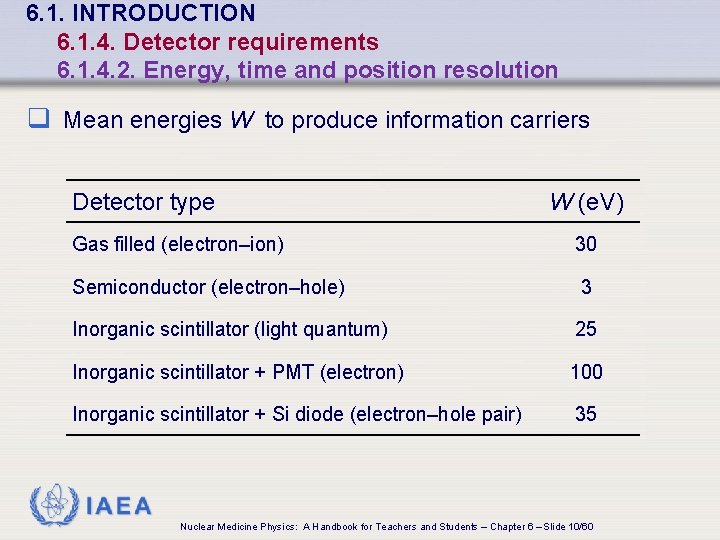
6. 1. INTRODUCTION 6. 1. 4. Detector requirements 6. 1. 4. 2. Energy, time and position resolution q Mean energies W to produce information carriers Detector type W (e. V) Gas filled (electron–ion) 30 Semiconductor (electron–hole) 3 Inorganic scintillator (light quantum) 25 Inorganic scintillator + PMT (electron) 100 Inorganic scintillator + Si diode (electron–hole pair) 35 IAEA Nuclear Medicine Physics: A Handbook for Teachers and Students – Chapter 6 – Slide 10/60
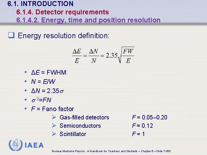
6. 1. INTRODUCTION 6. 1. 4. Detector requirements 6. 1. 4. 2. Energy, time and position resolution q Energy resolution definition: • • • ΔE = FWHM N = E/W ΔN = 2. 35 2=FN F = Fano factor Ø Gas-filled detectors Ø Semiconductors Ø Scintillator F = 0. 05– 0. 20 F ≈ 0. 12 F=1 IAEA Nuclear Medicine Physics: A Handbook for Teachers and Students – Chapter 6 – Slide 11/60
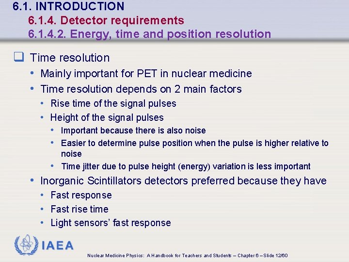
6. 1. INTRODUCTION 6. 1. 4. Detector requirements 6. 1. 4. 2. Energy, time and position resolution q Time resolution • Mainly important for PET in nuclear medicine • Time resolution depends on 2 main factors • Rise time of the signal pulses • Height of the signal pulses • Important because there is also noise • Easier to determine pulse position when the pulse is higher relative to noise • Time jitter due to pulse height (energy) variation is less important • Inorganic Scintillators detectors preferred because they have • Fast response • Fast rise time • Light sensors’ fast response IAEA Nuclear Medicine Physics: A Handbook for Teachers and Students – Chapter 6 – Slide 12/60
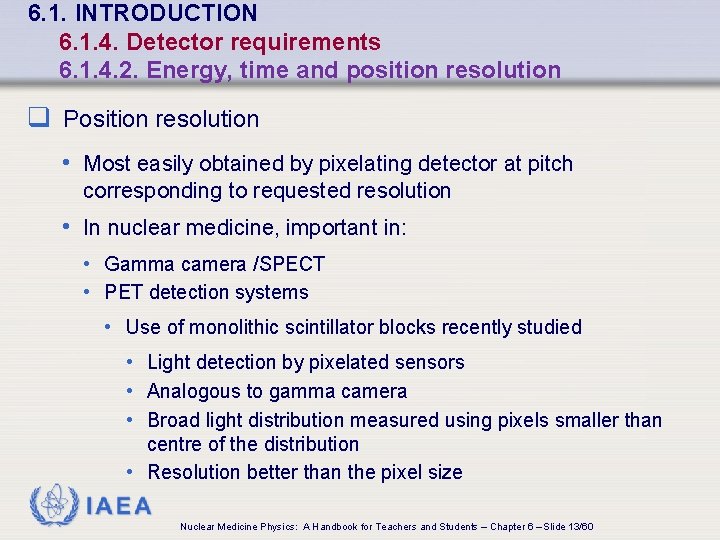
6. 1. INTRODUCTION 6. 1. 4. Detector requirements 6. 1. 4. 2. Energy, time and position resolution q Position resolution • Most easily obtained by pixelating detector at pitch corresponding to requested resolution • In nuclear medicine, important in: • Gamma camera /SPECT • PET detection systems • Use of monolithic scintillator blocks recently studied • Light detection by pixelated sensors • Analogous to gamma camera • Broad light distribution measured using pixels smaller than centre of the distribution • Resolution better than the pixel size IAEA Nuclear Medicine Physics: A Handbook for Teachers and Students – Chapter 6 – Slide 13/60
6. 1. INTRODUCTION 6. 1. 4. Detector requirements 6. 1. 4. 3. Counting rate and dead time q Achievable counting rate depends on • Detector response time • Time to transport charge carriers to form signal • Time to emit the scintillation light • Time needed to process the signals • Time needed to handle the data IAEA Nuclear Medicine Physics: A Handbook for Teachers and Students – Chapter 6 – Slide 14/60
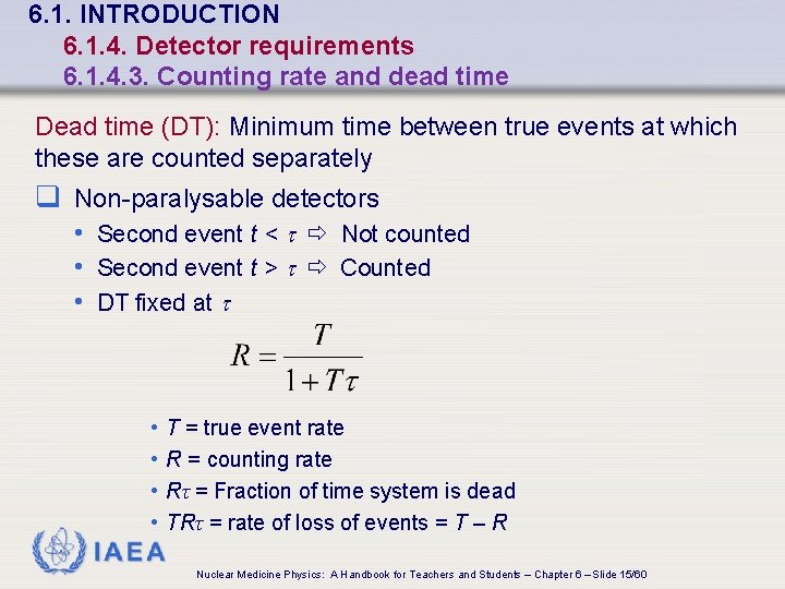
6. 1. INTRODUCTION 6. 1. 4. Detector requirements 6. 1. 4. 3. Counting rate and dead time Dead time (DT): Minimum time between true events at which these are counted separately q Non-paralysable detectors • Second event t < t Not counted • Second event t > t Counted • DT fixed at t • T = true event rate • R = counting rate • Rτ = Fraction of time system is dead • TRτ = rate of loss of events = T – R IAEA Nuclear Medicine Physics: A Handbook for Teachers and Students – Chapter 6 – Slide 15/60
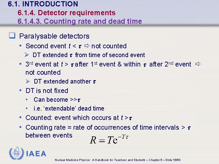
6. 1. INTRODUCTION 6. 1. 4. Detector requirements 6. 1. 4. 3. Counting rate and dead time q Paralysable detectors • Second event t < t not counted Ø DT extended t from time of second event • 3 rd event at t > t after 1 st event & within t after 2 nd event not counted Ø DT extended another t • DT is not fixed • Can become >>t • i. e. ‘extendable’ dead time • Counted: event which occurs at t >t • Counting rate = rate of occurrences of time intervals > t between events IAEA Nuclear Medicine Physics: A Handbook for Teachers and Students – Chapter 6 – Slide 16/60
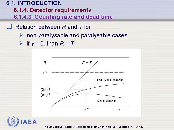
6. 1. INTRODUCTION 6. 1. 4. Detector requirements 6. 1. 4. 3. Counting rate and dead time q Relation between R and T for Ø non-paralysable and paralysable cases Ø if t = 0, than R = T IAEA Nuclear Medicine Physics: A Handbook for Teachers and Students – Chapter 6 – Slide 17/60
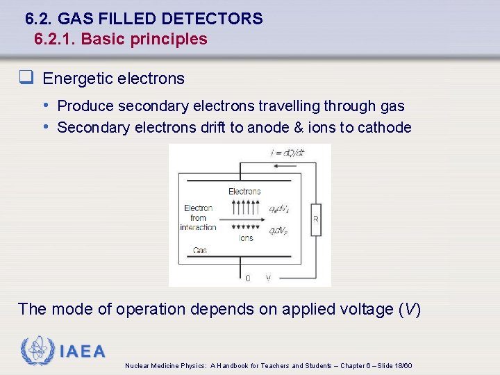
6. 2. GAS FILLED DETECTORS 6. 2. 1. Basic principles q Energetic electrons • Produce secondary electrons travelling through gas • Secondary electrons drift to anode & ions to cathode The mode of operation depends on applied voltage (V) IAEA Nuclear Medicine Physics: A Handbook for Teachers and Students – Chapter 6 – Slide 18/60
6. 2. GAS FILLED DETECTORS 6. 2. 1. Basic principles Ø Relatively low V • • • Recombination region Produces weak electric field E E too weak to efficiently separate the (-) and (+) charges Some will recombine Full signal not observed Increasing V decreases recombination Ø Relatively high voltage V • • Full ionization Heavier charged particles & higher rates higher V Signal becomes constant over wide V range Typical operating V of ionization chamber: 500 to 1000 V IAEA Nuclear Medicine Physics: A Handbook for Teachers and Students – Chapter 6 – Slide 19/60
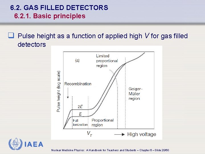
6. 2. GAS FILLED DETECTORS 6. 2. 1. Basic principles q Pulse height as a function of applied high V for gas filled detectors IAEA Nuclear Medicine Physics: A Handbook for Teachers and Students – Chapter 6 – Slide 20/60
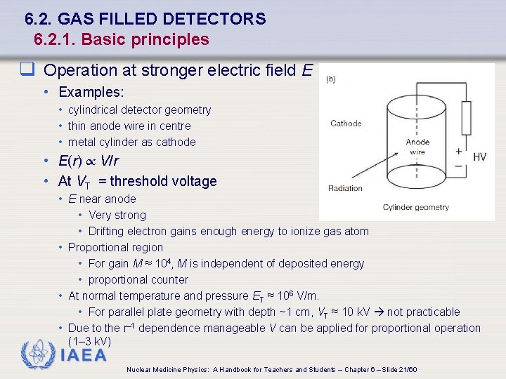
6. 2. GAS FILLED DETECTORS 6. 2. 1. Basic principles q Operation at stronger electric field E • Examples: • cylindrical detector geometry • thin anode wire in centre • metal cylinder as cathode • E(r) V/r • At VT = threshold voltage • E near anode • Very strong • Drifting electron gains enough energy to ionize gas atom • Proportional region • For gain M ≈ 104, M is independent of deposited energy • proportional counter • At normal temperature and pressure ET ≈ 106 V/m. • For parallel plate geometry with depth ~1 cm, VT ≈ 10 k. V not practicable • Due to the r– 1 dependence manageable V can be applied for proportional operation (1– 3 k. V) IAEA Nuclear Medicine Physics: A Handbook for Teachers and Students – Chapter 6 – Slide 21/60
6. 2. GAS FILLED DETECTORS 6. 2. 1. Basic principles q Operation at stronger electric field E • At further increased V • Space charge effects start to reduce effective E • Affect the gain • Process will start at lower V for higher primary ionization density events • Limited proportionality region is entered • At further increased V • Pulse height will become independent of the deposited energy • Geiger–Müller region is entered • V further increased • Ionization zone expands • Avalanche & significant amplification obtained IAEA Nuclear Medicine Physics: A Handbook for Teachers and Students – Chapter 6 – Slide 22/60
6. 2. GAS FILLED DETECTORS 6. 2. 1. Basic principles q Multi-wire proportional chamber (MWPC) • Alternate geometry • Many equidistant parallel anode wires • Pitch of 1– 2 mm • Positioned in a plane inside a box • Walls are cathode planes • Employed in autoradiography • Micro-patterned detectors made with photo-lithography • Operate analogously to the MWPC • Examples: • Micro-strip gas chamber • Gas electron multiplier • Spatial resolutions are of the order of 0. 1 mm IAEA Nuclear Medicine Physics: A Handbook for Teachers and Students – Chapter 6 – Slide 23/60
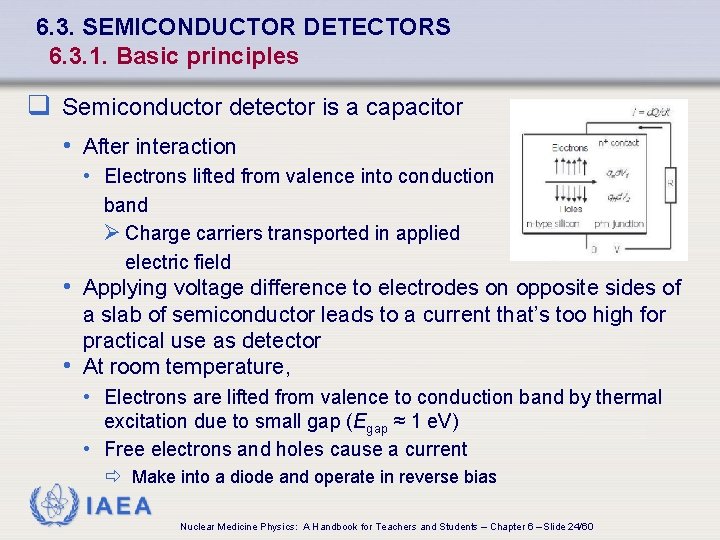
6. 3. SEMICONDUCTOR DETECTORS 6. 3. 1. Basic principles q Semiconductor detector is a capacitor • After interaction • Electrons lifted from valence into conduction band Ø Charge carriers transported in applied electric field • Applying voltage difference to electrodes on opposite sides of a slab of semiconductor leads to a current that’s too high for practical use as detector • At room temperature, • Electrons are lifted from valence to conduction band by thermal excitation due to small gap (Egap ≈ 1 e. V) • Free electrons and holes cause a current Make into a diode and operate in reverse bias IAEA Nuclear Medicine Physics: A Handbook for Teachers and Students – Chapter 6 – Slide 24/60
6. 3. SEMICONDUCTOR DETECTORS 6. 3. 1. Basic principles q Example: Silicon • Semiconductor-electronics used to make diode structure • N-type silicon • Doped with electron-donor impurities • Reduces number of holes • Electrons are the majority charge carriers • P-type silicon • Doped with electron-acceptor impurities • Strongly reduces number of free electrons • Holes are the majority charge carriers IAEA Nuclear Medicine Physics: A Handbook for Teachers and Students – Chapter 6 – Slide 25/60
6. 3. SEMICONDUCTOR DETECTORS 6. 3. 1. Basic principles q Example: Silicon • Junction diode • Formed when n-type brought into contact with p-type material • Depletion region • Space charge zone results at junction • Due to diffusion of majority charge carriers • Reverse-biased • Positive voltage applied on n-type side with respect to p-type side • Depletion layer thickness increased • High enough voltage fully depletes layer • No free charge carriers left • Virtually no current flows • Only small current remains (leakage or dark current) IAEA Nuclear Medicine Physics: A Handbook for Teachers and Students – Chapter 6 – Slide 26/60
6. 3. SEMICONDUCTOR DETECTORS 6. 3. 1. Basic principles q Example: Silicon • Diode • n-type doped with impurities in narrow zone • makes p+ n junction • p+: high doping concentration • Use high-purity Si & blocking contact for further leakage current reduction • n+ doping at n-type side • If the leakage current is still problematic, the temperature can be decreased • Use of high purity semiconductor material is important for reducing leakage current • Energy levels in the gap may trap charge carriers resulting from the interaction with radiation and the energy resolution of a detector would be reduced IAEA Nuclear Medicine Physics: A Handbook for Teachers and Students – Chapter 6 – Slide 27/60
6. 3. SEMICONDUCTOR DETECTORS 6. 3. 1. Basic principles q Example: Silicon Other approaches to make a detector • Start with p-type material and make n+p junction diode • Apply a combination of surface oxidation and deposition of thin metal layer • Called surface barrier contacts • For thicknesses <1 mm it’s possible to use intrinsic Si with p+ & n+ blocking contacts on opposite sides (p–i–n configuration) • For thicker detectors impurities are compensated for by introducing interstitial Li ions • Use slightly p-type intrinsic Si • Li ions act as electron donors • Li ions can be drifted 10 mm • For large enough band gap metal contacts will suffice IAEA Nuclear Medicine Physics: A Handbook for Teachers and Students – Chapter 6 – Slide 28/60
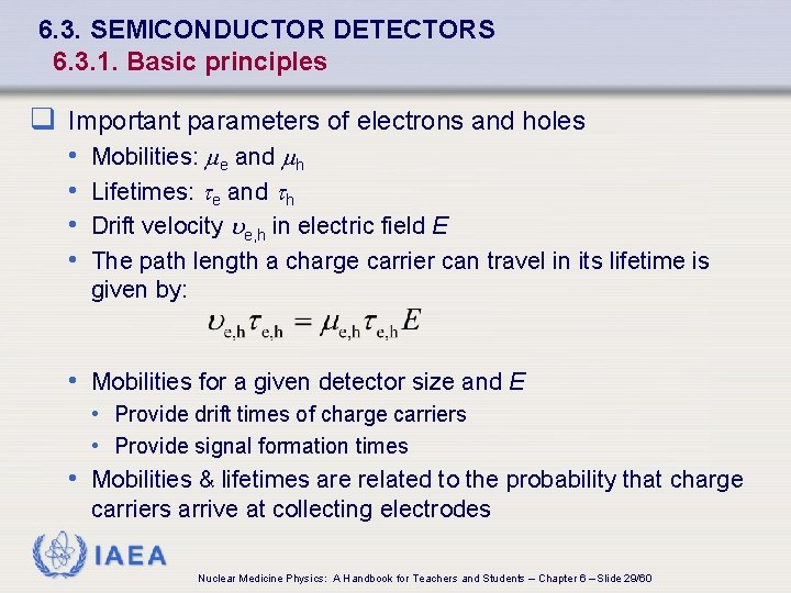
6. 3. SEMICONDUCTOR DETECTORS 6. 3. 1. Basic principles q Important parameters of electrons and holes • • Mobilities: me and mh Lifetimes: te and th Drift velocity e, h in electric field E The path length a charge carrier can travel in its lifetime is given by: • Mobilities for a given detector size and E • Provide drift times of charge carriers • Provide signal formation times • Mobilities & lifetimes are related to the probability that charge carriers arrive at collecting electrodes IAEA Nuclear Medicine Physics: A Handbook for Teachers and Students – Chapter 6 – Slide 29/60
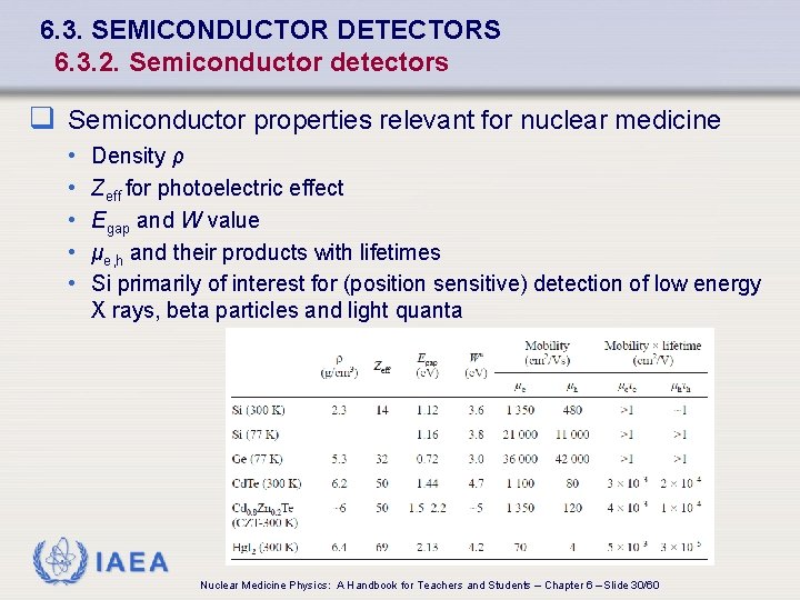
6. 3. SEMICONDUCTOR DETECTORS 6. 3. 2. Semiconductor detectors q Semiconductor properties relevant for nuclear medicine • • • Density ρ Zeff for photoelectric effect Egap and W value μe, h and their products with lifetimes Si primarily of interest for (position sensitive) detection of low energy X rays, beta particles and light quanta IAEA Nuclear Medicine Physics: A Handbook for Teachers and Students – Chapter 6 – Slide 30/60
6. 3. SEMICONDUCTOR DETECTORS 6. 3. 2. Semiconductor detectors q Detection of X-rays of 300 e. V - 60 ke. V • Si(Li) • • Commercially available planar circular Li drifted p–i–n Thickness up to 5 mm Diameters 4– 20 mm For typical E=1000 V/cm drift times to electrodes are on the order of tens of ns • Energy resolutions (FWHM) at 5. 9 ke. V are 130– 220 e. V at 77 K • Position sensitive Si detectors commercially available with a large variety of pixel structures • Si detectors also used in personal dosimeters IAEA Nuclear Medicine Physics: A Handbook for Teachers and Students – Chapter 6 – Slide 31/60
6. 3. SEMICONDUCTOR DETECTORS 6. 3. 2. Semiconductor detectors q High resolution gamma-ray spectroscopy uses Ge detectors • Higher density & Z • Made of high purity material • Large volume detectors in coaxial geometry • Made of cylindrical crystals with core removed • High purity n-type or p-type used with corresponding junction • Contacts on outside and blocking contacts on inside • Operated at 77 K • Commercially available cylindrical detectors • Diameter ≤ 10 cm, height ≤ 10 cm • Drift times to electrodes ≤ 100 ns • Typical energy resolutions • 1 ke. V at 122 ke. V -ray energy • 2 ke. V at 1332 ke. V -ray energy IAEA Nuclear Medicine Physics: A Handbook for Teachers and Students – Chapter 6 – Slide 32/60
6. 3. SEMICONDUCTOR DETECTORS 6. 3. 2. Semiconductor detectors q Cd. Te (cadmium telluride) and CZT (cadmium zinc telluride) • • Z is significantly higher than for Ge Possible to operate at room temperature due to larger band gap High purity n-type or p-type material is used Worse energy resolution than Ge • e. g. 2. 5% FWHM at 662 ke. V (primarily due to relatively short lifetime of holes, resulting in incomplete charge collection) • To observe the electron signal only use either or both: • Electronic correction techniques • Detectors with special electrode configurations (small pixels or grids) • Dimensions: ~ 25 × 10 mm 3 • 16 × 16 pixels detectors are available • e. g. used for SPECT innovation IAEA Nuclear Medicine Physics: A Handbook for Teachers and Students – Chapter 6 – Slide 33/60
6. 3. SEMICONDUCTOR DETECTORS 6. 3. 2. Semiconductor detectors q Hg. I 2 (mercury iodide) is attractive for efficient -ray detection • Large density and high Z • Room temperature operation possible due large band gap • Cons • Mobilities are low • Charge collection, in particular of holes, is poor • Application is limited to thicknesses ≤ 10 mm • E = 2500 V/cm • Areas 30 x 30 mm 2 IAEA Nuclear Medicine Physics: A Handbook for Teachers and Students – Chapter 6 – Slide 34/60
6. 4. SCINTILLATION DETECTORS AND STORAGE PHOSPHORS 6. 4. 1. Basic principles q Scintillation is prompt emission of light after radiation interaction q In nuclear medicine, inorganic ionic crystals are most important • • • High density & Z Fast response High light yield Large crystals can be grown Primarily for X-ray and -ray detection Metastable states (traps) are created in some materials • may live ms to months (storage phosphors) q Organic scintillators are another group • Crystals, plastics and liquids • Low density & Z • Primarily for counting β particles IAEA Nuclear Medicine Physics: A Handbook for Teachers and Students – Chapter 6 – Slide 35/60
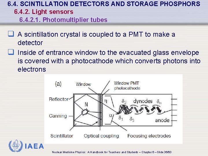
6. 4. SCINTILLATION DETECTORS AND STORAGE PHOSPHORS 6. 4. 2. Light sensors 6. 4. 2. 1. Photomultiplier tubes q A scintillation crystal is coupled to a PMT to make a detector q Inside of entrance window to the evacuated glass envelope is covered with a photocathode which converts photons into electrons IAEA Nuclear Medicine Physics: A Handbook for Teachers and Students – Chapter 6 – Slide 36/60
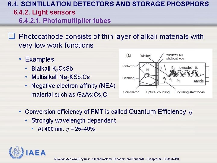
6. 4. SCINTILLATION DETECTORS AND STORAGE PHOSPHORS 6. 4. 2. Light sensors 6. 4. 2. 1. Photomultiplier tubes q Photocathode consists of thin layer of alkali materials with very low work functions • Examples • Bialkali K 2 Cs. Sb • Multialkali Na 2 KSb: Cs • Negative electron affinity (NEA) material such as Ga. As: Cs, O • Conversion efficiency of PMT is called Quantum Efficiency h • Strongly wavelength dependent • At 400 nm, h = 25– 40% IAEA Nuclear Medicine Physics: A Handbook for Teachers and Students – Chapter 6 – Slide 37/60
6. 4. SCINTILLATION DETECTORS AND STORAGE PHOSPHORS 6. 4. 2. Light sensors 6. 4. 2. 1. Photomultiplier tubes q Emitted electrons focused onto first dynode via electrode structure • Applied voltage = 200– 500 V • Collection efficiency a ≈ 95% • Typical materials are Be. O–Cu, Cs 3 Sb and Ga. P: Cs • • • The latter is an NEA material Electrons released by secondary emission if electron hits dynode • Focused onto next dynode • Secondary electrons emitted again N = Number of dynodes = 8– 12 Last dynode (anode) provides signal Multiplication factor • d ≈ 5 per dynode at inter-dynode voltage = 100 V • First dynode has higher multiplication factor d 1≥ 10 • Improves single-electron pulse resolution & signal to noise ratio IAEA Nuclear Medicine Physics: A Handbook for Teachers and Students – Chapter 6 – Slide 38/60
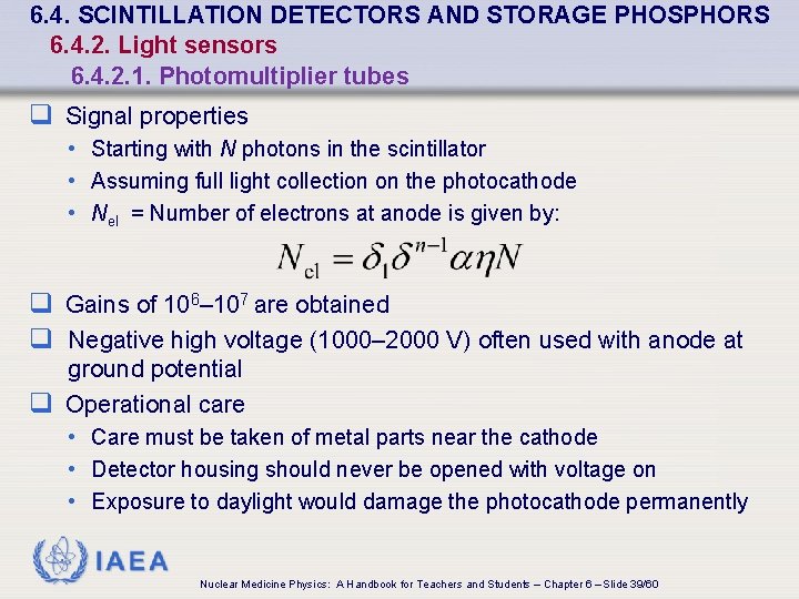
6. 4. SCINTILLATION DETECTORS AND STORAGE PHOSPHORS 6. 4. 2. Light sensors 6. 4. 2. 1. Photomultiplier tubes q Signal properties • Starting with N photons in the scintillator • Assuming full light collection on the photocathode • Nel = Number of electrons at anode is given by: q Gains of 106– 107 are obtained q Negative high voltage (1000– 2000 V) often used with anode at ground potential q Operational care • Care must be taken of metal parts near the cathode • Detector housing should never be opened with voltage on • Exposure to daylight would damage the photocathode permanently IAEA Nuclear Medicine Physics: A Handbook for Teachers and Students – Chapter 6 – Slide 39/60

6. 4. SCINTILLATION DETECTORS AND STORAGE PHOSPHORS 6. 4. 2. Light sensors 6. 4. 2. 1. Photomultiplier tubes q PMTs • • Available with circular, square or hexagonal photocathodes Cathode diameters = 10 - 150 mm If diameter ~ 50 mm length ~ 150 mm (including contact pins) Also available pixelated with multi-anode q Time resolution optimized by making special tubes with electron transit times as the anode, independent of cathode position where electron emitted q Electron transit time ~ 30 ns q Spread standard deviation ~ 250 ps q Signal rise time ~ 1. 5 ns IAEA Nuclear Medicine Physics: A Handbook for Teachers and Students – Chapter 6 – Slide 40/60
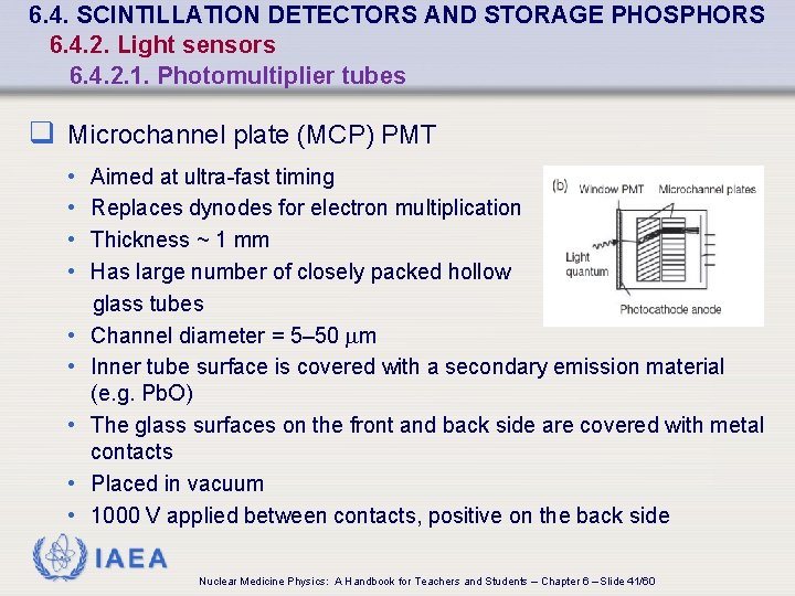
6. 4. SCINTILLATION DETECTORS AND STORAGE PHOSPHORS 6. 4. 2. Light sensors 6. 4. 2. 1. Photomultiplier tubes q Microchannel plate (MCP) PMT • • • Aimed at ultra-fast timing Replaces dynodes for electron multiplication Thickness ~ 1 mm Has large number of closely packed hollow glass tubes Channel diameter = 5– 50 mm Inner tube surface is covered with a secondary emission material (e. g. Pb. O) The glass surfaces on the front and back side are covered with metal contacts Placed in vacuum 1000 V applied between contacts, positive on the back side IAEA Nuclear Medicine Physics: A Handbook for Teachers and Students – Chapter 6 – Slide 41/60
6. 4. SCINTILLATION DETECTORS AND STORAGE PHOSPHORS 6. 4. 2. Light sensors 6. 4. 2. 1. Photomultiplier tubes q Microchannel plate (MCP) • An electron enters glass tube on front side & hits wall • Secondary electron emission occurs • Electrons pulled to back side by E • Hit channel wall & produce secondaries, etc. • Eventually leave tube at back • Electron multiplication ≤ 104 IAEA Nuclear Medicine Physics: A Handbook for Teachers and Students – Chapter 6 – Slide 42/60
6. 4. SCINTILLATION DETECTORS AND STORAGE PHOSPHORS 6. 4. 2. Light sensors 6. 4. 2. 1. Photomultiplier tubes q MCP-PMT uses 2 MCPs at close distance • Structure called chevron • Glass tubes at an angle • Prevent ions from gaining too much energy • At 3000 V, stable gains ~ 106 • Advantage: short path length of electrons • Transit times ~ few ns • Transit time spreads ~ 100 ps • Commercially available as: • Circular with diameter = 10 mm • Square with multi-anode structures • Sensitive between 115 nm (Mg. F 2 window) - infrared IAEA Nuclear Medicine Physics: A Handbook for Teachers and Students – Chapter 6 – Slide 43/60
6. 4. SCINTILLATION DETECTORS AND STORAGE PHOSPHORS 6. 4. 2. Light sensors 6. 4. 2. 2. Silicon based photon sensors q Si photodiodes preferred in some applications • PMTs have large size, high voltages, small quantum efficiency and sensitivity to magnetic fields • Si diodes are usually p–i–n structure (PIN diodes) • Thickness = 2 mm including packaging • Shapes: circular, rectangular or square, up to 30 mm × 30 mm • Bias voltages < 150 V IAEA Nuclear Medicine Physics: A Handbook for Teachers and Students – Chapter 6 – Slide 44/60
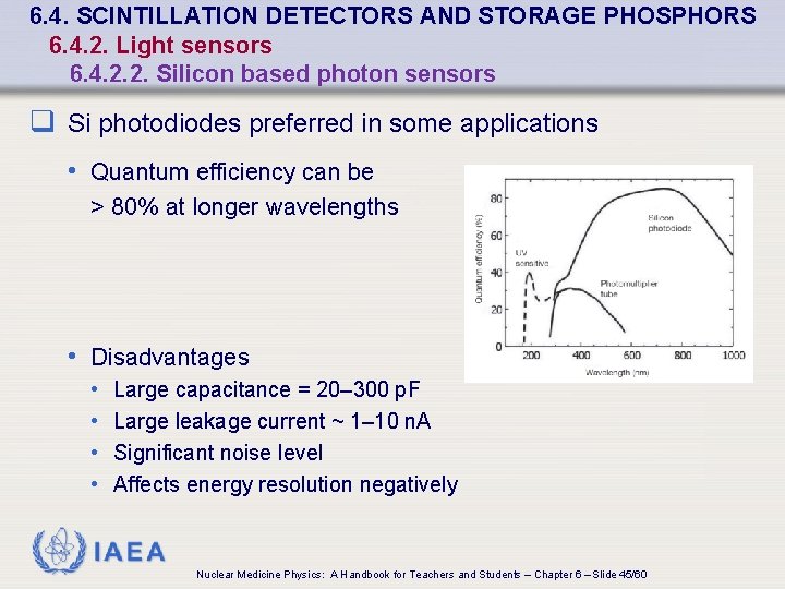
6. 4. SCINTILLATION DETECTORS AND STORAGE PHOSPHORS 6. 4. 2. Light sensors 6. 4. 2. 2. Silicon based photon sensors q Si photodiodes preferred in some applications • Quantum efficiency can be > 80% at longer wavelengths • Disadvantages • • Large capacitance = 20– 300 p. F Large leakage current ~ 1– 10 n. A Significant noise level Affects energy resolution negatively IAEA Nuclear Medicine Physics: A Handbook for Teachers and Students – Chapter 6 – Slide 45/60
6. 4. SCINTILLATION DETECTORS AND STORAGE PHOSPHORS 6. 4. 2. Light sensors 6. 4. 2. 2. Silicon based photon sensors q Avalanche photodiode (APD) • Semiconductor analogue to proportional counter • A high E-field is created in small zone • Drifting electron can gain enough energy to produce (e–h) pair • An avalanche results • Critical field for multiplication = 107 V/m • Higher V higher gain • Voltages applied = 50– 1500 V depending on type • Gains are M 1000 • Lifts signal well above noise as compared to Si diode • At a certain gain, the advantage is optimal IAEA Nuclear Medicine Physics: A Handbook for Teachers and Students – Chapter 6 – Slide 46/60
6. 4. SCINTILLATION DETECTORS AND STORAGE PHOSPHORS 6. 4. 2. Light sensors 6. 4. 2. 2. Silicon based photon sensors q Avalanche photodiode (APD) • Break-down voltage Vbr • Spontaneous charge multiplication occurs • At voltages > Vbr • • For gains of M 105 – 106 Geiger mode Pulses are equal in magnitude Signal quenching techniques have to be used • Available as circular & square with areas = sub-mm 2 -1 cm 2 • Available with various pixelations • e. g. of 4 × 8 at 2. 5 mm pitch & fill factor ≤ 40% IAEA Nuclear Medicine Physics: A Handbook for Teachers and Students – Chapter 6 – Slide 47/60
6. 4. SCINTILLATION DETECTORS AND STORAGE PHOSPHORS 6. 4. 2. Light sensors 6. 4. 2. 2. Silicon based photon sensors q Hybrid photomultiplier tube (HPMT) • • Voltage between photocathode & Si diode ~ 10 k. V Si diode placed inside vacuum enclosure Photoelectrons accelerated in resulting E field Diode is relatively small • Reduces capacitance which reduces noise level • Need 3. 6 e. V to produce 1 e–h pair • 3000 e–h pairs produced per impinging electron • Signals from one or more photons are well separated • Possible overall gain with APD = 105 • Window diameters are as large as 70 mm IAEA Nuclear Medicine Physics: A Handbook for Teachers and Students – Chapter 6 – Slide 48/60
6. 4. SCINTILLATION DETECTORS AND STORAGE PHOSPHORS 6. 4. 2. Light sensors 6. 4. 2. 2. Silicon based photon sensors q Silicon photomultiplier (Si. PM) • Array of tiny APDs operating in Geiger mode • Dimensions: 20 × 20 μm 2 to 100 × 100 μm 2 • Number of APDs per mm 2 = 2500 – 100 • Fill factor from < 30% to 80% for smallest to largest dimensions • All APDs signals are summed • Time spread < 100 ps • Excellent time resolutions IAEA Nuclear Medicine Physics: A Handbook for Teachers and Students – Chapter 6 – Slide 49/60
6. 4. SCINTILLATION DETECTORS AND STORAGE PHOSPHORS 6. 4. 2. Light sensors 6. 4. 2. 2. Silicon based photon sensors q Silicon photomultiplier (Si. PM) • Gains M = 105– 106 • Can easily obtain a signal from a single photon • Spontaneous Geiger pulses can be eliminated by setting a threshold above the one electron response • Available arrays • • • 2 × 2 pixels and 4 × 4 pixels 3 × 3 mm 2 each Pitch of 4 mm A 16 × 16 pixel array of 50 × 50 mm 2 (recently introduced) Blue sensitive Si. PMs have detection efficiency of 25% at 400 nm, including a 60% fill factor IAEA Nuclear Medicine Physics: A Handbook for Teachers and Students – Chapter 6 – Slide 50/60
6. 4. SCINTILLATION DETECTORS AND STORAGE PHOSPHORS 6. 4. 3. Scintillator materials 6. 4. 3. 1. Inorganic scintillators q Inorganic scintillator bandgap has to be relatively large so as to: • Egap ≥ 4 e. V • Avoid thermal excitation • Allow scintillation photons to travel in material without absorption q Thus: inorganic scintillators are based on ionic-crystal materials IAEA Nuclear Medicine Physics: A Handbook for Teachers and Students – Chapter 6 – Slide 51/60
6. 4. SCINTILLATION DETECTORS AND STORAGE PHOSPHORS 6. 4. 3. Scintillator materials 6. 4. 3. 1. Inorganic scintillators q Three steps scintillation photons production 1. Interaction with bulk material & thermalization of electrons and holes • Electrons go to bottom of conduction band • Holes go to top of the valence band 2. Transport of charge carriers to intrinsic or dopant luminescence centres 3. Interaction with these centres • Excitation • Relaxation • Scintillation IAEA Nuclear Medicine Physics: A Handbook for Teachers and Students – Chapter 6 – Slide 52/60
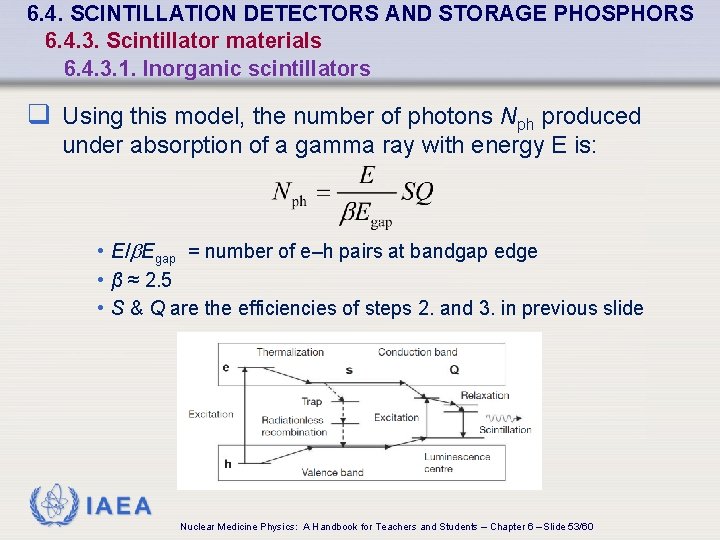
6. 4. SCINTILLATION DETECTORS AND STORAGE PHOSPHORS 6. 4. 3. Scintillator materials 6. 4. 3. 1. Inorganic scintillators q Using this model, the number of photons Nph produced under absorption of a gamma ray with energy E is: • E/b. Egap = number of e–h pairs at bandgap edge • β ≈ 2. 5 • S & Q are the efficiencies of steps 2. and 3. in previous slide IAEA Nuclear Medicine Physics: A Handbook for Teachers and Students – Chapter 6 – Slide 53/60
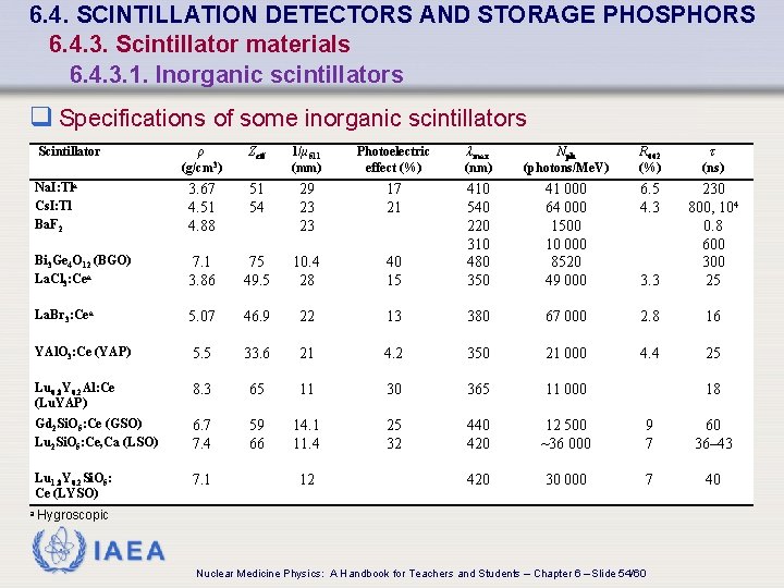
6. 4. SCINTILLATION DETECTORS AND STORAGE PHOSPHORS 6. 4. 3. Scintillator materials 6. 4. 3. 1. Inorganic scintillators q Specifications of some inorganic scintillators Scintillator a ρ (g/cm 3) Zeff 1/μ 511 (mm) Photoelectric effect (%) λmax (nm) Nph (photons/Me. V) R 662 (%) τ (ns) Na. I: Tla Cs. I: Tl Ba. F 2 3. 67 4. 51 4. 88 51 54 29 23 23 17 21 7. 1 3. 86 75 49. 5 10. 4 28 40 15 41 000 64 000 1500 10 000 8520 49 000 6. 5 4. 3 Bi 3 Ge 4 O 12 (BGO) La. Cl 3: Cea 410 540 220 310 480 350 3. 3 230 800, 104 0. 8 600 300 25 La. Br 3: Cea 5. 07 46. 9 22 13 380 67 000 2. 8 16 YAl. O 3: Ce (YAP) 5. 5 33. 6 21 4. 2 350 21 000 4. 4 25 Lu 0. 8 Y 0. 2 Al: Ce (Lu. YAP) 8. 3 65 11 30 365 11 000 Gd 2 Si. O 5: Ce (GSO) Lu 2 Si. O 5: Ce, Ca (LSO) 6. 7 7. 4 59 66 14. 1 11. 4 25 32 440 420 12 500 ~36 000 9 7 60 36– 43 Lu 1. 8 Y 0. 2 Si. O 5: Ce (LYSO) 7. 1 420 30 000 7 40 12 Hygroscopic IAEA Nuclear Medicine Physics: A Handbook for Teachers and Students – Chapter 6 – Slide 54/60 18
6. 4. SCINTILLATION DETECTORS AND STORAGE PHOSPHORS 6. 4. 3. Scintillator materials 6. 4. 3. 1. Inorganic scintillators q The scintillators in the table are commercially available q If hygroscopic, they are canned with reflective material q Only Ba. F 2 and BGO have intrinsic luminescence centre q Others have Tl+ or Ce 3+ ions as dopant luminescence centre • Ce doped scintillators show a relatively fast response • Of the order of tens of ns • Due to allowed 5 d → 4 f dipole transition of the Ce ion • Tl doped scintillators much slower because these transitions are forbidden IAEA Nuclear Medicine Physics: A Handbook for Teachers and Students – Chapter 6 – Slide 55/60
6. 4. SCINTILLATION DETECTORS AND STORAGE PHOSPHORS 6. 4. 3. Scintillator materials 6. 4. 3. 1. Inorganic scintillators q In general, mixed or co-doped crystals have advantages in: • Crystal growing • Response time • Light yield • Large variation due to S < 1 • Afterglow effects IAEA Nuclear Medicine Physics: A Handbook for Teachers and Students – Chapter 6 – Slide 56/60
6. 4. SCINTILLATION DETECTORS AND STORAGE PHOSPHORS 6. 4. 3. Scintillator materials 6. 4. 3. 2. Organic scintillators — crystals, plastics and liquids q Organic scintillators scintillation mechanism based on molecular transitions • Hardly affected by physical state of the material q There are pure organic scintillator crystals such as • Anthracene • Plastics • Polystyrene • Liquids (Xylene) IAEA Nuclear Medicine Physics: A Handbook for Teachers and Students – Chapter 6 – Slide 57/60
6. 4. SCINTILLATION DETECTORS AND STORAGE PHOSPHORS 6. 4. 3. Scintillator materials 6. 4. 3. 2. Organic scintillators — crystals, plastics and liquids q There also solutions of organic scintillators in organic solid (plastic) and liquid solvents • Typical combinations: p-terphenyl in polysterene (plastic) and p-terphenyl in toluene q There also systems with POPOP added for wavelength shifting. In general: • Organic scintillators luminesce at ~420 nm, have a light yield of ~10 000 photons/Me. V of absorbed -ray energy • Decay times are about 2 ns IAEA Nuclear Medicine Physics: A Handbook for Teachers and Students – Chapter 6 – Slide 58/60
6. 4. SCINTILLATION DETECTORS AND STORAGE PHOSPHORS 6. 4. 3. Scintillator materials 6. 4. 3. 3. Storage phosphors — thermoluminescence /optically stimulated luminescence q Storage phosphor • Analogous to inorganic scintillator • Difference: a significant part of interaction energy is stored in long-living traps • These are the memory bits of a storage phosphor • The lifetime must be long enough for the application considered q Readout is done by thermal (heating) or optical stimulation • Electron lifted from the trap into the conduction band transported to a luminescence centre • The intensity of the luminescence is recorded • Processes called thermoluminescence & optically/photon stimulated luminescence IAEA Nuclear Medicine Physics: A Handbook for Teachers and Students – Chapter 6 – Slide 59/60
6. 4. SCINTILLATION DETECTORS AND STORAGE PHOSPHORS 6. 4. 3. Scintillator materials 6. 4. 3. 3. Storage phosphors — thermoluminescence /optically stimulated luminescence q Li. F: Mg, Ti is widely used • Commercial name TLD-100 • Sensitivity = 50 μGy to 1 Gy q Li. F: Mg, Cu, P (GR-200) • Newer & more sensitive • Sensitivity = 0. 2 m. Gy to 1 Gy q Al 2 O 3: C • Optically stimulated luminescent material • Recently introduced • Sensitivity = 0. 3 μGy to 30 Gy q Also used in radiography q Used for dosimetry for > 50 years • Thermoluminescence dosimeter IAEA Nuclear Medicine Physics: A Handbook for Teachers and Students – Chapter 6 – Slide 60/60
- Slides: 60