
Chapter 6 Bank Switching Table processing Macros and
Chapter 6 Bank Switching, Table processing, Macros and Modules 1
Objective List all addressing modes of PIC 18 u. Cs Contrast and compare the addressing modes Code PIC 18 instructions to manipulate a lookup table. Access fixed data residing in ROM space. Discuss how to access the entire 4 k. B of RAM List address for all 16 banks of the PIC 18 Discuss bank switching for the PIC 18 2
Introduction Data could be in ◦ A register ◦ In memory ◦ Provided as an immediate values PIC 18 provides 4 addressing modes ◦ ◦ Immediate Direct Register indirect Indexed-ROM 3
Section 6. 1: Immediate and Direct Addressing mode In immediate addressing mode, the operands comes after the opcode ◦ MOVLW 0 x 25 ◦ SUBLW D’ 34’ ◦ ADDLW 0 x 86 In direct addressing mode, the operand data is in a RAM location whose address is known and given as a part of the instruction. MOVLW 0 X 56 MOVWF 0 X 40 MOVFF 0 X 40, 50 H 4

Section 6. 2: Register indirect Addressing mode A register is used as a pointer to the data RAM location. Three 12 -bit Registers are used (from 0 to FFFh) ◦ FSR 0 ◦ FSR 1 ◦ FSR 2 FSR means file Select register Each register is associated with INDFx Syntax ◦ LFSR n, data LFSR 1, 95 Eh needs 2 cycles 5
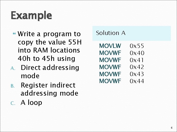
Example A. B. C. Write a program to copy the value 55 H into RAM locations 40 h to 45 h using Direct addressing mode Register indirect addressing mode A loop Solution A MOVLW MOVWF MOVWF 0 x 55 0 x 40 0 x 41 0 x 42 0 x 43 0 x 44 6
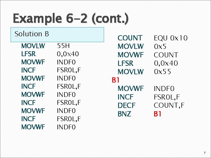
Example 6 -2 (cont. ) Solution B MOVLW LFSR MOVWF INCF MOVWF 55 H 0, 0 x 40 INDF 0 FSR 0 L, F INDF 0 COUNT MOVLW MOVWF LFSR MOVLW B 1 MOVWF INCF DECF BNZ EQU 0 x 10 0 x 5 COUNT 0, 0 x 40 0 x 55 INDF 0 FSR 0 L, F COUNT, F B 1 7
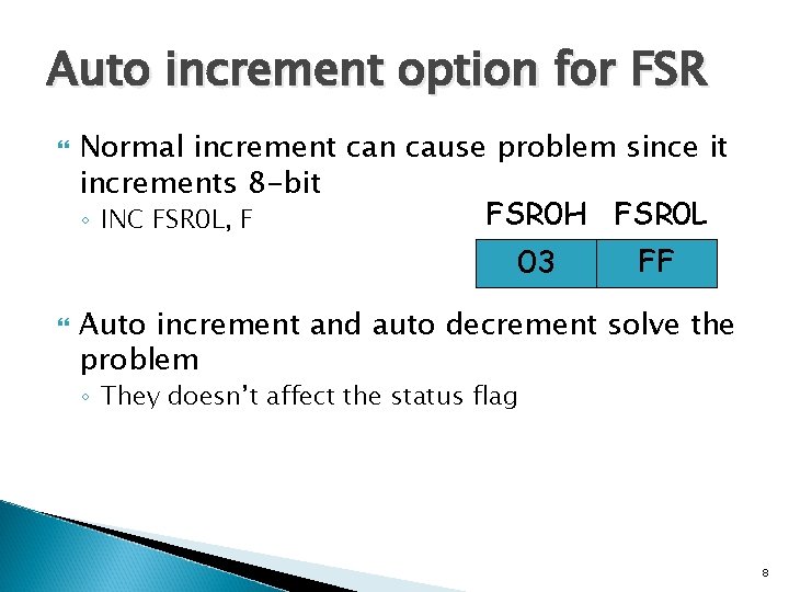
Auto increment option for FSR Normal increment can cause problem since it increments 8 -bit FSR 0 H FSR 0 L ◦ INC FSR 0 L, F 03 FF Auto increment and auto decrement solve the problem ◦ They doesn’t affect the status flag 8
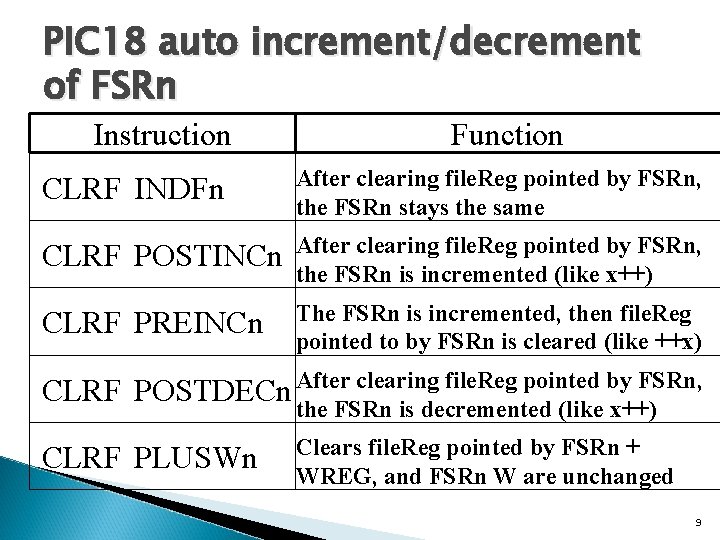
PIC 18 auto increment/decrement of FSRn Instruction Function CLRF INDFn After clearing file. Reg pointed by FSRn, the FSRn stays the same CLRF POSTINCn After clearing file. Reg pointed by FSRn, the FSRn is incremented (like x++) CLRF PREINCn The FSRn is incremented, then file. Reg pointed to by FSRn is cleared (like ++x) CLRF After clearing file. Reg pointed by FSRn, POSTDECn the FSRn is decremented (like x++) CLRF PLUSWn Clears file. Reg pointed by FSRn + WREG, and FSRn W are unchanged 9
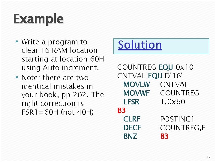
Example Write a program to clear 16 RAM location starting at location 60 H using Auto increment. Note: there are two identical mistakes in your book, pp 202. The right correction is FSR 1=60 H (not 40 H) Solution COUNTREG EQU 0 x 10 CNTVAL EQU D'16' MOVLW CNTVAL MOVWF COUNTREG LFSR 1, 0 x 60 B 3 CLRF POSTINC 1 DECF COUNTREG, F BNZ B 3 10
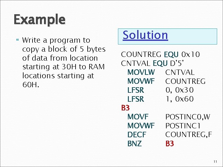
Example Write a program to copy a block of 5 bytes of data from location starting at 30 H to RAM locations starting at 60 H. Solution COUNTREG EQU 0 x 10 CNTVAL EQU D'5' MOVLW CNTVAL MOVWF COUNTREG LFSR 0, 0 x 30 LFSR 1, 0 x 60 B 3 MOVF POSTINC 0, W MOVWF POSTINC 1 DECF COUNTREG, F BNZ B 3 11
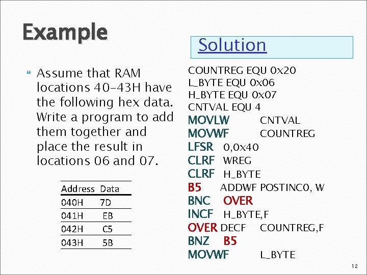
Example Assume that RAM locations 40 -43 H have the following hex data. Write a program to add them together and place the result in locations 06 and 07. Address 040 H 041 H 042 H 043 H Data 7 D EB C 5 5 B Solution COUNTREG EQU 0 x 20 L_BYTE EQU 0 x 06 H_BYTE EQU 0 x 07 CNTVAL EQU 4 MOVLW CNTVAL MOVWF COUNTREG LFSR 0, 0 x 40 CLRF WREG CLRF H_BYTE B 5 ADDWF POSTINC 0, W BNC OVER INCF H_BYTE, F OVER DECF COUNTREG, F BNZ B 5 MOVWF L_BYTE 12
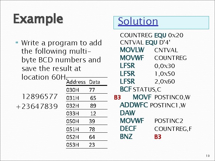
Example Solution Write a program to add the following multibyte BCD numbers and save the result at location 60 H. 12896577 +23647839 Address 030 H 031 H 032 H 033 H 050 H 051 H 052 H 053 H Data 77 65 89 12 39 78 64 23 COUNTREG EQU 0 x 20 CNTVAL EQU D'4' MOVLW CNTVAL MOVWF COUNTREG LFSR 0, 0 x 30 LFSR 1, 0 x 50 LFSR 2, 0 x 60 BCF STATUS, C B 3 MOVF POSTINC 0, W ADDWFC POSTINC 1, W DAW MOVWF DECF BNZ POSTINC 2 COUNTREG, F B 3 13
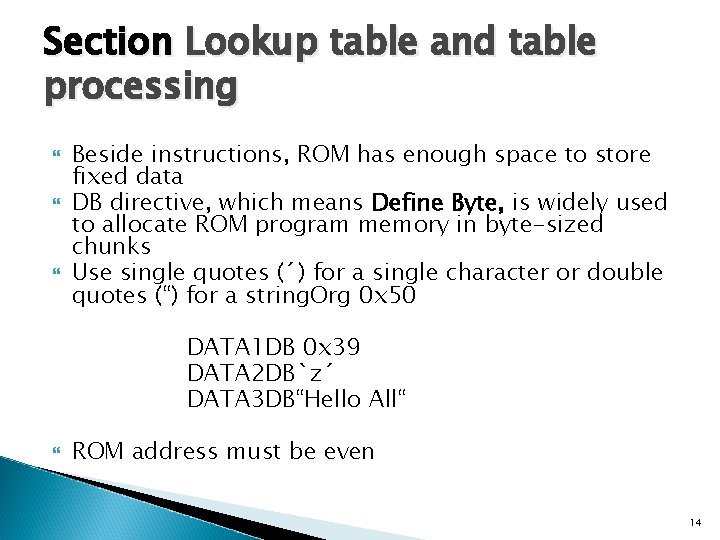
Section Lookup table and table processing Beside instructions, ROM has enough space to store fixed data DB directive, which means Define Byte, is widely used to allocate ROM program memory in byte-sized chunks Use single quotes (´) for a single character or double quotes (“) for a string. Org 0 x 50 DATA 1 DB 0 x 39 DATA 2 DB`z´ DATA 3 DB“Hello All“ ROM address must be even 14
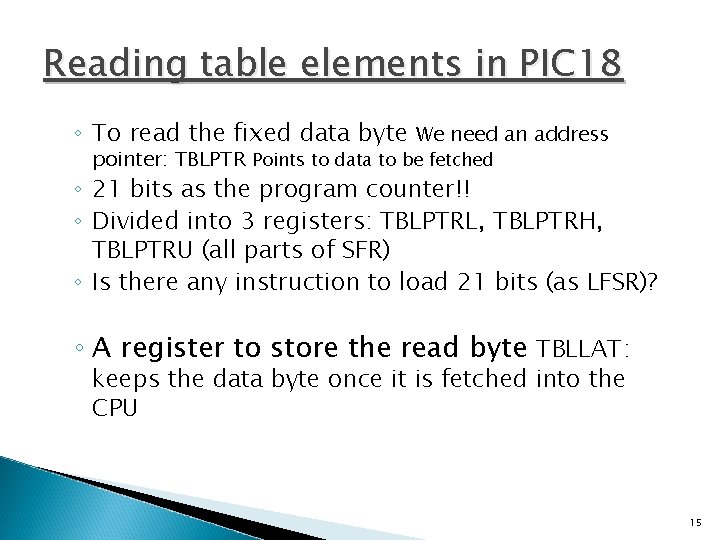
Reading table elements in PIC 18 ◦ To read the fixed data byte We need an address pointer: TBLPTR Points to data to be fetched ◦ 21 bits as the program counter!! ◦ Divided into 3 registers: TBLPTRL, TBLPTRH, TBLPTRU (all parts of SFR) ◦ Is there any instruction to load 21 bits (as LFSR)? ◦ A register to store the read byte TBLLAT: keeps the data byte once it is fetched into the CPU 15
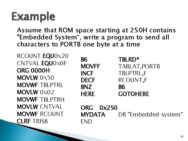
Example Assume that ROM space starting at 250 H contains "Embedded System“, write a program to send all characters to PORTB one byte at a time RCOUNT EQU 0 x 20 CNTVAL EQU 0 x 0 F ORG 0000 H MOVLW 0 x 50 MOVWF TBLPTRL MOVLW 0 x 02 MOVWF TBLPTRH MOVLW CNTVAL MOVWF RCOUNT CLRF TRISB B 6 MOVFF INCF DECF BNZ HERE TBLRD* TABLAT, PORTB TBLPTRL, F RCOUNT, F B 6 GOTOHERE ORG 0 x 250 MYDATA DB "Embedded system" END 16
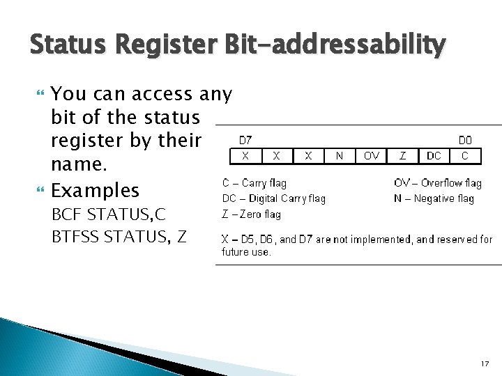
Status Register Bit-addressability You can access any bit of the status register by their name. Examples BCF STATUS, C BTFSS STATUS, Z 17
Section 6. 5: Bank switching in the PIC 18 has maximum of 4 K of RAM ◦ Not all the space used. ◦ The file. Reg is divided into 16 banks of 256 B each ◦ Every PIC 18 has the access bank (the first 128 B of RAM + SFR ) ◦ Most PIC 18 that access the data space in RAM has the ability to access any bank through setting an optional operand, called A ◦ Example: MOVWF my. Reg, A If 0 it access the default bank (default) If 1, it uses the bank selection register (BSR) to select the bank 18
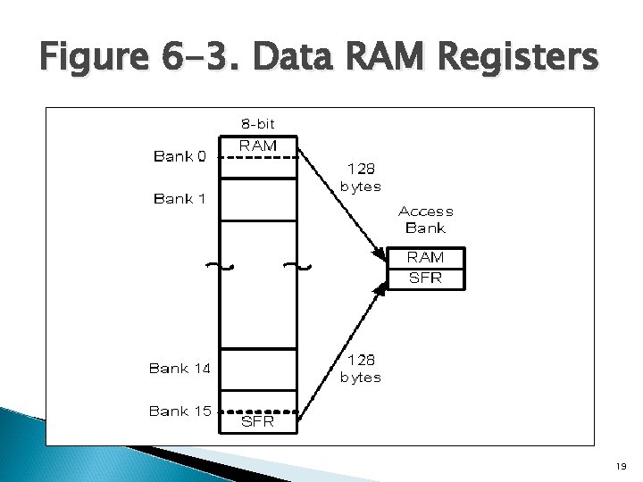
Figure 6 -3. Data RAM Registers 19
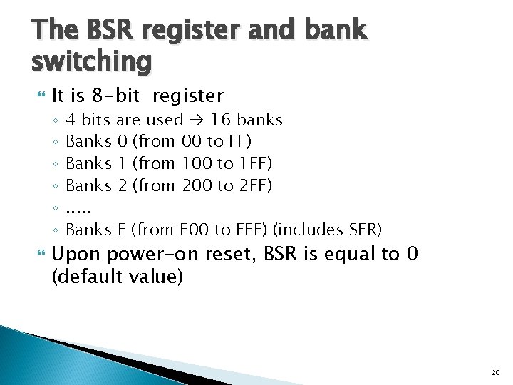
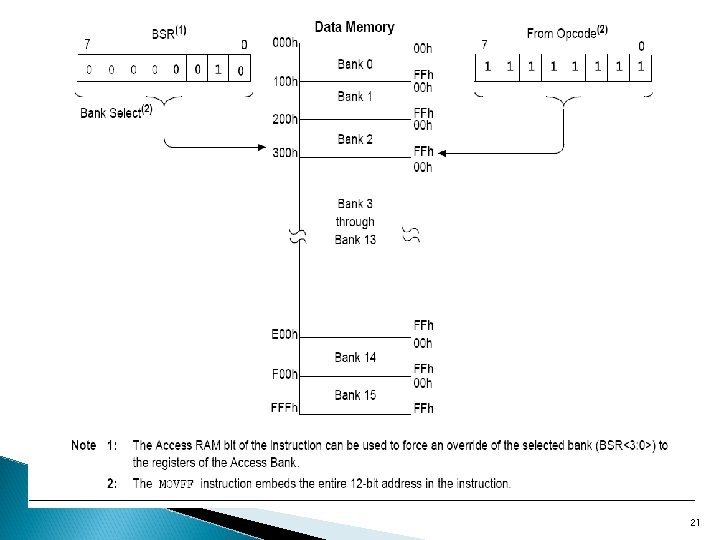
The BSR register and bank switching It is 8 -bit register ◦ ◦ ◦ 4 bits are used 16 banks Banks 0 (from 00 to FF) Banks 1 (from 100 to 1 FF) Banks 2 (from 200 to 2 FF). . . Banks F (from F 00 to FFF) (includes SFR) Upon power-on reset, BSR is equal to 0 (default value) 20
21
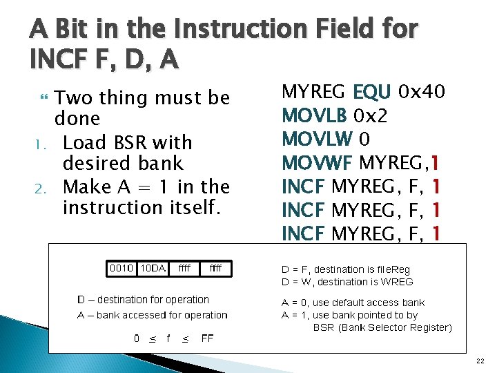
A Bit in the Instruction Field for INCF F, D, A 1. 2. Two thing must be done Load BSR with desired bank Make A = 1 in the instruction itself. MYREG EQU 0 x 40 MOVLB 0 x 2 MOVLW 0 MOVWF MYREG, 1 INCF MYREG, F, 1 22
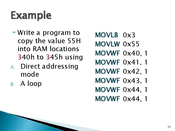
Example A. B. Write a program to copy the value 55 H into RAM locations 340 h to 345 h using Direct addressing mode A loop MOVLB MOVLW MOVWF MOVWF 0 x 3 0 x 55 0 x 40, 0 x 41, 0 x 42, 0 x 43, 0 x 44, 1 1 1 23
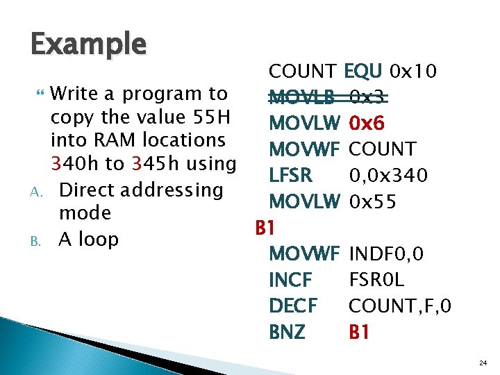
Example A. B. COUNT EQU 0 x 10 Write a program to MOVLB 0 x 3 copy the value 55 H MOVLW 0 x 6 into RAM locations MOVWF COUNT 340 h to 345 h using LFSR 0, 0 x 340 Direct addressing MOVLW 0 x 55 mode B 1 A loop MOVWF INDF 0, 0 INCF FSR 0 L DECF COUNT, F, 0 BNZ B 1 24
- Slides: 24