Chapter 5 Transistor Bias Circuits By Dr Khor

Chapter 5 Transistor Bias Circuits By: Dr. Khor Shing Fhan PPKSE

Objectives • Discuss the concept of dc biasing of a transistor for linear operation. • Analyze voltage-divider bias, base bias, emitterfeedback bias and collector-feedback bias circuits. • Basic troubleshooting for transistor bias circuits.

Outline 5. 1. 5. 2. 5. 3. 5. 4. Introduction DC operating point Voltage-divider bias Other bias methods - Emitter bias Base bias Collector-feedback bias Emitter-feedback bias 5. 5. Troubleshooting 5. 6. Summary

5. 1. Introduction • The term biasing is used for application of dc voltages to establish a fixed level of current and voltage. • A transistor must be properly biased with dc voltage to operate as a linear amplifier. • If amplifier is not biased with correct dc voltages on input and output, it can go into saturation or cutoff when the input signal applied. • There are several methods to establish DC operating point. • We will discuss some of the methods used for biasing transistors.

5. 2. DC Operating Point • The goal of amplification in most cases is to increase the amplitude of an ac signal without altering it. • Improper biasing can cause distortion in the output signal. (b) and (c). When +ve peak is limited, transistor is in cutoff. When –ve peak is limited, transistor is in saturation.

• The transistor is biased with variable voltages VCC and VBB to obtain certain values of IB, IC, IE and VCE. • The collector characteristic curves for this particular transistor are shown.

• The purpose of biasing a circuit is to establish a proper stable dc operating point (Q-point). • The dc operating point between saturation and cutoff is called the Q-point. • The goal is to set the Q-point such that it does not go into saturation or cutoff when an ac signal is applied.
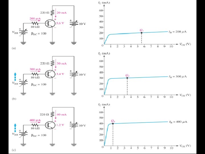

• Q-point of a circuit: is defined by the values of VCE and IC. These values are called the coordinates of Q-point. • Given βDC=100, IB = 200μA and IC=βDCIB , so IC=20 m. A and • Figure (b), VBB is increased to produce IB = 300μA and IC=30 m. A. • Figure (c), VBB is increased to produce IB = 400μA and IC=40 m. A. So, VCE is:

DC load line • Notice that when IB ↑, IC ↑ and VCE ↓ or vice-versa. • Each separate Q-point is connected through dc load line. At any point along line, values of IB, IC and VCE can be picked off the graph. • Dc load line intersect VCE-axis at 10 V, where VCE=VCC. This is cutoff point because IB and IC zero (ideally). **Actually, there is a small leakage current (ICEO), and VCE is slightly <10 V but can be neglected. • Dc load line also intersect IC-axis at 45. 5 m. A (ideally). This is saturation point because IC is max and VCE=0. **Actually, there is a small VCE(sat) across the trasistor, and IC(sat) is slightly <45. 5 m. A.

Linear operation • Region between saturation and cutoff is linear region of transistor’s operation. • The output voltage is ideally linear reproduction of input if transistor is operated in linear region. • Assume a sinusoidal ac voltage, Vin superimposed on VBB.

• Point A: corresponding to the +ve peak of the sinusoidal input voltage. • Point B: corresponds to the –ve peak of the sinusoidal input voltage. • Point Q: corresponding to the zero value of the sine wave. **VCEQ, ICQ, IBQ: dc Q-point values with no input sinusoidal voltage applied.

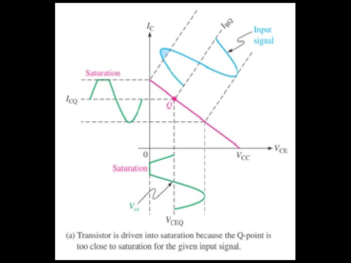
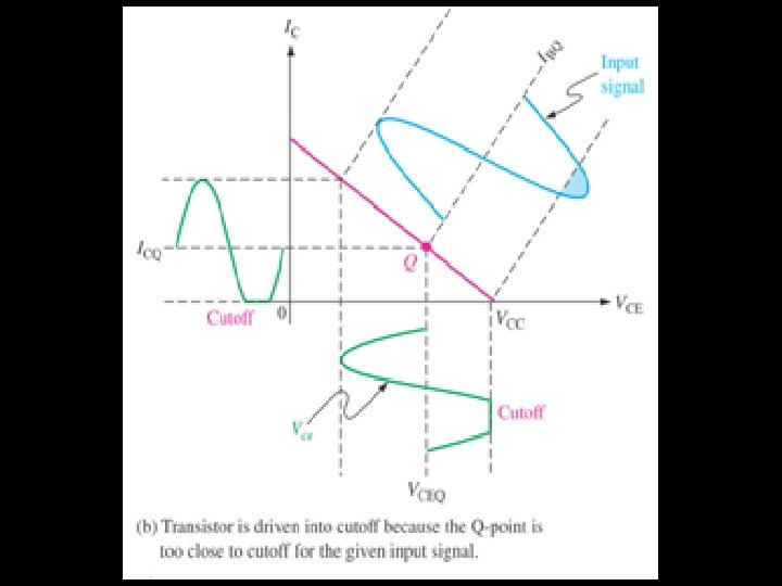
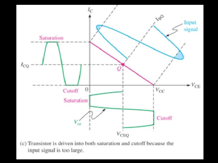
Waveform Distortion • Under certain input signal conditions (applying too much ac voltage to the base), the location of the Q-point on the load line can cause one peak of the Vce waveform to be limited or clipped. • +ve peak is limited: transistor is in cutoff. • –ve peak is limited: transistor is in saturation.

Example 5. 1 Determine Q-point in figure below and find the maximum peak value of base current for linear operation. Assume βDC=200.

Solution 5. 1 • Q-point is defined by values of IC and VCE. • Q-point is at IC=39. 6 m. A and VCE=6. 93 V. Since IC(cutoff)=0, we need to know IC(sat) to determine variation in IC can occur and still in linear operation. • Before saturation is reached, IC can increase an amount equal to: IC(sat) – ICQ = 60. 6 m. A – 39. 6 m. A = 21 m. A.
")
• However, IC can decrease by 39. 6 m. A before cutoff (IC=0) is reached. The Q-point is closer to saturation point than to cutoff point. The 21 m. A is the max peak variation of IC. • The max peak variation of IB is: IC(sat)= 21 m. A ICQ= 39. 6 m. A VCEQ

5. 3. VOLTAGE-DIVIDER BIAS VB • Voltage-divider bias is the most widely used type of bias circuit. • Only one power supply is needed and voltage-divider bias is more stable ( independent) than other bias types. • Dc bias voltage at base of transistor is developed by a resistive voltagedivider consists of R 1 and R 2. • VCC is dc collector supply voltage. Two current paths between point A and ground: (a). through R 2 and (b). through BE-junction and RE.

DC Input resistance at transistor base • VIN is applied between base and ground, IIN is the input current into base. • Resistance from base to ground (RIN(base): • RIN(base) = VB / IB Since IC =βDCIB =IE,
: IB << than I 2: Bias circuit is viewed as voltage")
• (Stiff): IB << than I 2: Bias circuit is viewed as voltage divider of R 1 and R 2 as shown in Figure (a). VB VB VB • (Not Stiff): IB is not small enough to be neglected: Dc input resistance, RIN(base) must be considered and should be combined in parallel with R 2 as shown in figure (b).
 >>10 R 2: Stiff • If RIN(base) < 10 R")
• If RIN(base) >>10 R 2: Stiff • If RIN(base) < 10 R 2: Not Stiff

Analyze Stiff voltage-divider circuit for IB << I 2: Ø emitter voltage, VE = VB – VBE Ø Using Ohm’s Law: emitter current, IE = VE / RE Ø And, IC ≈ IE VC = VCC – ICRC • Once know VC and VE, VCE can be determine: VCE = VC – VE

Example 5. 2 • Determine VCE and IC in voltage-divider biased transistor circuit below if βDC=100.

Solution 5. 2 The base voltage is So, emitter voltage: And emitter current: Therefore: And

Example 5. 3 Determine the dc input resistance of the transistor in Figure below. Given RE=1. 0 kΩ, βDC=125 and VB=4 V.

Thevenin’s Theorem applied to Voltage-divider Bias • Using Thevenin’s theorem to get an equivalent baseemitter circuit in Figure (a), and can be redrawn as in Figure (b). • Apply Thevenin’s Theorem to the circuit left of point A.

• The voltage at point A with respect to ground: • Resistance is: • Apply KVL on base-emitter loop:

Voltage-Divider Bias for PNP Transistor • Pnp transistor has opposite polarities from npn. • To obtain pnp, required (a). negative collector supply voltage or (b). with a positive emitter supply voltage. • The analysis of pnp is basically the same as npn.

Negative Collector Supply Voltage • Apply KVL around Base-emitter circuit: • By Thevenin’s Theorem: • Base Current is: • Emitter current:

Positive Emitter Supply Voltage • Apply KVL around Base-emitter circuit: • By Thevenin’s Theorem: • Base Current is: • Emitter current:

Example 5. 4 Find IC and VCE for the pnp transistor circuit in Figure below.

Apply Thevenin’s Theorem: Determine IE: **if the –ve sign on IE indicates that the assumed current direction in the KIrchhoff’s analysis is opposite from the actual current direction.

From IE, determine IC and VCE as follow:

Example 5. 5 Find IC and VCE for a pnp transistor circuit. Solution: Apply Thevenin’s Theorem: Determine IE:

From IE, determine IC and VCE as follow:
 = 0. 7 V. RE =")
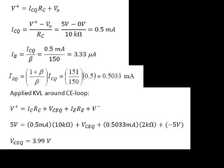
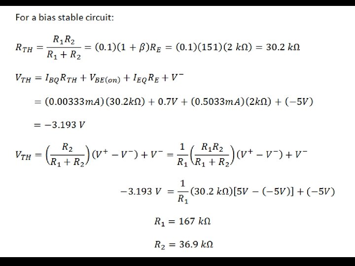
The circuit is given β = 150, VBE(on) = 0. 7 V. RE = 2 kΩ, RC = 10 kΩ. Design a bias stable circuit that output voltage is zero. Calculate ICQ, VCEQ, R 1 and R 2.
. Emitter Bias (2). Base Bias (3). Emitter-Feedback Bias")
5. 4. Other Bias Methods (1). Emitter Bias (2). Base Bias (3). Emitter-Feedback Bias (4). Collector-Feedback Bias
. Emitter Bias • Uses both a +ve and a -ve supply voltage. •")
(1). Emitter Bias • Uses both a +ve and a -ve supply voltage. • Provides excellent bias stability in spite of changes in β or temperature. • VEE supply voltage forward-biases the BEjunction.

• Apply KVL and Ohm’s Law: • Since IC≈IE and IC= DCIB, so: • Solve for IE or IC: • Emitter voltage: VE = VEE + IERE • Base voltage: VB = VE + VBE • Collector voltage: VC = VCC – ICRC
 for the circuit below")
Example 5. 6 Determine how much the Q-point (IC, VCE) for the circuit below will change if βDC increase from 100 to 200 when one transistor is replaced by another.

For βDC=100, Therefore, For βDC=200, Therefore,

The percent change in IC as βDC changes from 100 to 200 is: The percent change in VCE is:
. Base Bias • Is common in switching circuits. **KVL apply on base circuit.")
(2). Base Bias • Is common in switching circuits. **KVL apply on base circuit. VCC – VRB – VBE = 0 , VRB=IBRB VCC – IBRB – VBE =0 • So, IB: **KVL apply on around collector circuit. VCC – ICRC – VCE = 0, so • We know that IC = βDCIB,

Q-Point Stability of Base Bias • the equation of IC is dependent on DC. When DC vary, VCE also vary, thus changing Q-point of transistor. • This type of circuit is extremely DC-dependent and very unstable. • Recall that DC changes with temperature and IC.
 for the circuit below")
Example 5. 7 Determine how much the Q-point (IC, VCE) for the circuit below will change over a temperature range where βDC increase from 100 to 200.

For βDC=100, For βDC=200, The percent change in IC as βDC changes from 100 to 200 is:

The percent change in VCE is: ** Q-point is very dependent on βDC in this circuit and therefore make the base bias arrangement very unreliable.
. Emitter-Feedback Bias • A emitter resistor is added to the basebias circuit. •")
(3). Emitter-Feedback Bias • A emitter resistor is added to the basebias circuit. • This bias is to help make base bias more predictable with –ve feedback. • If IC try to ↑, VE ↑, VB ↑ because VB=VE+VBE. Then, ↓ the VRB, thus ↓ IB and keeping the IC from increasing. **KVL on base circuit: Still dependent on βDC.
 for the circuit below")
Example 5. 8 Determine how much the Q-point (IC, VCE) for the circuit below will change where βDC increase from 100 to 200.

For βDC=100, For βDC=200, The percent change:
. Collector-Feedback Bias • Base resistor RB is connected to the collector rather than")
(4). Collector-Feedback Bias • Base resistor RB is connected to the collector rather than to VCC. • The VC provides the bias for the BE -junction. • The negative feedback creates an “offsetting” effect that tends to keep the Q-point stable. • IC ↑, VRC ↑, VC ↓, VRB ↓, IC ↓; In turn, VRC ↓, VC ↑.

Analysis of collector-feedback circuit • By Ohm’s Law, the base current: • Assume IC>>IB. Collector voltage: • And, • So, collector current: • Since emitter is ground, VCE = VC.
 for the circuit below. Solution: The")
Example 5. 9 Calculate the Q-point (IC, VCE) for the circuit below. Solution: The collector current is: The collector-to-emitter voltage is:

Q-Point Stability Over Temperature • Temperature ↑, βDC ↑, VBE ↓. • As βDC ↑, IC ↑. • As VBE ↓, IB ↑, IC ↑, so VRC ↑, VC ↓, VRB ↓. • Thus reducing IB, offsetting the attempted increase in IC and the attempted decrease in V C. • So, the collector-feedback circuit maintains a relatively stable Q-point.

TROUBLESHOOTING • Figure below show a typical voltage divider circuit with correct voltage readings. Knowing these voltages is a requirement before logical troubleshooting can be applied. We will discuss some of the faults and symptoms.

All indicated faults

Fault 1: R 1 Open • With no bias the transistor is in cutoff. • VB =0 V and IB=0 A. • Transistor is nonconducting, IC=0 A and VRC=0 V. • Thus VC = VCC (10 V) • Since IB and IC=0 A, IE=0 A as well and VE=0 V. Fault 2: Resistor RE Open • Transistor is in cutoff. • Since IC=0, VRC=0 and VC=VCC (10 V).
, IC=0 A and VC=VCC=10")
Fault 3: Base internally open • Transistor is nonconducting (cutoff), IC=0 A and VC=VCC=10 V. • Just as the case of open RE, VB=3. 2 V. • VC=VCC (10 V). • VE=0 V because no IE through RE. Fault 4: BE-junction open • Transistor is nonconducting (cutoff), IC=0 A and VC=VCC=10 V. • Just as the case of open RE, VB=3. 2 V. • VC=VCC (10 V). • VE=0 V since no IE through RE.
, IC=0 A and VC=VCC=10 V.")
Fault 5: BC-junction open • Transistor is nonconducting (cutoff), IC=0 A and VC=VCC=10 V. • VB=1. 11 V because of more IB flow through emitter. • VC=VCC (10 V). • VE=0. 41 V because of small current flow from forwardbiased BE-junction.
, IC=0 A. • The circuit")
Fault 6: RC open • Transistor is nonconducting (cutoff), IC=0 A. • The circuit is same as Fault 5. therefore VB=1. 11 V and since BE-junction is forward bias: • When a voltmeter is connected to collector to measure VC, a current path is provided through the internal impedance of the meter and the BC-junction (forward bias):

Fault 7: R 2 open • When R 2 open, VB and IB increase from their normal value because the voltage divider now is formed by R 1 and RIN(base). • So: • VE=3. 13 V because of increased current. • VC=3. 33 V because of increased conduction of transistor.
.")
SUMMARY • The purpose of biasing is to establish a stable operating point (Q-point). • The Q-point is the best point for operation of a transistor for a given collector current. • The dc load line helps to establish the Q-point for a given collector current. • The linear region of a transistor is the region of operation within saturation and cutoff.

• Voltage-divider bias is most widely used because it is stable and uses only one voltage supply. • Base bias is very unstable because it is dependent. • Emitter bias is stable but require two voltage supplies. • Collector-feedback bias is relatively stable when compared to base bias, but not as stable as voltage-divider bias.

End

Q-Point Stability of Emitter Bias • shows that the circuit is dependent on DC and VBE. • If RE>>RB/ DC: (IE essentially independent of DC) • If VEE>>VBE: (IE essentially independent of VBE) • If IE is independent of DC and VBE, the emitter bias can provide a stable Q-point if properly designed.

Solution 5. 2 1. Determine dc input resistance at base to see if it can be neglected. 2. RIN(base)=10 R 2, so neglect RIN(base). Then, find base voltage: 3. So, emitter voltage: 4. And emitter current: 5. Thus, 6. And VCE is

Analysis of voltage bias for pnp transistor • Base voltage: • Emitter voltage: • By Ohm’s Law, • And,
- Slides: 71