Chapter 5 ThreadLevel Parallelism 2019 Elsevier Inc All

- Slides: 41

Chapter 5 Thread-Level Parallelism © 2019 Elsevier Inc. All rights reserved.

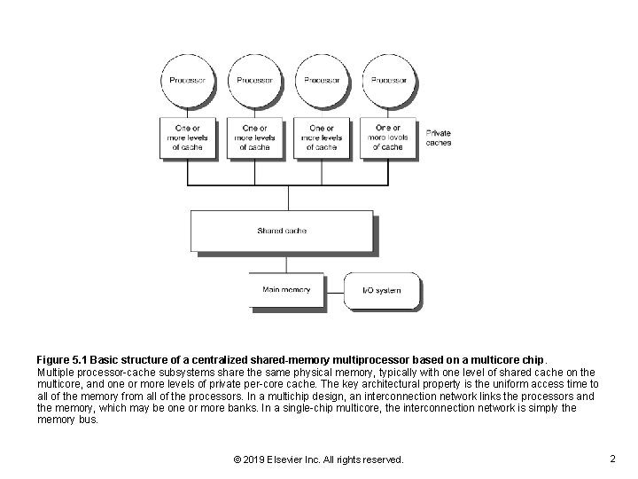
Figure 5. 1 Basic structure of a centralized shared-memory multiprocessor based on a multicore chip. Multiple processor-cache subsystems share the same physical memory, typically with one level of shared cache on the multicore, and one or more levels of private per-core cache. The key architectural property is the uniform access time to all of the memory from all of the processors. In a multichip design, an interconnection network links the processors and the memory, which may be one or more banks. In a single-chip multicore, the interconnection network is simply the memory bus. © 2019 Elsevier Inc. All rights reserved. 2

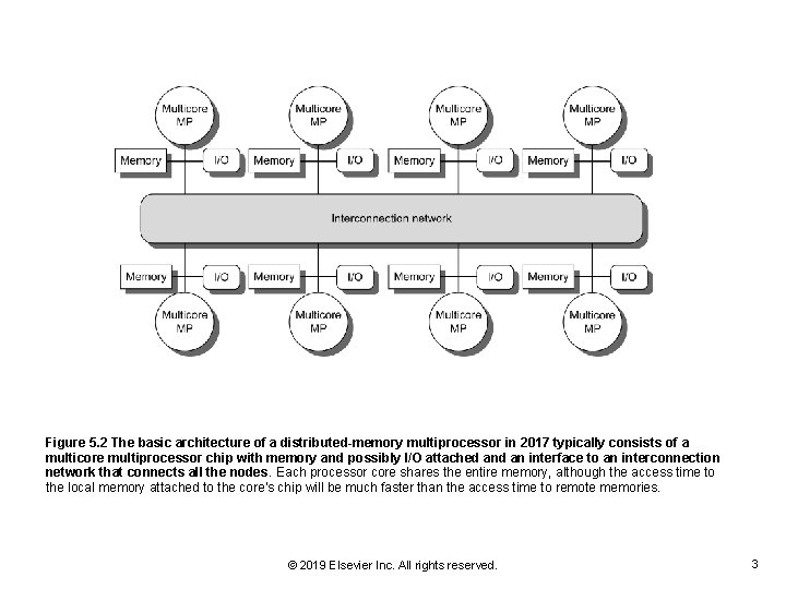
Figure 5. 2 The basic architecture of a distributed-memory multiprocessor in 2017 typically consists of a multicore multiprocessor chip with memory and possibly I/O attached an interface to an interconnection network that connects all the nodes. Each processor core shares the entire memory, although the access time to the local memory attached to the core's chip will be much faster than the access time to remote memories. © 2019 Elsevier Inc. All rights reserved. 3

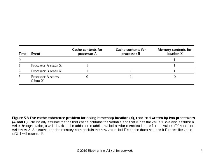
Figure 5. 3 The cache coherence problem for a single memory location (X), read and written by two processors (A and B). We initially assume that neither cache contains the variable and that X has the value 1. We also assume a write-through cache; a write-back cache adds some additional but similar complications. After the value of X has been written by A, A's cache and the memory both contain the new value, but B's cache does not, and if B reads the value of X it will receive 1!. © 2019 Elsevier Inc. All rights reserved. 4

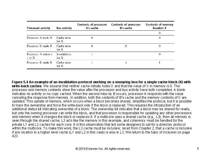
Figure 5. 4 An example of an invalidation protocol working on a snooping bus for a single cache block (X) with write-back caches. We assume that neither cache initially holds X and that the value of X in memory is 0. The processor and memory contents show the value after the processor and bus activity have both completed. A blank indicates no activity or no copy cached. When the second miss by B occurs, processor A responds with the value canceling the response from memory. In addition, both the contents of B's cache and the memory contents of X are updated. This update of memory, which occurs when a block becomes shared, simplifies the protocol, but it is possible to track the ownership and force the write-back only if the block is replaced. This requires the introduction of an additional status bit indicating ownership of a block. The ownership bit indicates that a block may be shared for reads, but only the owning processor can write the block, and that processor is responsible for updating any other processors and memory when it changes the block or replaces it. If a multicore uses a shared cache (e. g. , L 3), then all memory is seen through the shared cache; L 3 acts like the memory in this example, and coherency must be handled for the private L 1 and L 2 caches for each core. It is this observation that led some designers to opt for a directory protocol within the multicore. To make this work, the L 3 cache must be inclusive; recall from Chapter 2, that a cache is inclusive if any location in a higher level cache (L 1 and L 2 in this case) is also in L 3. We return to the topic of inclusion on page 423. © 2019 Elsevier Inc. All rights reserved. 5

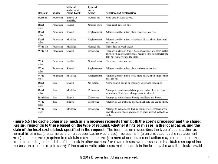
Figure 5. 5 The cache coherence mechanism receives requests from both the core's processor and the shared bus and responds to these based on the type of request, whether it hits or misses in the local cache, and the state of the local cache block specified in the request. The fourth column describes the type of cache action as normal hit or miss (the same as a uniprocessor cache would see), replacement (a uniprocessor cache replacement miss), or coherence (required to maintain cache coherence); a normal or replacement action may cause a coherence action depending on the state of the block in other caches. For read, misses, write misses, or invalidates snooped from the bus, an action is required only if the read or write addresses match a block in the local cache and the block is valid. © 2019 Elsevier Inc. All rights reserved. 6

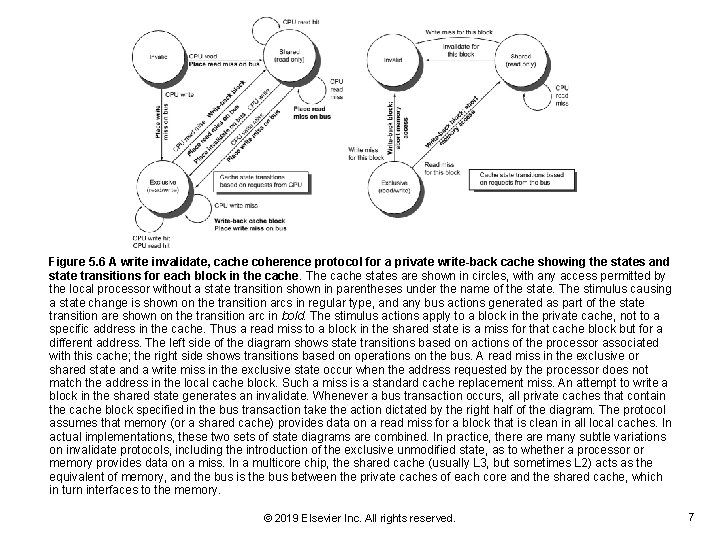
Figure 5. 6 A write invalidate, cache coherence protocol for a private write-back cache showing the states and state transitions for each block in the cache. The cache states are shown in circles, with any access permitted by the local processor without a state transition shown in parentheses under the name of the state. The stimulus causing a state change is shown on the transition arcs in regular type, and any bus actions generated as part of the state transition are shown on the transition arc in bold. The stimulus actions apply to a block in the private cache, not to a specific address in the cache. Thus a read miss to a block in the shared state is a miss for that cache block but for a different address. The left side of the diagram shows state transitions based on actions of the processor associated with this cache; the right side shows transitions based on operations on the bus. A read miss in the exclusive or shared state and a write miss in the exclusive state occur when the address requested by the processor does not match the address in the local cache block. Such a miss is a standard cache replacement miss. An attempt to write a block in the shared state generates an invalidate. Whenever a bus transaction occurs, all private caches that contain the cache block specified in the bus transaction take the action dictated by the right half of the diagram. The protocol assumes that memory (or a shared cache) provides data on a read miss for a block that is clean in all local caches. In actual implementations, these two sets of state diagrams are combined. In practice, there are many subtle variations on invalidate protocols, including the introduction of the exclusive unmodified state, as to whether a processor or memory provides data on a miss. In a multicore chip, the shared cache (usually L 3, but sometimes L 2) acts as the equivalent of memory, and the bus is the bus between the private caches of each core and the shared cache, which in turn interfaces to the memory. © 2019 Elsevier Inc. All rights reserved. 7

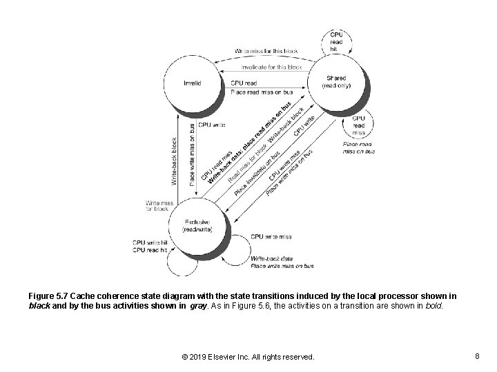
Figure 5. 7 Cache coherence state diagram with the state transitions induced by the local processor shown in black and by the bus activities shown in gray. As in Figure 5. 6, the activities on a transition are shown in bold. © 2019 Elsevier Inc. All rights reserved. 8

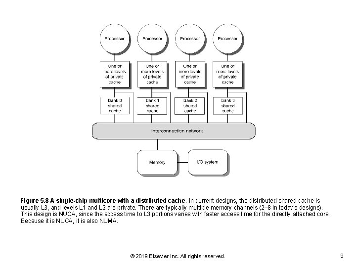
Figure 5. 8 A single-chip multicore with a distributed cache. In current designs, the distributed shared cache is usually L 3, and levels L 1 and L 2 are private. There are typically multiple memory channels (2– 8 in today's designs). This design is NUCA, since the access time to L 3 portions varies with faster access time for the directly attached core. Because it is NUCA, it is also NUMA. © 2019 Elsevier Inc. All rights reserved. 9

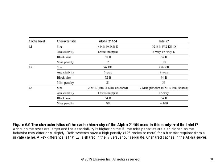
Figure 5. 9 The characteristics of the cache hierarchy of the Alpha 21164 used in this study and the Intel i 7. Although the sizes are larger and the associativity is higher on the i 7, the miss penalties are also higher, so the behavior may differ only slightly. Both systems have a high penalty (125 cycles or more) for a transfer required from a private cache. A key difference is that L 3 is shared in the i 7 versus four separate, unshared caches in the Alpha server. © 2019 Elsevier Inc. All rights reserved. 10

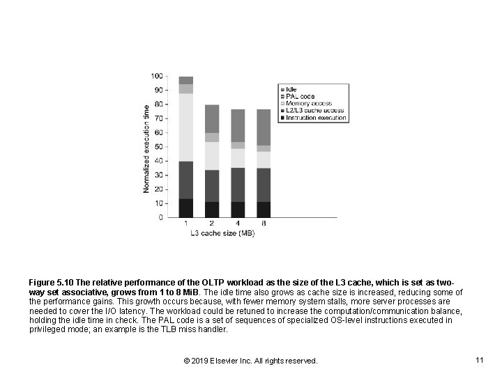
Figure 5. 10 The relative performance of the OLTP workload as the size of the L 3 cache, which is set as twoway set associative, grows from 1 to 8 Mi. B. The idle time also grows as cache size is increased, reducing some of the performance gains. This growth occurs because, with fewer memory system stalls, more server processes are needed to cover the I/O latency. The workload could be retuned to increase the computation/communication balance, holding the idle time in check. The PAL code is a set of sequences of specialized OS-level instructions executed in privileged mode; an example is the TLB miss handler. © 2019 Elsevier Inc. All rights reserved. 11

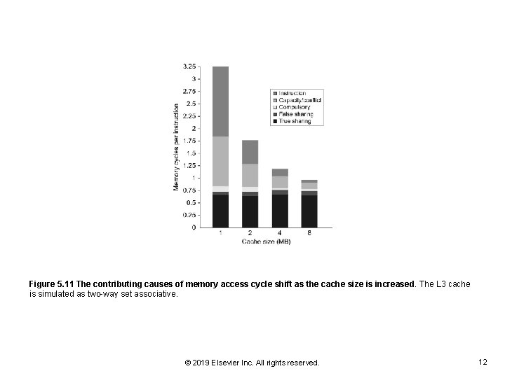
Figure 5. 11 The contributing causes of memory access cycle shift as the cache size is increased. The L 3 cache is simulated as two-way set associative. © 2019 Elsevier Inc. All rights reserved. 12

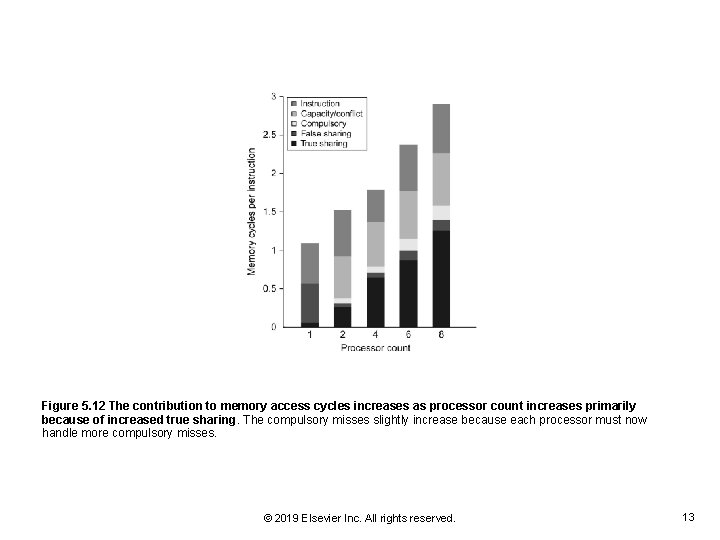
Figure 5. 12 The contribution to memory access cycles increases as processor count increases primarily because of increased true sharing. The compulsory misses slightly increase because each processor must now handle more compulsory misses. © 2019 Elsevier Inc. All rights reserved. 13

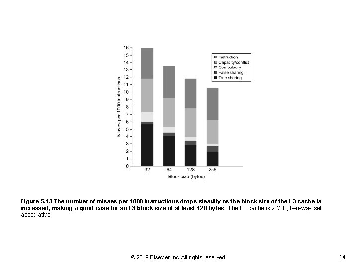
Figure 5. 13 The number of misses per 1000 instructions drops steadily as the block size of the L 3 cache is increased, making a good case for an L 3 block size of at least 128 bytes. The L 3 cache is 2 Mi. B, two-way set associative. © 2019 Elsevier Inc. All rights reserved. 14

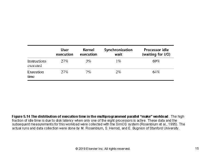
Figure 5. 14 The distribution of execution time in the multiprogrammed parallel “make” workload. The high fraction of idle time is due to disk latency when only one of the eight processors is active. These data and the subsequent measurements for this workload were collected with the Sim. OS system (Rosenblum et al. , 1995). The actual runs and data collection were done by M. Rosenblum, S. Herrod, and E. Bugnion of Stanford University. © 2019 Elsevier Inc. All rights reserved. 15

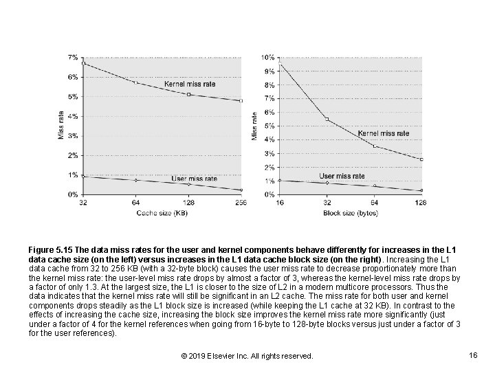
Figure 5. 15 The data miss rates for the user and kernel components behave differently for increases in the L 1 data cache size (on the left) versus increases in the L 1 data cache block size (on the right). Increasing the L 1 data cache from 32 to 256 KB (with a 32 -byte block) causes the user miss rate to decrease proportionately more than the kernel miss rate: the user-level miss rate drops by almost a factor of 3, whereas the kernel-level miss rate drops by a factor of only 1. 3. At the largest size, the L 1 is closer to the size of L 2 in a modern multicore processors. Thus the data indicates that the kernel miss rate will still be significant in an L 2 cache. The miss rate for both user and kernel components drops steadily as the L 1 block size is increased (while keeping the L 1 cache at 32 KB). In contrast to the effects of increasing the cache size, increasing the block size improves the kernel miss rate more significantly (just under a factor of 4 for the kernel references when going from 16 -byte to 128 -byte blocks versus just under a factor of 3 for the user references). © 2019 Elsevier Inc. All rights reserved. 16

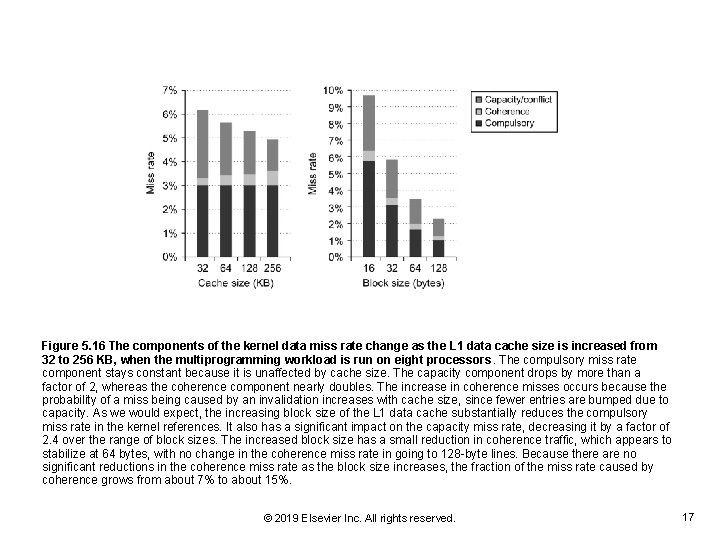
Figure 5. 16 The components of the kernel data miss rate change as the L 1 data cache size is increased from 32 to 256 KB, when the multiprogramming workload is run on eight processors. The compulsory miss rate component stays constant because it is unaffected by cache size. The capacity component drops by more than a factor of 2, whereas the coherence component nearly doubles. The increase in coherence misses occurs because the probability of a miss being caused by an invalidation increases with cache size, since fewer entries are bumped due to capacity. As we would expect, the increasing block size of the L 1 data cache substantially reduces the compulsory miss rate in the kernel references. It also has a significant impact on the capacity miss rate, decreasing it by a factor of 2. 4 over the range of block sizes. The increased block size has a small reduction in coherence traffic, which appears to stabilize at 64 bytes, with no change in the coherence miss rate in going to 128 -byte lines. Because there are no significant reductions in the coherence miss rate as the block size increases, the fraction of the miss rate caused by coherence grows from about 7% to about 15%. © 2019 Elsevier Inc. All rights reserved. 17

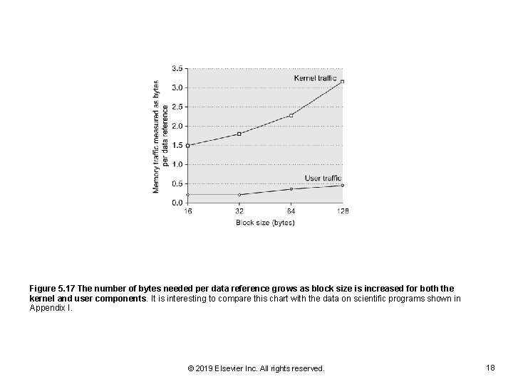
Figure 5. 17 The number of bytes needed per data reference grows as block size is increased for both the kernel and user components. It is interesting to compare this chart with the data on scientific programs shown in Appendix I. © 2019 Elsevier Inc. All rights reserved. 18

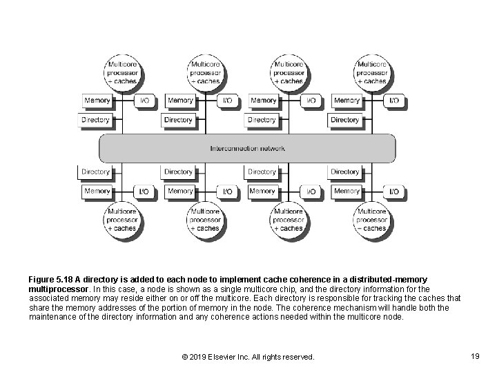
Figure 5. 18 A directory is added to each node to implement cache coherence in a distributed-memory multiprocessor. In this case, a node is shown as a single multicore chip, and the directory information for the associated memory may reside either on or off the multicore. Each directory is responsible for tracking the caches that share the memory addresses of the portion of memory in the node. The coherence mechanism will handle both the maintenance of the directory information and any coherence actions needed within the multicore node. © 2019 Elsevier Inc. All rights reserved. 19

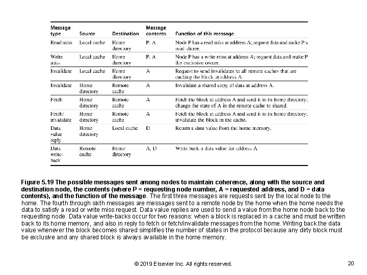
Figure 5. 19 The possible messages sent among nodes to maintain coherence, along with the source and destination node, the contents (where P = requesting node number, A = requested address, and D = data contents), and the function of the message. The first three messages are requests sent by the local node to the home. The fourth through sixth messages are messages sent to a remote node by the home when the home needs the data to satisfy a read or write miss request. Data value replies are used to send a value from the home node back to the requesting node. Data value write-backs occur for two reasons: when a block is replaced in a cache and must be written back to its home memory, and also in reply to fetch or fetch/invalidate messages from the home. Writing back the data value whenever the block becomes shared simplifies the number of states in the protocol because any dirty block must be exclusive and any shared block is always available in the home memory. © 2019 Elsevier Inc. All rights reserved. 20

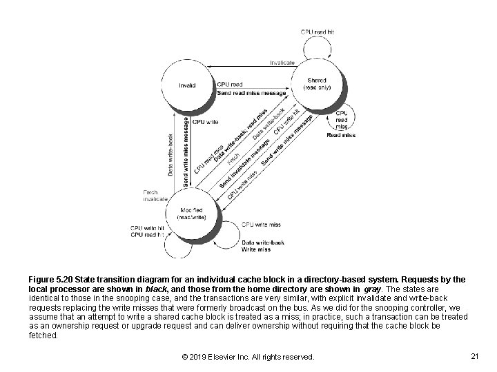
Figure 5. 20 State transition diagram for an individual cache block in a directory-based system. Requests by the local processor are shown in black, and those from the home directory are shown in gray. The states are identical to those in the snooping case, and the transactions are very similar, with explicit invalidate and write-back requests replacing the write misses that were formerly broadcast on the bus. As we did for the snooping controller, we assume that an attempt to write a shared cache block is treated as a miss; in practice, such a transaction can be treated as an ownership request or upgrade request and can deliver ownership without requiring that the cache block be fetched. © 2019 Elsevier Inc. All rights reserved. 21

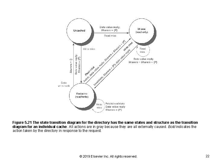
Figure 5. 21 The state transition diagram for the directory has the same states and structure as the transition diagram for an individual cache. All actions are in gray because they are all externally caused. Bold indicates the action taken by the directory in response to the request. © 2019 Elsevier Inc. All rights reserved. 22

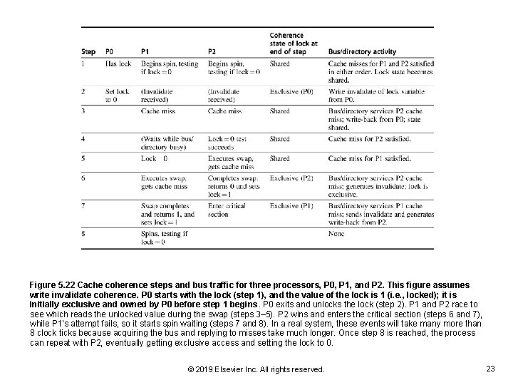
Figure 5. 22 Cache coherence steps and bus traffic for three processors, P 0, P 1, and P 2. This figure assumes write invalidate coherence. P 0 starts with the lock (step 1), and the value of the lock is 1 (i. e. , locked); it is initially exclusive and owned by P 0 before step 1 begins. P 0 exits and unlocks the lock (step 2). P 1 and P 2 race to see which reads the unlocked value during the swap (steps 3– 5). P 2 wins and enters the critical section (steps 6 and 7), while P 1's attempt fails, so it starts spin waiting (steps 7 and 8). In a real system, these events will take many more than 8 clock ticks because acquiring the bus and replying to misses take much longer. Once step 8 is reached, the process can repeat with P 2, eventually getting exclusive access and setting the lock to 0. © 2019 Elsevier Inc. All rights reserved. 23

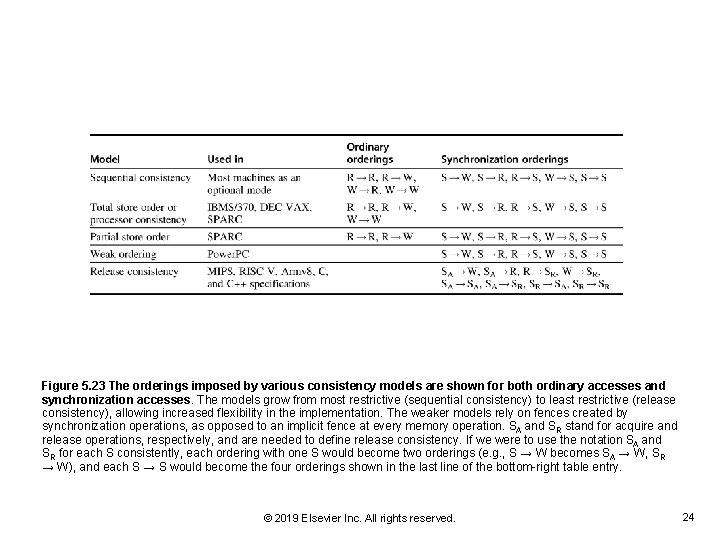
Figure 5. 23 The orderings imposed by various consistency models are shown for both ordinary accesses and synchronization accesses. The models grow from most restrictive (sequential consistency) to least restrictive (release consistency), allowing increased flexibility in the implementation. The weaker models rely on fences created by synchronization operations, as opposed to an implicit fence at every memory operation. SA and SR stand for acquire and release operations, respectively, and are needed to define release consistency. If we were to use the notation SA and SR for each S consistently, each ordering with one S would become two orderings (e. g. , S → W becomes SA → W, SR → W), and each S → S would become the four orderings shown in the last line of the bottom-right table entry. © 2019 Elsevier Inc. All rights reserved. 24

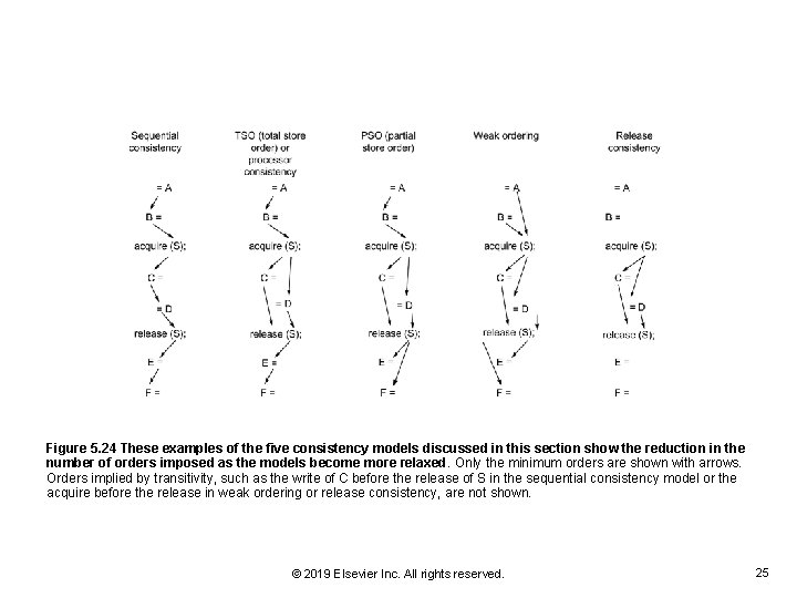
Figure 5. 24 These examples of the five consistency models discussed in this section show the reduction in the number of orders imposed as the models become more relaxed. Only the minimum orders are shown with arrows. Orders implied by transitivity, such as the write of C before the release of S in the sequential consistency model or the acquire before the release in weak ordering or release consistency, are not shown. © 2019 Elsevier Inc. All rights reserved. 25

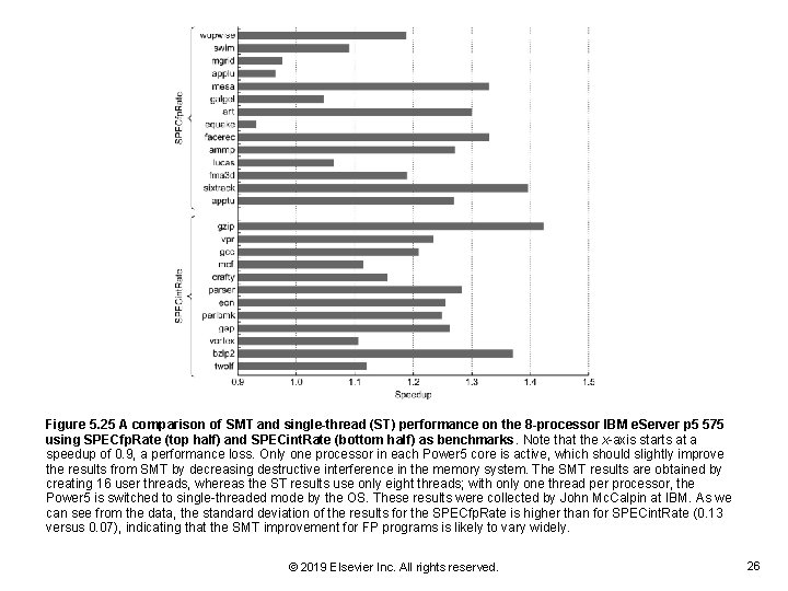
Figure 5. 25 A comparison of SMT and single-thread (ST) performance on the 8 -processor IBM e. Server p 5 575 using SPECfp. Rate (top half) and SPECint. Rate (bottom half) as benchmarks. Note that the x-axis starts at a speedup of 0. 9, a performance loss. Only one processor in each Power 5 core is active, which should slightly improve the results from SMT by decreasing destructive interference in the memory system. The SMT results are obtained by creating 16 user threads, whereas the ST results use only eight threads; with only one thread per processor, the Power 5 is switched to single-threaded mode by the OS. These results were collected by John Mc. Calpin at IBM. As we can see from the data, the standard deviation of the results for the SPECfp. Rate is higher than for SPECint. Rate (0. 13 versus 0. 07), indicating that the SMT improvement for FP programs is likely to vary widely. © 2019 Elsevier Inc. All rights reserved. 26

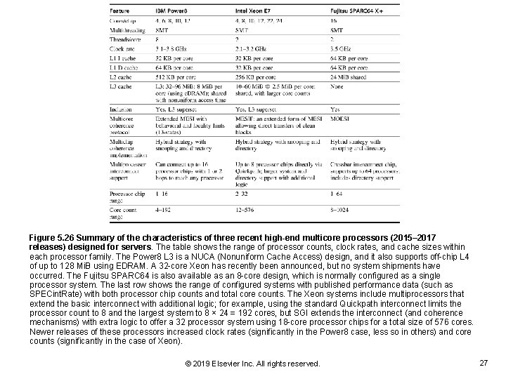
Figure 5. 26 Summary of the characteristics of three recent high-end multicore processors (2015– 2017 releases) designed for servers. The table shows the range of processor counts, clock rates, and cache sizes within each processor family. The Power 8 L 3 is a NUCA (Nonuniform Cache Access) design, and it also supports off-chip L 4 of up to 128 Mi. B using EDRAM. A 32 -core Xeon has recently been announced, but no system shipments have occurred. The Fujitsu SPARC 64 is also available as an 8 -core design, which is normally configured as a single processor system. The last row shows the range of configured systems with published performance data (such as SPECint. Rate) with both processor chip counts and total core counts. The Xeon systems include multiprocessors that extend the basic interconnect with additional logic; for example, using the standard Quickpath interconnect limits the processor count to 8 and the largest system to 8 × 24 = 192 cores, but SGI extends the interconnect (and coherence mechanisms) with extra logic to offer a 32 processor system using 18 -core processor chips for a total size of 576 cores. Newer releases of these processors increased clock rates (significantly in the Power 8 case, less so in others) and core counts (significantly in the case of Xeon). © 2019 Elsevier Inc. All rights reserved. 27

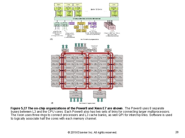
Figure 5. 27 The on-chip organizations of the Power 8 and Xeon E 7 are shown. The Power 8 uses 8 separate buses between L 3 and the CPU cores. Each Power 8 also has two sets of links for connecting larger multiprocessors. The Xeon uses three rings to connect processors and L 3 cache banks, as well QPI for interchip links. Software is used to logically associate half the cores with each memory channel. © 2019 Elsevier Inc. All rights reserved. 28

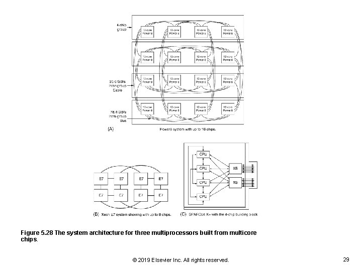
Figure 5. 28 The system architecture for three multiprocessors built from multicore chips. © 2019 Elsevier Inc. All rights reserved. 29

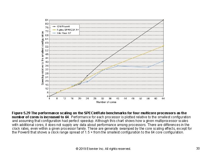
Figure 5. 29 The performance scaling on the SPECint. Rate benchmarks for four multicore processors as the number of cores is increased to 64. Performance for each processor is plotted relative to the smallest configuration and assuming that configuration had perfect speedup. Although this chart shows how a given multiprocessor scales with additional cores, it does not supply any data about performance among processors. There are differences in the clock rates, even within a given processor family. These are generally swamped by the core scaling effects, except for the Power 8 that shows a clock range spread of 1. 5 × from the smallest configuration to the 64 core configuration. © 2019 Elsevier Inc. All rights reserved. 30

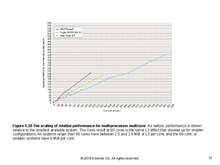
Figure 5. 30 The scaling of relative performance for multiprocessor multicore. As before, performance is shown relative to the smallest available system. The Xeon result at 80 cores is the same L 3 effect that showed up for smaller configurations. All systems larger than 80 cores have between 2. 5 and 3. 8 Mi. B of L 3 per core, and the 80 -core, or smaller, systems have 6 Mi. B per core. © 2019 Elsevier Inc. All rights reserved. 31

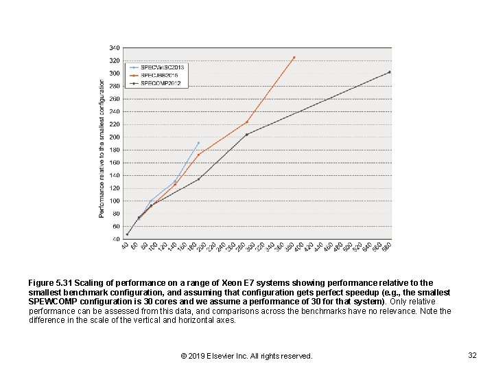
Figure 5. 31 Scaling of performance on a range of Xeon E 7 systems showing performance relative to the smallest benchmark configuration, and assuming that configuration gets perfect speedup (e. g. , the smallest SPEWCOMP configuration is 30 cores and we assume a performance of 30 for that system). Only relative performance can be assessed from this data, and comparisons across the benchmarks have no relevance. Note the difference in the scale of the vertical and horizontal axes. © 2019 Elsevier Inc. All rights reserved. 32

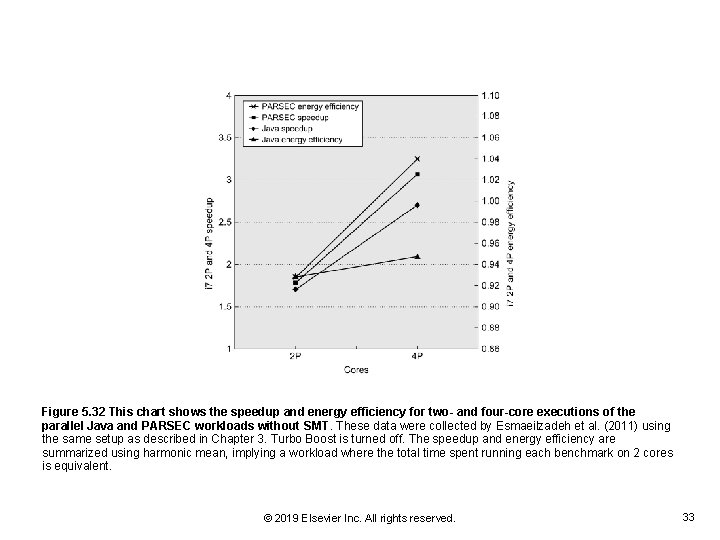
Figure 5. 32 This chart shows the speedup and energy efficiency for two- and four-core executions of the parallel Java and PARSEC workloads without SMT. These data were collected by Esmaeilzadeh et al. (2011) using the same setup as described in Chapter 3. Turbo Boost is turned off. The speedup and energy efficiency are summarized using harmonic mean, implying a workload where the total time spent running each benchmark on 2 cores is equivalent. © 2019 Elsevier Inc. All rights reserved. 33

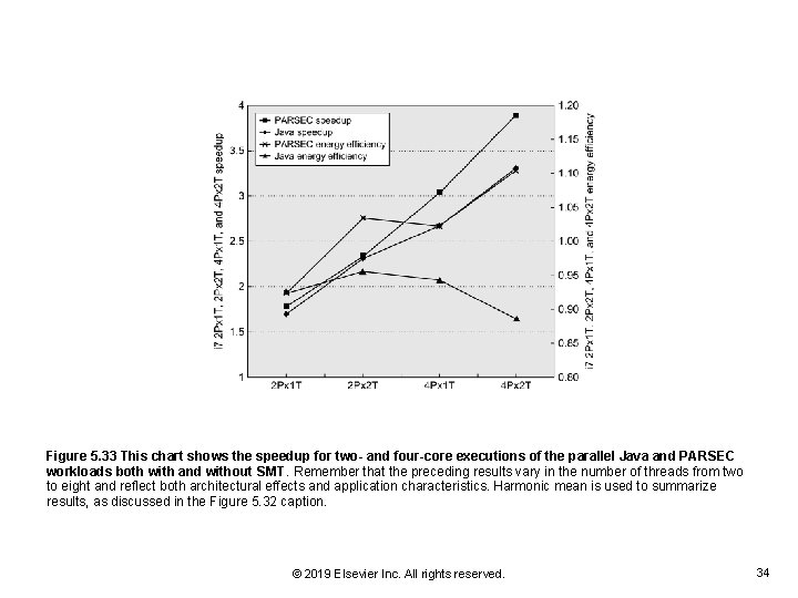
Figure 5. 33 This chart shows the speedup for two- and four-core executions of the parallel Java and PARSEC workloads both with and without SMT. Remember that the preceding results vary in the number of threads from two to eight and reflect both architectural effects and application characteristics. Harmonic mean is used to summarize results, as discussed in the Figure 5. 32 caption. © 2019 Elsevier Inc. All rights reserved. 34

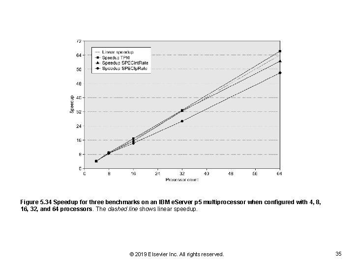
Figure 5. 34 Speedup for three benchmarks on an IBM e. Server p 5 multiprocessor when configured with 4, 8, 16, 32, and 64 processors. The dashed line shows linear speedup. © 2019 Elsevier Inc. All rights reserved. 35

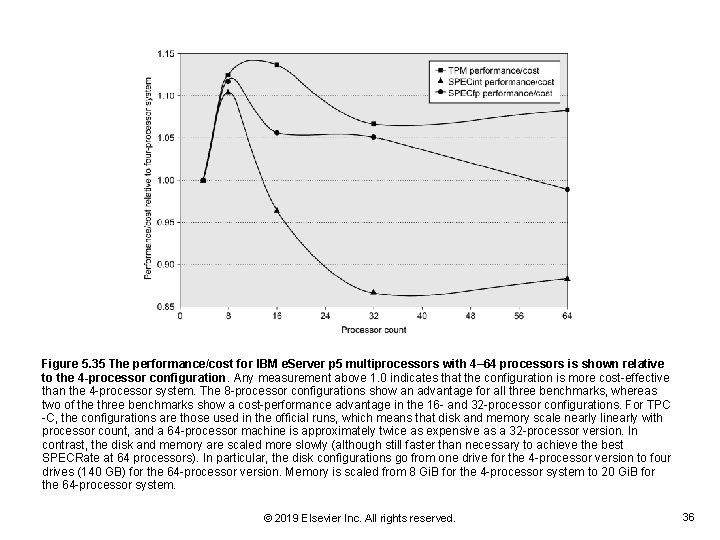
Figure 5. 35 The performance/cost for IBM e. Server p 5 multiprocessors with 4– 64 processors is shown relative to the 4 -processor configuration. Any measurement above 1. 0 indicates that the configuration is more cost-effective than the 4 -processor system. The 8 -processor configurations show an advantage for all three benchmarks, whereas two of the three benchmarks show a cost-performance advantage in the 16 - and 32 -processor configurations. For TPC -C, the configurations are those used in the official runs, which means that disk and memory scale nearly linearly with processor count, and a 64 -processor machine is approximately twice as expensive as a 32 -processor version. In contrast, the disk and memory are scaled more slowly (although still faster than necessary to achieve the best SPECRate at 64 processors). In particular, the disk configurations go from one drive for the 4 -processor version to four drives (140 GB) for the 64 -processor version. Memory is scaled from 8 Gi. B for the 4 -processor system to 20 Gi. B for the 64 -processor system. © 2019 Elsevier Inc. All rights reserved. 36

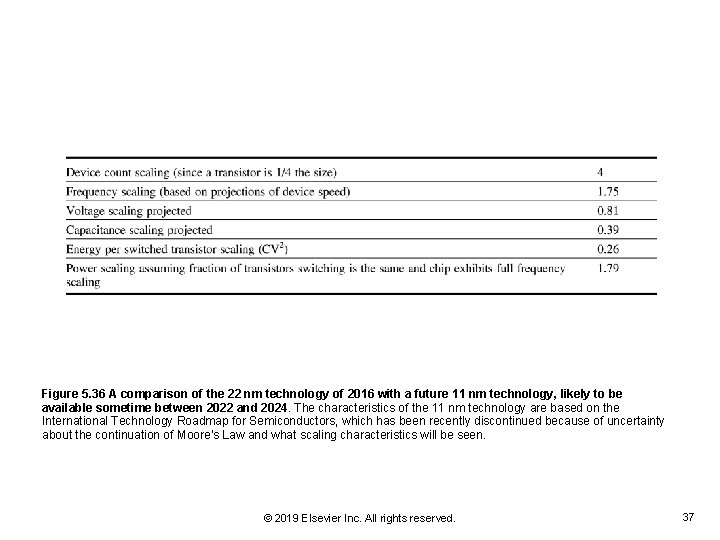
Figure 5. 36 A comparison of the 22 nm technology of 2016 with a future 11 nm technology, likely to be available sometime between 2022 and 2024. The characteristics of the 11 nm technology are based on the International Technology Roadmap for Semiconductors, which has been recently discontinued because of uncertainty about the continuation of Moore's Law and what scaling characteristics will be seen. © 2019 Elsevier Inc. All rights reserved. 37

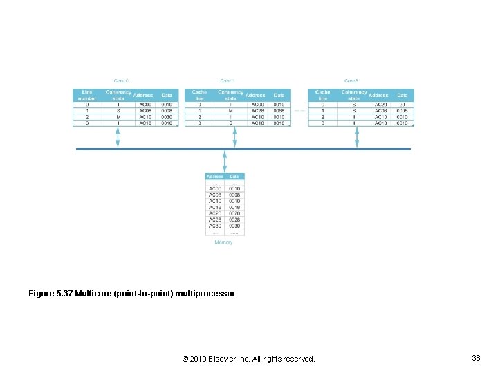
Figure 5. 37 Multicore (point-to-point) multiprocessor. © 2019 Elsevier Inc. All rights reserved. 38

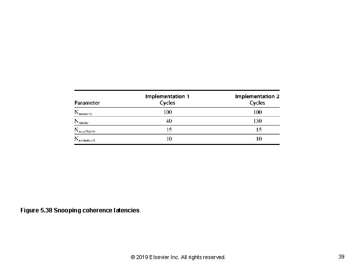
Figure 5. 38 Snooping coherence latencies. © 2019 Elsevier Inc. All rights reserved. 39

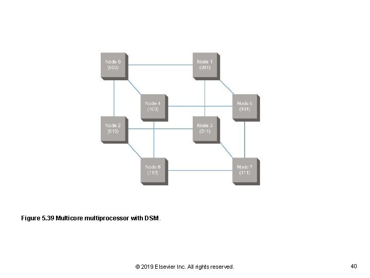
Figure 5. 39 Multicore multiprocessor with DSM. © 2019 Elsevier Inc. All rights reserved. 40

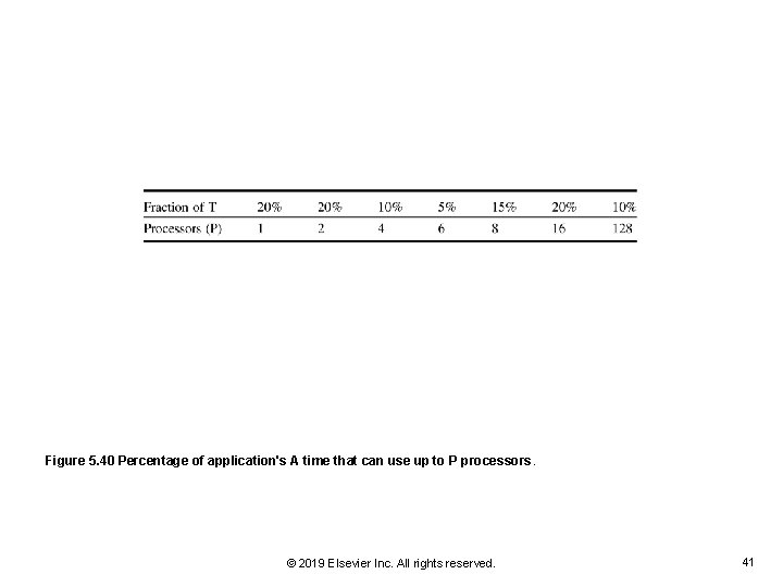
Figure 5. 40 Percentage of application's A time that can use up to P processors. © 2019 Elsevier Inc. All rights reserved. 41