Chapter 5 Synchronous Sequential Logic Part 1 Origionally

- Slides: 25

Chapter 5: Synchronous Sequential Logic – Part 1 Origionally By Reham S. Al-Majed Imam Muhammad Bin Saud University

Outline q Introduction. q Sequential Circuits � Types of SC. q Latches q Flip flops SR FF. � D FF. � JK FF. � T FF. � 2

Introduction q The circuits considered thus far have been combinational � q The output depends only on the current inputs. Most systems in practice include storage elements. � Sequential logic. 3

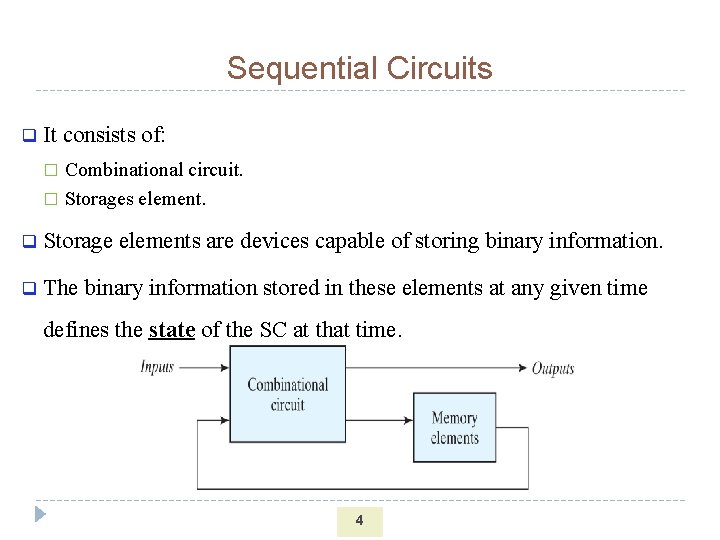
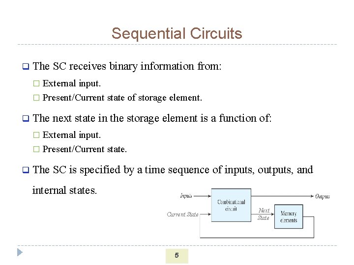
Sequential Circuits q It consists of: Combinational circuit. � Storages element. � q Storage elements are devices capable of storing binary information. q The binary information stored in these elements at any given time defines the state of the SC at that time. 4

Sequential Circuits q The SC receives binary information from: External input. � Present/Current state of storage element. � q The next state in the storage element is a function of: External input. � Present/Current state. � q The SC is specified by a time sequence of inputs, outputs, and internal states. Current State 5 Next State

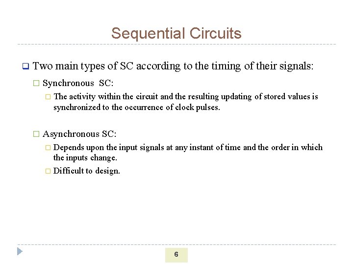
Sequential Circuits q Two main types of SC according to the timing of their signals: � Synchronous SC: � The activity within the circuit and the resulting updating of stored values is synchronized to the occurrence of clock pulses. � Asynchronous SC: � Depends upon the input signals at any instant of time and the order in which the inputs change. � Difficult to design. 6

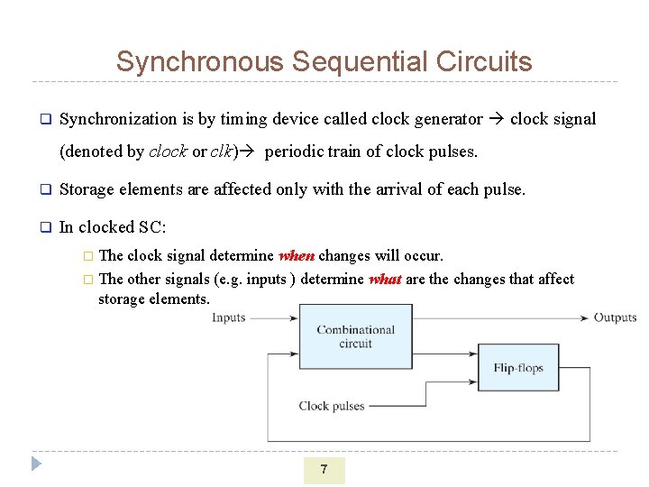
Synchronous Sequential Circuits q Synchronization is by timing device called clock generator clock signal (denoted by clock or clk) periodic train of clock pulses. q Storage elements are affected only with the arrival of each pulse. q In clocked SC: � The clock signal determine when changes will occur. � The other signals (e. g. inputs ) determine what are the changes that affect storage elements. 7

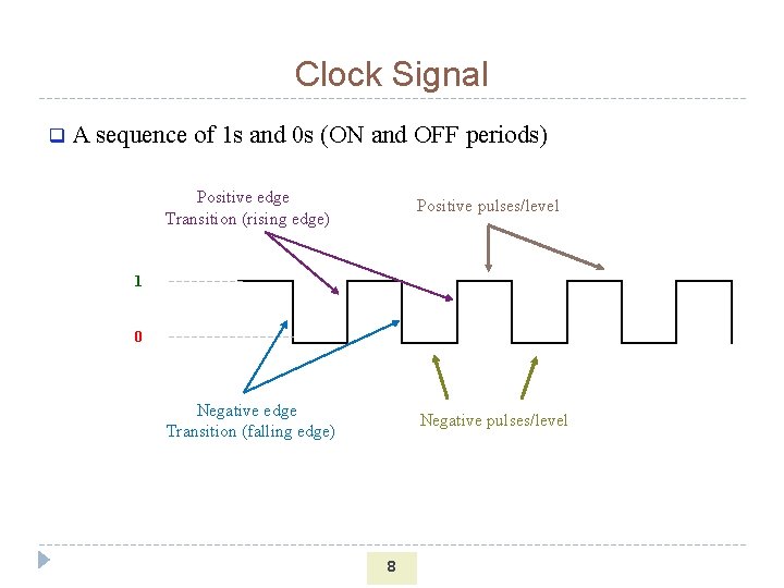
Clock Signal q A sequence of 1 s and 0 s (ON and OFF periods) Positive edge Transition (rising edge) Positive pulses/level Negative edge Transition (falling edge) Negative pulses/level 1 0 8

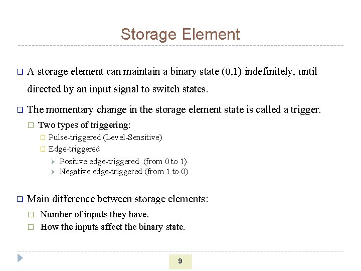
Storage Element q A storage element can maintain a binary state (0, 1) indefinitely, until directed by an input signal to switch states. q The momentary change in the storage element state is called a trigger. � Two types of triggering: Pulse-triggered (Level-Sensitive) � Edge-triggered Ø Positive edge-triggered (from 0 to 1) Ø Negative edge-triggered (from 1 to 0) � q Main difference between storage elements: � � Number of inputs they have. How the inputs affect the binary state. 9

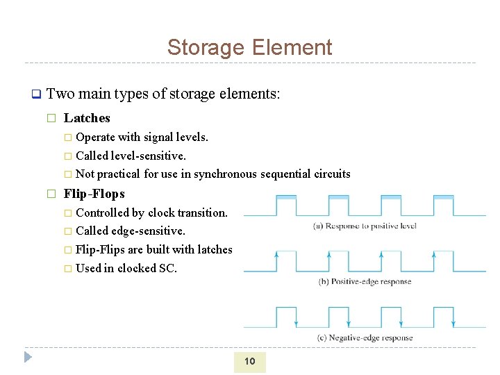
Storage Element q Two main types of storage elements: � Latches � Operate with signal levels. � Called level-sensitive. � Not practical for use in synchronous sequential circuits � Flip-Flops � Controlled by clock transition. � Called edge-sensitive. � Flip-Flips are built with latches � Used in clocked SC. 10

Latches q A latch is binary storage element � Can store a 0 or 1 q It is the most basic storage element. q It is easy to build. q The trigger of a latch start as soon as the clock pulse changes to the logic-1 level. q The new state of a latch appears at the output while the pulse is still active. q Latches respond to new input values as clock pulse is still at logic-1 level. 11

q Latch circuits are not suitable in synchronous logic circuits. � q Any change in the excitation input immediately causes a change in the latch output. This leads to the edge-triggered memory elements, called flipflops. Output transitions occur at a specific level of the clock pulse � Otherwise, the ff is unresponsive to further changes until the clock pulse returns to 0 and another pulse occurs � 12

Flip-Flop q q A FF is a binary storage element that can store 0 or 1 a FF maintains a binary state until directed by a clock pulse to switch states q The most common types of FFs are SR, D, JK, and T. 13

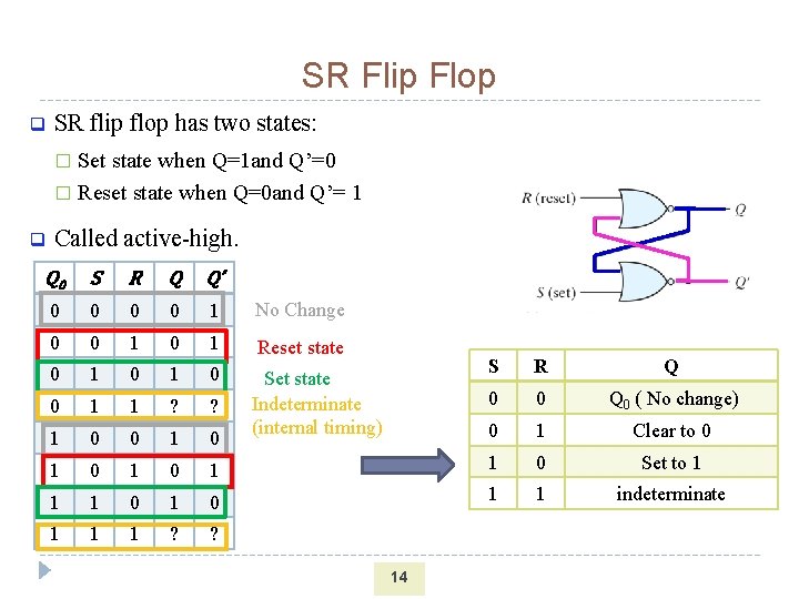
SR Flip Flop q SR flip flop has two states: Set state when Q=1 and Q’=0 � Reset state when Q=0 and Q’= 1 � q Called active-high. Q 0 S R Q Q’ 0 0 1 No Change 0 0 1 Reset state 0 1 0 0 1 1 ? ? 1 0 0 1 0 1 1 1 S R Q 0 0 Q 0 ( No change) 0 1 Clear to 0 1 1 0 Set to 1 1 0 1 1 indeterminate ? ? Set state Indeterminate (internal timing) 14

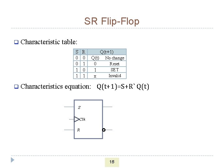
SR Flip-Flop q Characteristic table: S 0 0 1 1 q R 0 1 Q(t+1) Q(t) 0 1 x No change Reset SET Invalid Characteristics equation: Q(t+1)=S+R` Q(t) S Clk R 15

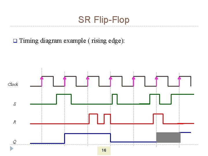
SR Flip-Flop q Timing diagram example ( rising edge): Clock S R Q 16

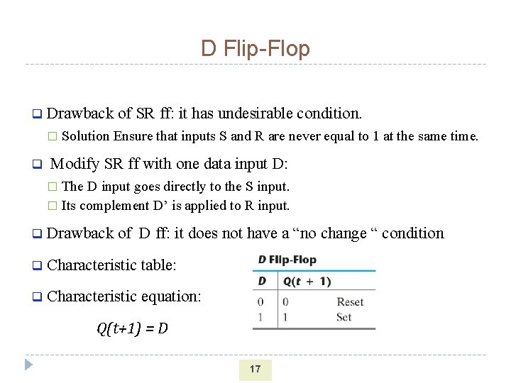
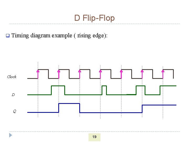
D Flip-Flop q Drawback of SR ff: it has undesirable condition. � q Solution Ensure that inputs S and R are never equal to 1 at the same time. Modify SR ff with one data input D: The D input goes directly to the S input. � Its complement D’ is applied to R input. � q Drawback of D ff: it does not have a “no change “ condition q Characteristic table: q Characteristic equation: Q(t+1) = D 17

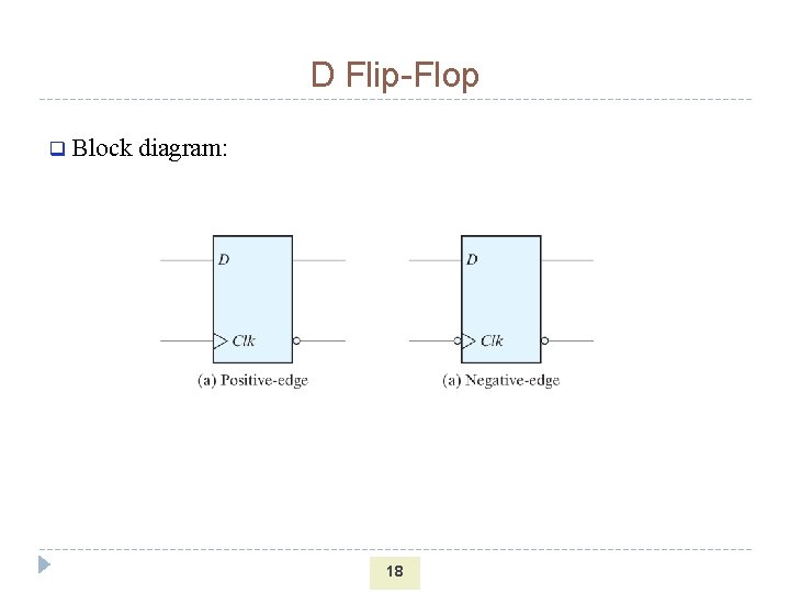
D Flip-Flop q Block diagram: 18

D Flip-Flop q Timing diagram example ( rising edge): Clock D Q 19

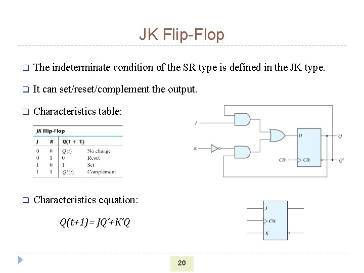
JK Flip-Flop q The indeterminate condition of the SR type is defined in the JK type. q It can set/reset/complement the output. q Characteristics table: q Characteristics equation: Q(t+1)= JQ’+K’Q 20

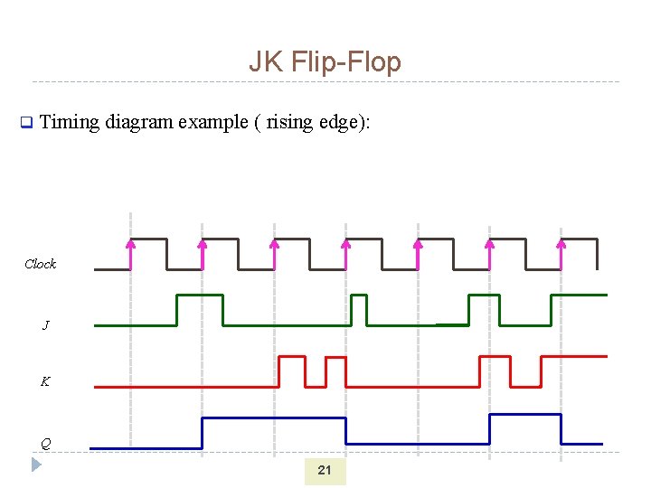
JK Flip-Flop q Timing diagram example ( rising edge): Clock J K Q 21

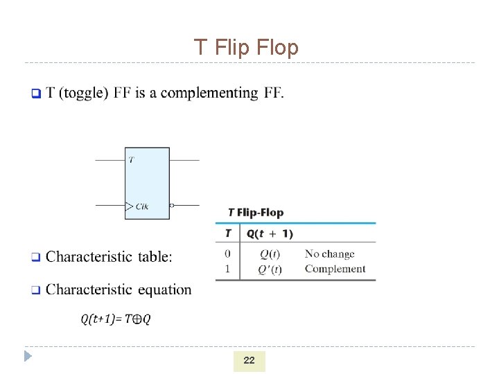
T Flip Flop q ×ﺥ 22

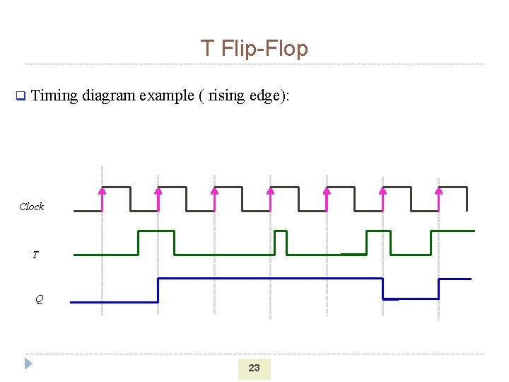
T Flip-Flop q Timing diagram example ( rising edge): Clock T Q 23

Direct Inputs q Flip Flops will sometimes provide special input terminals for setting or clearing the FF asynchronously. � Direct inputs force FF to a state independently of clock. q The input that sets FF to 1 is called preset or direct set. q The input that resets FF to 0 is called clear or direct reset. q These inputs are useful for bringing the FFs to an initial state prior to its clocked operation. 24

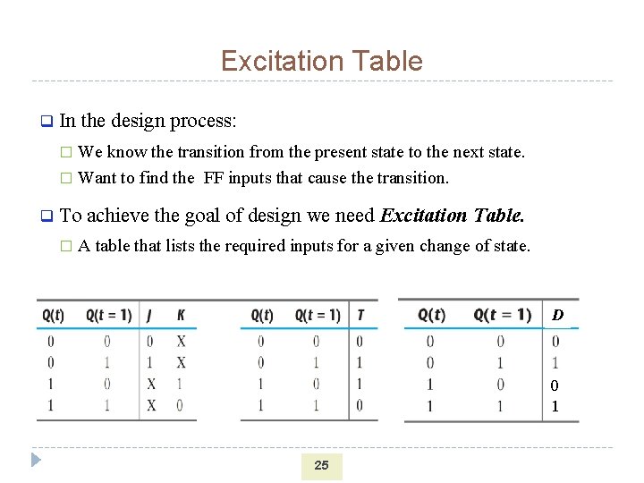
Excitation Table q In the design process: We know the transition from the present state to the next state. � Want to find the FF inputs that cause the transition. � q To achieve the goal of design we need Excitation Table. � A table that lists the required inputs for a given change of state. D 0 1 25