Chapter 5 STM 32 Arm Timer Programming STM
![Bits 2 y: 2 y+1 MODERy[1: 0]: Port x configuration bits (y = 0. Bits 2 y: 2 y+1 MODERy[1: 0]: Port x configuration bits (y = 0.](https://slidetodoc.com/presentation_image_h2/794263eff010516aa5cb0750a1c17661/image-37.jpg)
- Slides: 50

Chapter 5: STM 32 Arm Timer Programming STM 32 F 0 Arm Cortex M 0 Programming for Embedded Systems Using C Language with STM 32 F 0 Nucleo Board by Mazidi, et al. www. microdigitaled. com

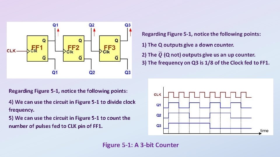
Regarding Figure 5 -1, notice the following points: 4) We can use the circuit in Figure 5 -1 to divide clock frequency. 5) We can use the circuit in Figure 5 -1 to count the number of pulses fed to CLK pin of FF 1. Figure 5 -1: A 3 -bit Counter

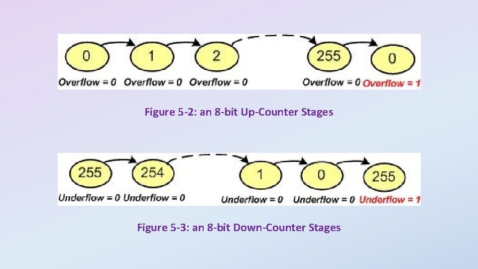
Figure 5 -2: an 8 -bit Up-Counter Stages Figure 5 -3: an 8 -bit Down-Counter Stages

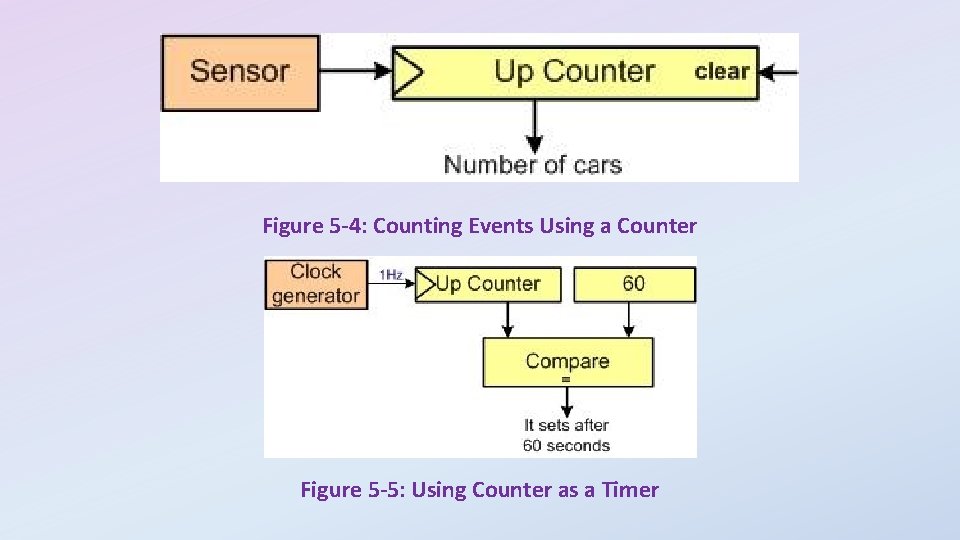
Figure 5 -4: Counting Events Using a Counter Figure 5 -5: Using Counter as a Timer

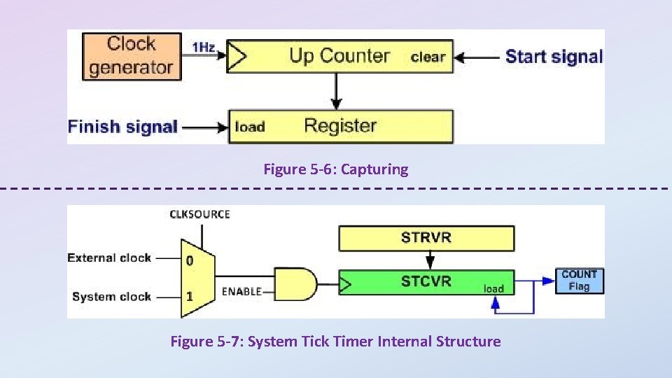
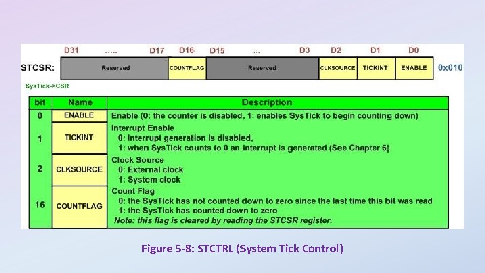
Figure 5 -6: Capturing Figure 5 -7: System Tick Timer Internal Structure

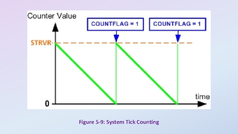
Figure 5 -8: STCTRL (System Tick Control)

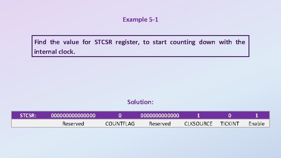
Figure 5 -9: System Tick Counting

Example 5 -1 Find the value for STCSR register, to start counting down with the internal clock. Solution: STCSR: 00000000 Reserved 0 0000000 1 COUNTFLAG Reserved CLKSOURCE 0 TICKINT 1 Enable

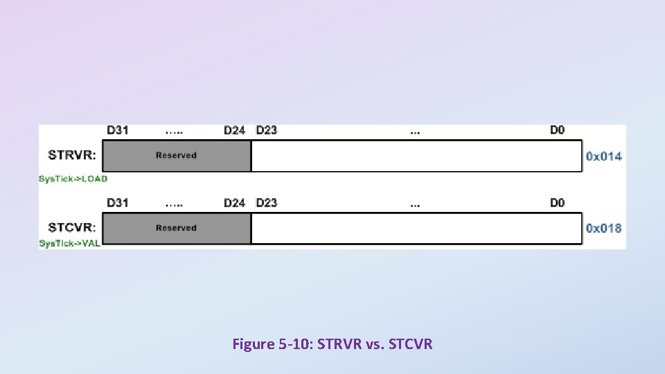
Figure 5 -10: STRVR vs. STCVR

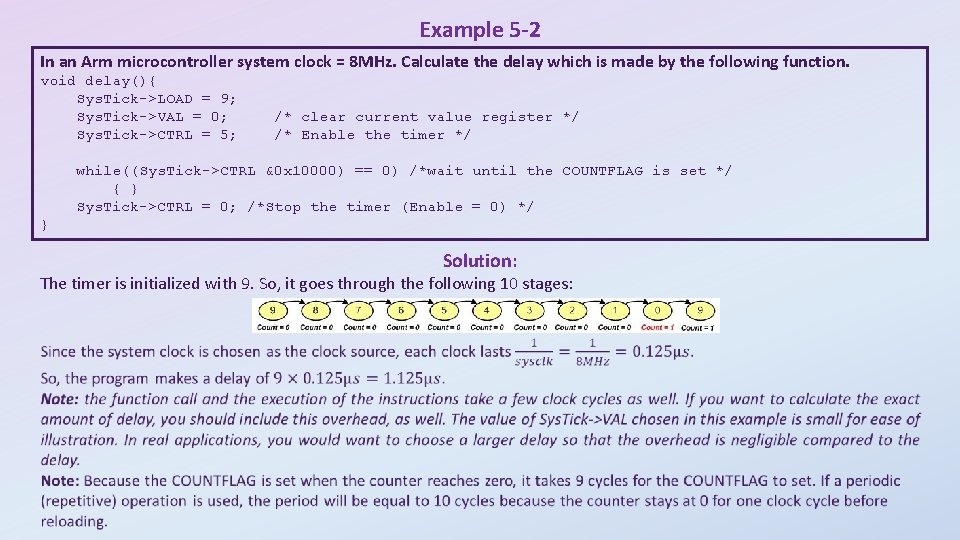
Example 5 -2 In an Arm microcontroller system clock = 8 MHz. Calculate the delay which is made by the following function. void delay(){ Sys. Tick->LOAD = 9; Sys. Tick->VAL = 0; Sys. Tick->CTRL = 5; /* clear current value register */ /* Enable the timer */ while((Sys. Tick->CTRL &0 x 10000) == 0) /*wait until the COUNTFLAG is set */ { } Sys. Tick->CTRL = 0; /*Stop the timer (Enable = 0) */ } Solution: The timer is initialized with 9. So, it goes through the following 10 stages:

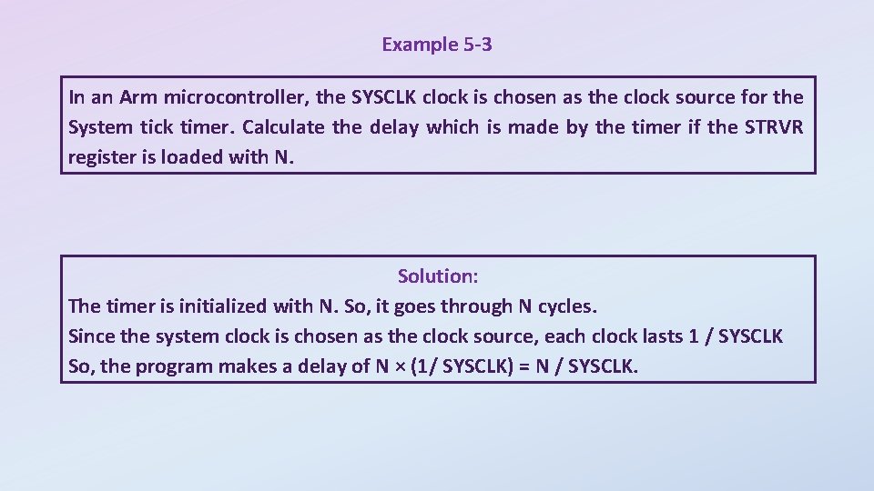
Example 5 -3 In an Arm microcontroller, the SYSCLK clock is chosen as the clock source for the System tick timer. Calculate the delay which is made by the timer if the STRVR register is loaded with N. Solution: The timer is initialized with N. So, it goes through N cycles. Since the system clock is chosen as the clock source, each clock lasts 1 / SYSCLK So, the program makes a delay of N × (1/ SYSCLK) = N / SYSCLK.

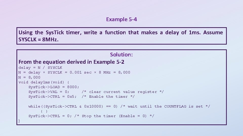
Example 5 -4 Using the Sys. Tick timer, write a function that makes a delay of 1 ms. Assume SYSCLK = 8 MHz. Solution: From the equation derived in Example 5 -2 delay = N / SYSCLK N = delay × SYSCLK = 0. 001 sec × 8 MHz = 8, 000 N = 8, 000 void delay 1 ms(void) { Sys. Tick->LOAD = 8000; Sys. Tick->VAL = 0; /* clear current value register */ Sys. Tick->CTRL = 0 x 5; /* Enable the timer */ while((Sys. Tick->CTRL & 0 x 10000) == 0) /* wait until the COUNTFLAG is set */ { } Sys. Tick->CTRL = 0; /* Stop the timer (Enable = 0) */ }

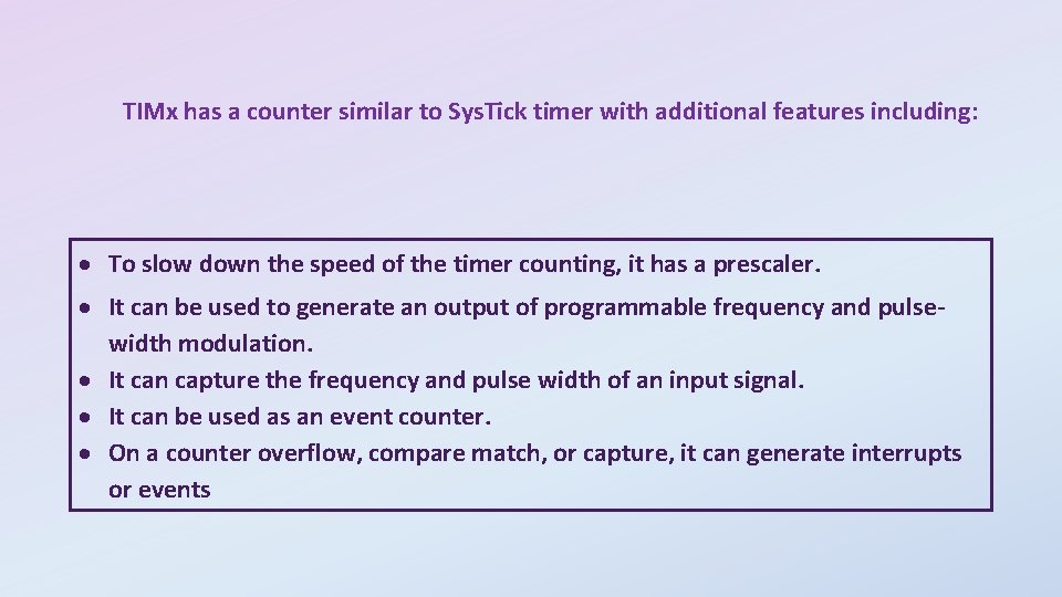
TIMx has a counter similar to Sys. Tick timer with additional features including: To slow down the speed of the timer counting, it has a prescaler. It can be used to generate an output of programmable frequency and pulsewidth modulation. It can capture the frequency and pulse width of an input signal. It can be used as an event counter. On a counter overflow, compare match, or capture, it can generate interrupts or events

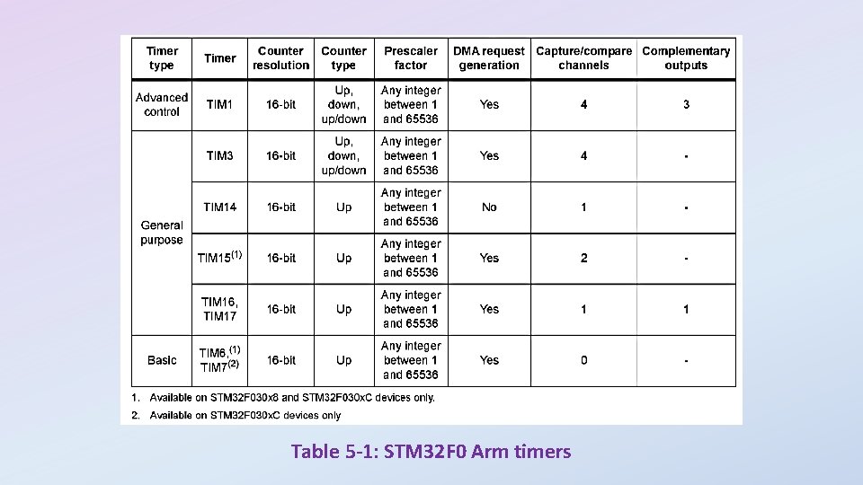
Table 5 -1: STM 32 F 0 Arm timers

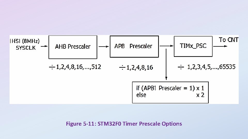
Figure 5 -11: STM 32 F 0 Timer Prescale Options

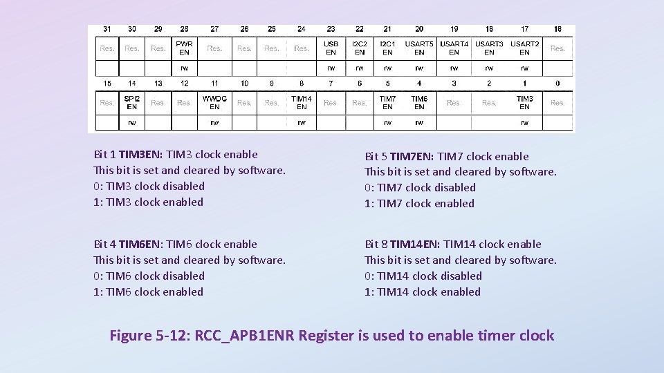
Bit 1 TIM 3 EN: TIM 3 clock enable This bit is set and cleared by software. 0: TIM 3 clock disabled 1: TIM 3 clock enabled Bit 5 TIM 7 EN: TIM 7 clock enable This bit is set and cleared by software. 0: TIM 7 clock disabled 1: TIM 7 clock enabled Bit 4 TIM 6 EN: TIM 6 clock enable This bit is set and cleared by software. 0: TIM 6 clock disabled 1: TIM 6 clock enabled Bit 8 TIM 14 EN: TIM 14 clock enable This bit is set and cleared by software. 0: TIM 14 clock disabled 1: TIM 14 clock enabled Figure 5 -12: RCC_APB 1 ENR Register is used to enable timer clock

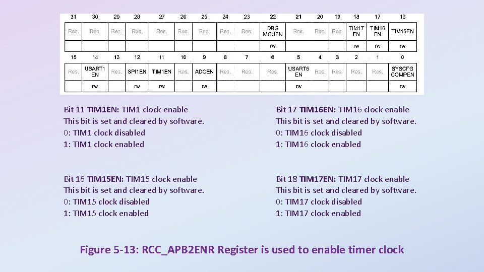
Bit 11 TIM 1 EN: TIM 1 clock enable This bit is set and cleared by software. 0: TIM 1 clock disabled 1: TIM 1 clock enabled Bit 17 TIM 16 EN: TIM 16 clock enable This bit is set and cleared by software. 0: TIM 16 clock disabled 1: TIM 16 clock enabled Bit 16 TIM 15 EN: TIM 15 clock enable This bit is set and cleared by software. 0: TIM 15 clock disabled 1: TIM 15 clock enabled Bit 18 TIM 17 EN: TIM 17 clock enable This bit is set and cleared by software. 0: TIM 17 clock disabled 1: TIM 17 clock enabled Figure 5 -13: RCC_APB 2 ENR Register is used to enable timer clock

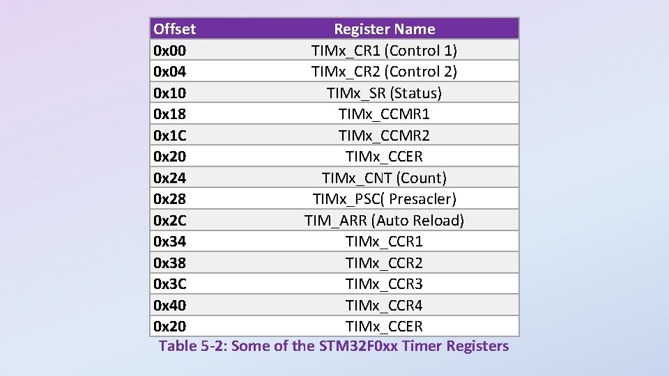
Offset Register Name 0 x 00 TIMx_CR 1 (Control 1) 0 x 04 TIMx_CR 2 (Control 2) 0 x 10 TIMx_SR (Status) 0 x 18 TIMx_CCMR 1 0 x 1 C TIMx_CCMR 2 0 x 20 TIMx_CCER 0 x 24 TIMx_CNT (Count) 0 x 28 TIMx_PSC( Presacler) 0 x 2 C TIM_ARR (Auto Reload) 0 x 34 TIMx_CCR 1 0 x 38 TIMx_CCR 2 0 x 3 C TIMx_CCR 3 0 x 40 TIMx_CCR 4 0 x 20 TIMx_CCER Table 5 -2: Some of the STM 32 F 0 xx Timer Registers

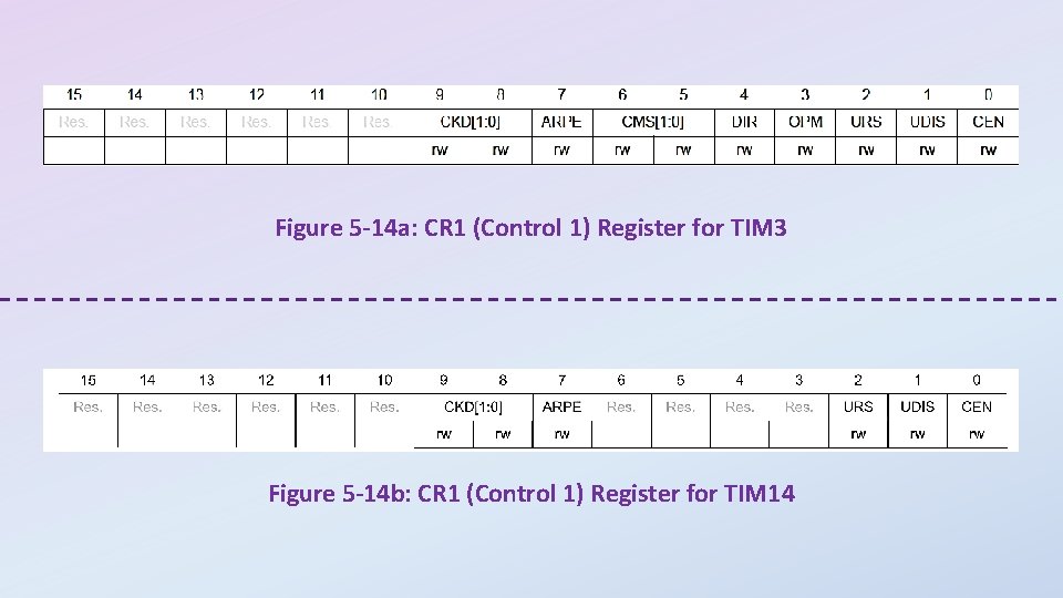
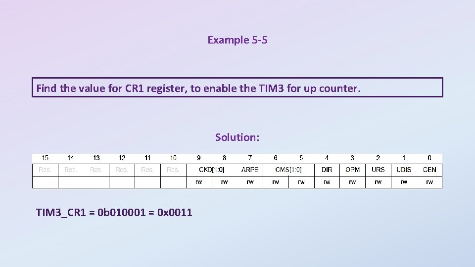
Figure 5 -14 a: CR 1 (Control 1) Register for TIM 3 Figure 5 -14 b: CR 1 (Control 1) Register for TIM 14

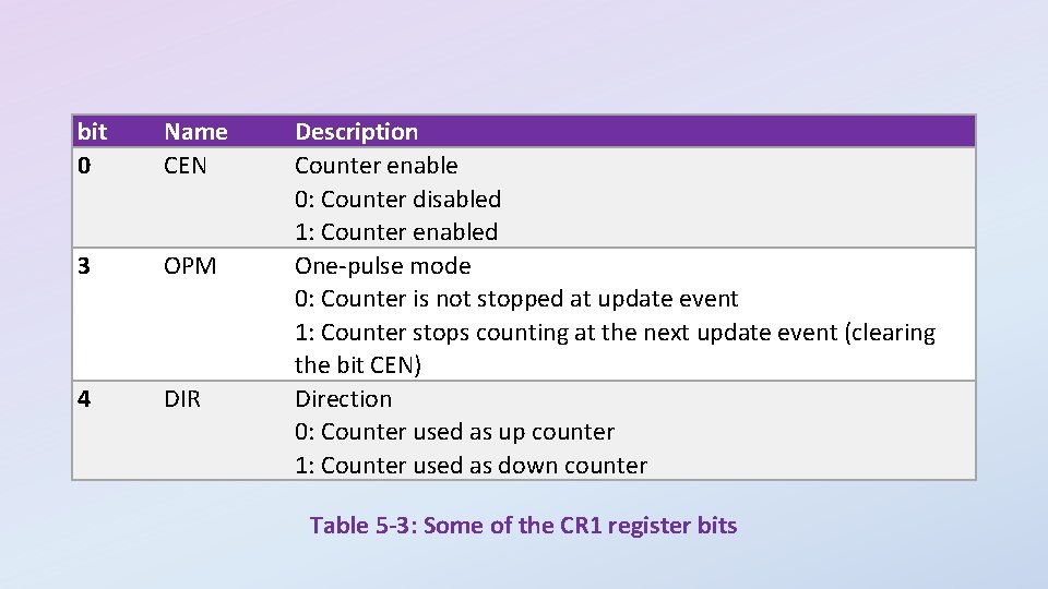
bit 0 Name CEN 3 OPM 4 DIR Description Counter enable 0: Counter disabled 1: Counter enabled One-pulse mode 0: Counter is not stopped at update event 1: Counter stops counting at the next update event (clearing the bit CEN) Direction 0: Counter used as up counter 1: Counter used as down counter Table 5 -3: Some of the CR 1 register bits

Example 5 -5 Find the value for CR 1 register, to enable the TIM 3 for up counter. Solution: TIM 3_CR 1 = 0 b 010001 = 0 x 0011

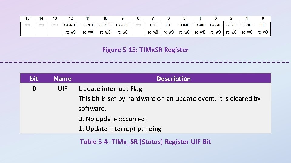
Figure 5 -15: TIMx. SR Register bit 0 Name Description UIF Update interrupt Flag This bit is set by hardware on an update event. It is cleared by software. 0: No update occurred. 1: Update interrupt pending Table 5 -4: TIMx_SR (Status) Register UIF Bit

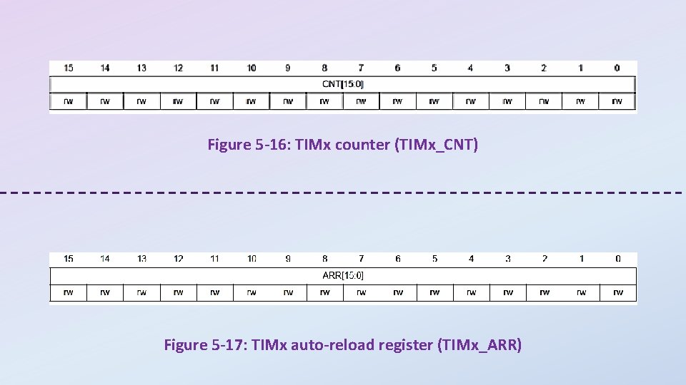
Figure 5 -16: TIMx counter (TIMx_CNT) Figure 5 -17: TIMx auto-reload register (TIMx_ARR)

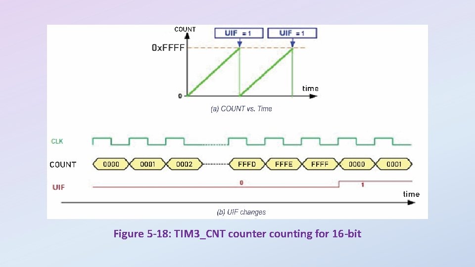
Figure 5 -18: TIM 3_CNT counter counting for 16 -bit

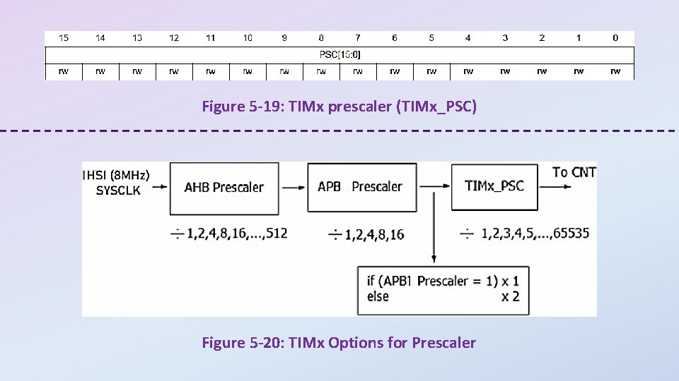
Figure 5 -19: TIMx prescaler (TIMx_PSC) Figure 5 -20: TIMx Options for Prescaler

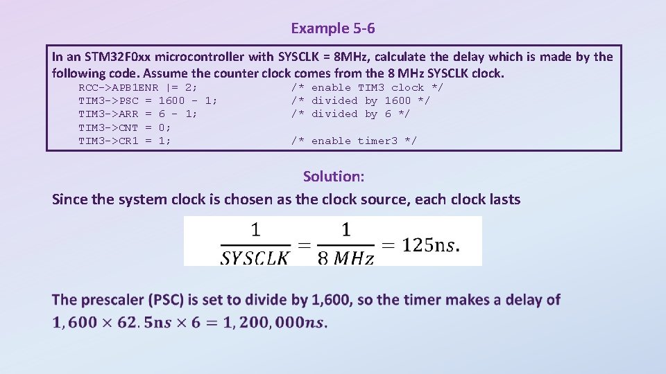
Example 5 -6 In an STM 32 F 0 xx microcontroller with SYSCLK = 8 MHz, calculate the delay which is made by the following code. Assume the counter clock comes from the 8 MHz SYSCLK clock. RCC->APB 1 ENR |= 2; TIM 3 ->PSC = 1600 - 1; TIM 3 ->ARR = 6 - 1; TIM 3 ->CNT = 0; TIM 3 ->CR 1 = 1; /* enable TIM 3 clock */ /* divided by 1600 */ /* divided by 6 */ /* enable timer 3 */ Solution: Since the system clock is chosen as the clock source, each clock lasts

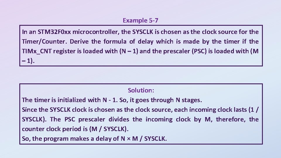
Example 5 -7 In an STM 32 F 0 xx microcontroller, the SYSCLK is chosen as the clock source for the Timer/Counter. Derive the formula of delay which is made by the timer if the TIMx_CNT register is loaded with (N – 1) and the prescaler (PSC) is loaded with (M – 1). Solution: The timer is initialized with N - 1. So, it goes through N stages. Since the SYSCLK clock is chosen as the clock source, each incoming clock lasts (1 / SYSCLK). The PSC prescaler divides the incoming clock by M, therefore, the counter clock period is (M / SYSCLK). So, the program makes a delay of N × M / SYSCLK.

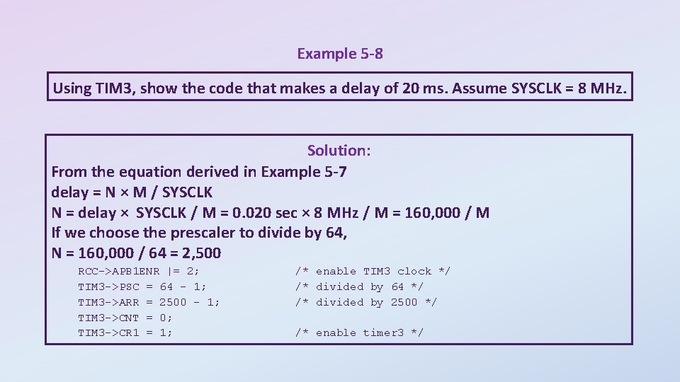
Example 5 -8 Using TIM 3, show the code that makes a delay of 20 ms. Assume SYSCLK = 8 MHz. Solution: From the equation derived in Example 5 -7 delay = N × M / SYSCLK N = delay × SYSCLK / M = 0. 020 sec × 8 MHz / M = 160, 000 / M If we choose the prescaler to divide by 64, N = 160, 000 / 64 = 2, 500 RCC->APB 1 ENR |= 2; TIM 3 ->PSC = 64 - 1; TIM 3 ->ARR = 2500 - 1; TIM 3 ->CNT = 0; TIM 3 ->CR 1 = 1; /* enable TIM 3 clock */ /* divided by 64 */ /* divided by 2500 */ /* enable timer 3 */

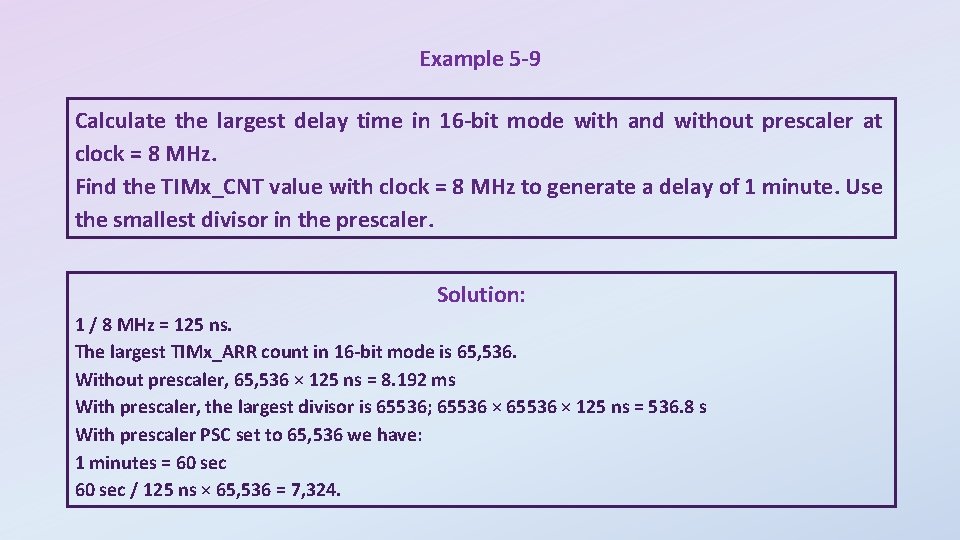
Example 5 -9 Calculate the largest delay time in 16 -bit mode with and without prescaler at clock = 8 MHz. Find the TIMx_CNT value with clock = 8 MHz to generate a delay of 1 minute. Use the smallest divisor in the prescaler. Solution: 1 / 8 MHz = 125 ns. The largest TIMx_ARR count in 16 -bit mode is 65, 536. Without prescaler, 65, 536 × 125 ns = 8. 192 ms With prescaler, the largest divisor is 65536; 65536 × 125 ns = 536. 8 s With prescaler PSC set to 65, 536 we have: 1 minutes = 60 sec / 125 ns × 65, 536 = 7, 324.

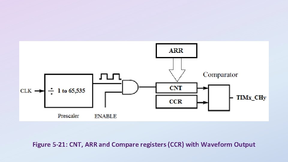
Figure 5 -21: CNT, ARR and Compare registers (CCR) with Waveform Output

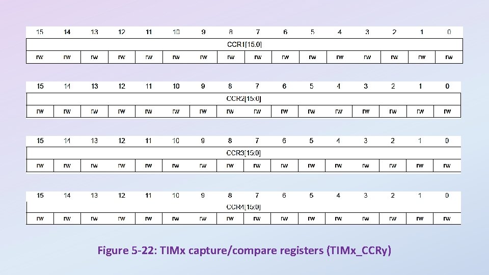
Figure 5 -22: TIMx capture/compare registers (TIMx_CCRy)

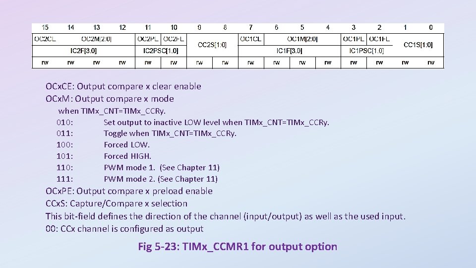
OCx. CE: Output compare x clear enable OCx. M: Output compare x mode when TIMx_CNT=TIMx_CCRy. 010: Set output to inactive LOW level when TIMx_CNT=TIMx_CCRy. 011: Toggle when TIMx_CNT=TIMx_CCRy. 100: Forced LOW. 101: Forced HIGH. 110: PWM mode 1. (See Chapter 11) 111: PWM mode 2. (See Chapter 11) OCx. PE: Output compare x preload enable CCx. S: Capture/Compare x selection This bit-field defines the direction of the channel (input/output) as well as the used input. 00: CCx channel is configured as output Fig 5 -23: TIMx_CCMR 1 for output option

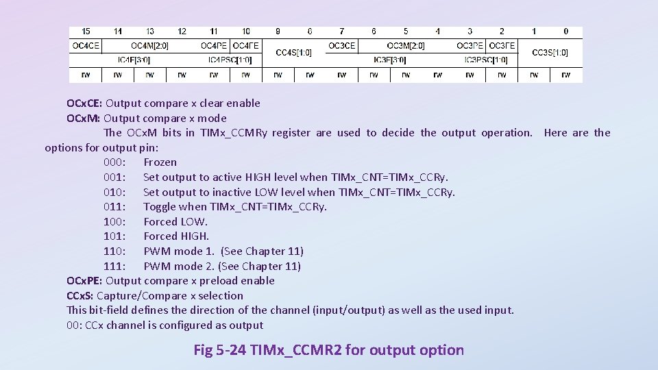
OCx. CE: Output compare x clear enable OCx. M: Output compare x mode The OCx. M bits in TIMx_CCMRy register are used to decide the output operation. Here are the options for output pin: 000: Frozen 001: Set output to active HIGH level when TIMx_CNT=TIMx_CCRy. 010: Set output to inactive LOW level when TIMx_CNT=TIMx_CCRy. 011: Toggle when TIMx_CNT=TIMx_CCRy. 100: Forced LOW. 101: Forced HIGH. 110: PWM mode 1. (See Chapter 11) 111: PWM mode 2. (See Chapter 11) OCx. PE: Output compare x preload enable CCx. S: Capture/Compare x selection This bit-field defines the direction of the channel (input/output) as well as the used input. 00: CCx channel is configured as output Fig 5 -24 TIMx_CCMR 2 for output option

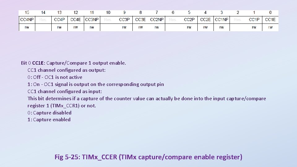
Bit 0 CC 1 E: Capture/Compare 1 output enable. CC 1 channel configured as output: 0: Off - OC 1 is not active 1: On - OC 1 signal is output on the corresponding output pin CC 1 channel configured as input: This bit determines if a capture of the counter value can actually be done into the input capture/compare register 1 (TIMx_CCR 1) or not. 0: Capture disabled 1: Capture enabled Fig 5 -25: TIMx_CCER (TIMx capture/compare enable register)

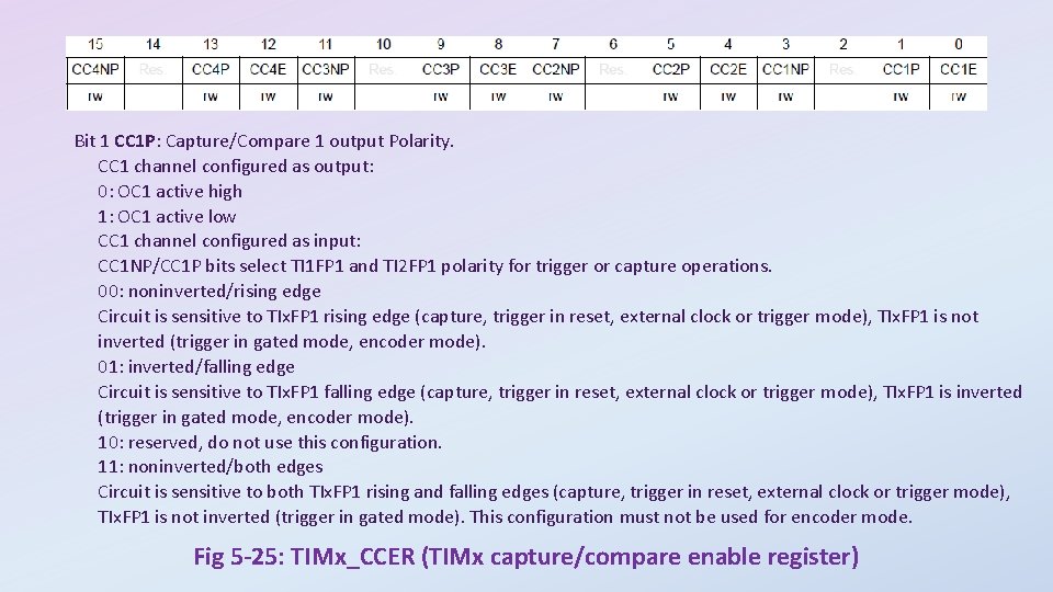
Bit 1 CC 1 P: Capture/Compare 1 output Polarity. CC 1 channel configured as output: 0: OC 1 active high 1: OC 1 active low CC 1 channel configured as input: CC 1 NP/CC 1 P bits select TI 1 FP 1 and TI 2 FP 1 polarity for trigger or capture operations. 00: noninverted/rising edge Circuit is sensitive to TIx. FP 1 rising edge (capture, trigger in reset, external clock or trigger mode), TIx. FP 1 is not inverted (trigger in gated mode, encoder mode). 01: inverted/falling edge Circuit is sensitive to TIx. FP 1 falling edge (capture, trigger in reset, external clock or trigger mode), TIx. FP 1 is inverted (trigger in gated mode, encoder mode). 10: reserved, do not use this configuration. 11: noninverted/both edges Circuit is sensitive to both TIx. FP 1 rising and falling edges (capture, trigger in reset, external clock or trigger mode), TIx. FP 1 is not inverted (trigger in gated mode). This configuration must not be used for encoder mode. Fig 5 -25: TIMx_CCER (TIMx capture/compare enable register)

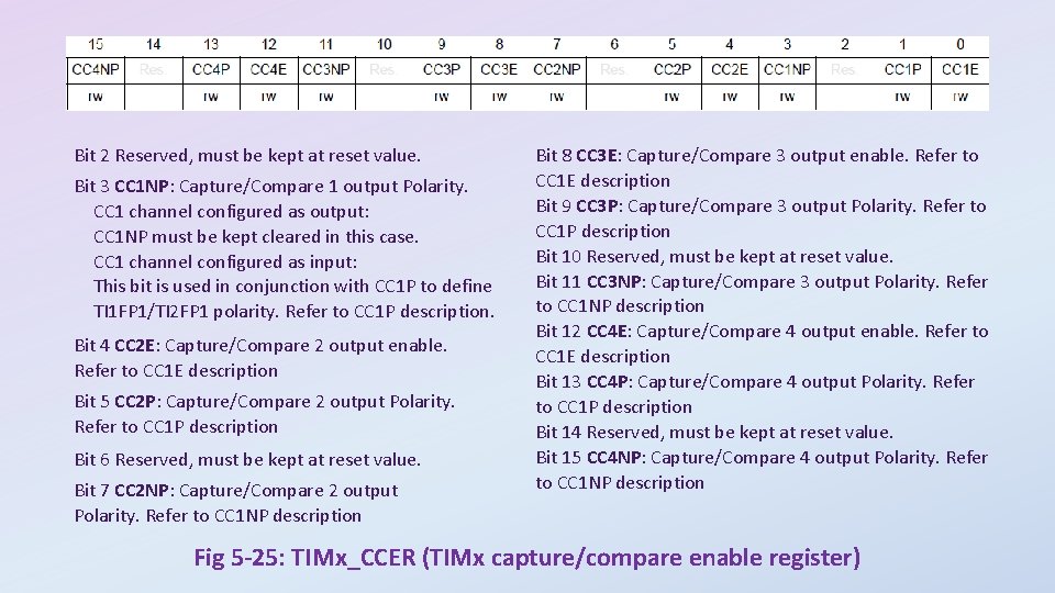
Bit 2 Reserved, must be kept at reset value. Bit 3 CC 1 NP: Capture/Compare 1 output Polarity. CC 1 channel configured as output: CC 1 NP must be kept cleared in this case. CC 1 channel configured as input: This bit is used in conjunction with CC 1 P to define TI 1 FP 1/TI 2 FP 1 polarity. Refer to CC 1 P description. Bit 4 CC 2 E: Capture/Compare 2 output enable. Refer to CC 1 E description Bit 5 CC 2 P: Capture/Compare 2 output Polarity. Refer to CC 1 P description Bit 6 Reserved, must be kept at reset value. Bit 7 CC 2 NP: Capture/Compare 2 output Polarity. Refer to CC 1 NP description Bit 8 CC 3 E: Capture/Compare 3 output enable. Refer to CC 1 E description Bit 9 CC 3 P: Capture/Compare 3 output Polarity. Refer to CC 1 P description Bit 10 Reserved, must be kept at reset value. Bit 11 CC 3 NP: Capture/Compare 3 output Polarity. Refer to CC 1 NP description Bit 12 CC 4 E: Capture/Compare 4 output enable. Refer to CC 1 E description Bit 13 CC 4 P: Capture/Compare 4 output Polarity. Refer to CC 1 P description Bit 14 Reserved, must be kept at reset value. Bit 15 CC 4 NP: Capture/Compare 4 output Polarity. Refer to CC 1 NP description Fig 5 -25: TIMx_CCER (TIMx capture/compare enable register)
![Bits 2 y 2 y1 MODERy1 0 Port x configuration bits y 0 Bits 2 y: 2 y+1 MODERy[1: 0]: Port x configuration bits (y = 0.](https://slidetodoc.com/presentation_image_h2/794263eff010516aa5cb0750a1c17661/image-37.jpg)
Bits 2 y: 2 y+1 MODERy[1: 0]: Port x configuration bits (y = 0. . 15) These bits are written by software to configure the I/O direction mode. 00: Input (reset state) 01: General purpose output mode 10: Alternate function mode 11: Analog mode Figure 5 -26: MODER Register is used to select alternative pin functions

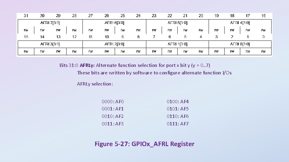
Bits 31: 0 AFRLy: Alternate function selection for port x bit y (y = 0. . 7) These bits are written by software to configure alternate function I/Os AFRLy selection: 0000: AF 0 0001: AF 1 0010: AF 2 0011: AF 3 0100: AF 4 0101: AF 5 0110: AF 6 0111: AF 7 Figure 5 -27: GPIOx_AFRL Register

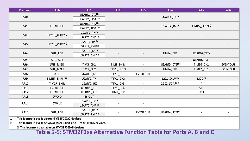
1. 2. Pin name AF 0 SPI 1_SCK SPI 1_MISO AF 1 USART 1_CTS(2) USART 2_CTS(1)(3) USART 1_RTS(2) USART 2_RTS(1)(3) USART 1_TX(2) USART 2_TX(1)(3) USART 1_RX(2) USART 2_RX(1)(3) USART 1_CK(2) USART 2_CK(1)(3) TIM 3_CH 1 AF 2 AF 3 AF 4 AF 5 AF 6 PA 0 - - - USART 4_TX(1) - - PA 1 EVENTOUT - - USART 4_RX(1) TIM 15_CH 1 N(1) - PA 2 TIM 15_CH 1(1)(3) - - - PA 3 TIM 15_CH 2(1)(3) - - - PA 4 SPI 1_NSS - - TIM 14_CH 1 USART 6_TX(1) - PA 5 PA 6 TIM 1_BKIN - USART 3_CTS(1) USART 6_RX(1) TIM 16_CH 1 EVENTOUT PA 7 SPI 1_MOSI TIM 3_CH 2 TIM 1_CH 1 N - TIM 14_CH 1 TIM 17_CH 1 EVENTOUT PA 8 MCO USART 1_CK TIM 1_CH 1 EVENTOUT - - - PA 9 TIM 15_BKIN(1)(3) USART 1_TX TIM 1_CH 2 - 12 C 1_SCL(1)(2) MCO(1) - PA 10 PA 11 PA 12 PA 13 TIM 17_BKIN EVENTOUT SWDIO TIM 1_CH 3 TIM 1_CH 4 TIM 1_ETR - - 12 C 1_SDA(1)(2) - - - SCL SDA - - - - - EVENTOUT USART 4_RTS(1) - - USART 1_RX USART 1_CTS USART 1_RTS IR_OUT USART 1_TX(2) PA 14 SWCLK USART 2_TX(1)(3) USART 1_RX(2) PA 15 SPI 1_NSS USART 2_RX(1)(3) This feature is available on STM 32 F 030 x. C devices. This feature is availabel on STM 32 F 030 x 4 and STM 32 F 030 x 6 devices. 3. This feature is available on STM 32 F 030 x 8 devices. - Table 5 -5: STM 32 F 0 xx Alternative Function Table for Ports A, B and C -

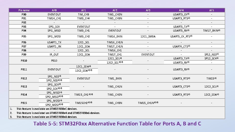
Pin name PB 0 PB 1 PB 2 PB 3 PB 4 AF 0 EVENTOUT TIM 14_CH 1 SPI 1_SCK SPI 1_MISO AF 1 TIM_CH 3 TIM 3_CH 4 EVENTOUT TIM 3_CH 1 AF 2 TIM 1_CH 2 N TIM 1_CH 3 N EVENTOUT AF 3 - AF 4 USART 3_CK(1) USART 3_RTS(1) USART 5_TX(1) USART 5_RX(1) AF 5 TIM 17_BKIN(1) PB 5 SPI 1_MOSI TIM 3_CH 2 TIM 16_BKIN 12 C 1_SMBA USART 5_CK_RTS(1) - PB 6 PB 7 PB 8 PB 9 USART 1_TX USART 1_RX IR_OUT 12 C 1_SCL 12 C 1_SDA EVENTOUT PB 10 - TIM 16_CH 1 N TIM 17_CH 1 N TIM 16_CH 1 TIM 17_CH 1 12 C 1_SCL(2) 12 C 2_SCL(1)(3) USART 4_CTS(1) USART 3_TX(1) USART 3_RX(1) SP 12_NSS(1) SP 12_SCK(1) - EVENTOUT 12 C 1_SDA(2) 12 C 2_SDA(1)(3) - - USART 3_RX(1) - TIM 1_BKIN - USART 3_RTS(1) TIM 15(1) TIM 1_CH 1 N - USART 3_CTS(1) 12 C 2_SCL(1) TIM 1_CH 2 N - USART 3_RTS(1) 12 C 2_SDA(1) TIM 1_CH 3 N TIM 15_CH 1 N(1)(3) - - PB 11 SPI 1_NSS(2) EVENTOUT SPI 2_NSS(1)(3) SPI 1_SCK(2) PB 13 SPI 2_SCK(1)(3) SPI 1_MISO(2) PB 14 TIM 15_CH 1(1)(3) SPI 2_MISO(1)(3) SPI 1_MOSI(2) PB 15 TIM 15 CH 2(1)(3) SPI 2_MOSI(1)(3) This feature is available on STM 32 F 030 x. C devices. This feature is availabel on STM 32 F 030 x 4 and STM 32 F 030 x 6 devices. This feature is available on STM 32 F 030 x 8 devices. PB 12 1. 2. 3. - Table 5 -5: STM 32 F 0 xx Alternative Function Table for Ports A, B and C

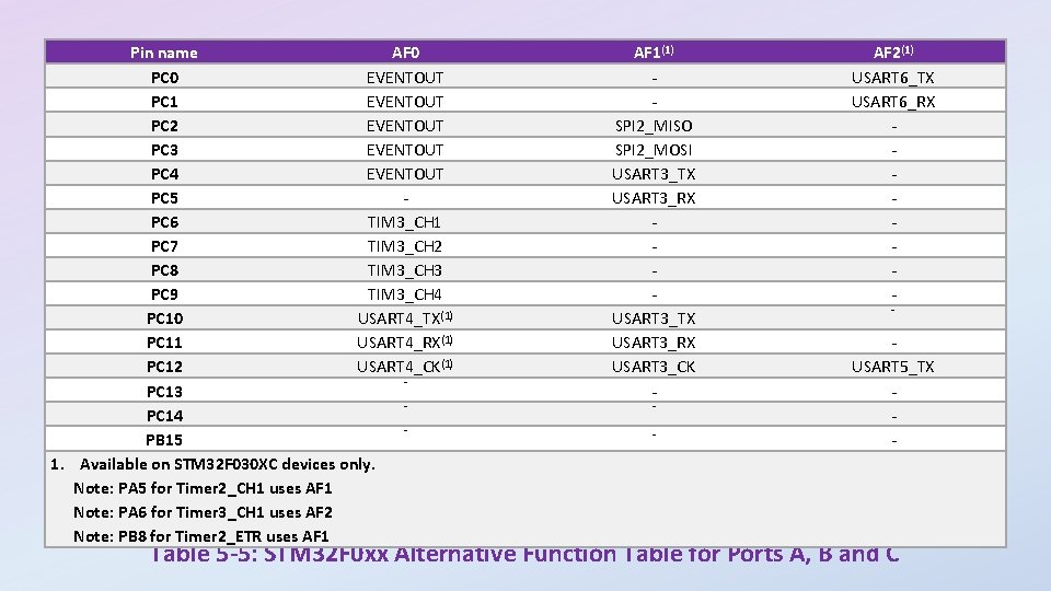
Pin name AF 0 PC 0 EVENTOUT PC 1 EVENTOUT PC 2 EVENTOUT PC 3 EVENTOUT PC 4 EVENTOUT PC 5 PC 6 TIM 3_CH 1 PC 7 TIM 3_CH 2 PC 8 TIM 3_CH 3 PC 9 TIM 3_CH 4 PC 10 USART 4_TX(1) PC 11 USART 4_RX(1) PC 12 USART 4_CK(1) PC 13 PC 14 PB 15 1. Available on STM 32 F 030 XC devices only. Note: PA 5 for Timer 2_CH 1 uses AF 1 Note: PA 6 for Timer 3_CH 1 uses AF 2 Note: PB 8 for Timer 2_ETR uses AF 1(1) SPI 2_MISO SPI 2_MOSI USART 3_TX USART 3_RX USART 3_CK - AF 2(1) USART 6_TX USART 6_RX - USART 5_TX - Table 5 -5: STM 32 F 0 xx Alternative Function Table for Ports A, B and C

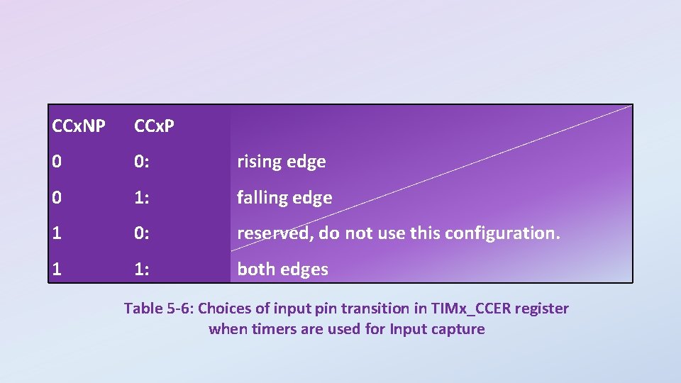
CCx. NP CCx. P 0 0: rising edge 0 1: falling edge 1 0: reserved, do not use this configuration. 1 1: both edges Table 5 -6: Choices of input pin transition in TIMx_CCER register when timers are used for Input capture

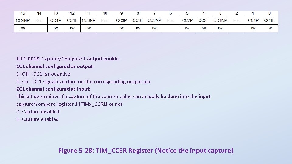
Bit 0 CC 1 E: Capture/Compare 1 output enable. CC 1 channel configured as output: 0: Off - OC 1 is not active 1: On - OC 1 signal is output on the corresponding output pin CC 1 channel configured as input: This bit determines if a capture of the counter value can actually be done into the input capture/compare register 1 (TIMx_CCR 1) or not. 0: Capture disabled 1: Capture enabled Figure 5 -28: TIM_CCER Register (Notice the input capture)

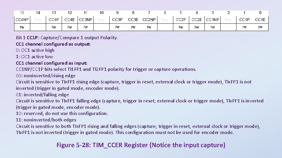
Bit 1 CC 1 P: Capture/Compare 1 output Polarity. CC 1 channel configured as output: 0: OC 1 active high 1: OC 1 active low CC 1 channel configured as input: CC 1 NP/CC 1 P bits select TI 1 FP 1 and TI 2 FP 1 polarity for trigger or capture operations. 00: noninverted/rising edge Circuit is sensitive to TIx. FP 1 rising edge (capture, trigger in reset, external clock or trigger mode), TIx. FP 1 is not inverted (trigger in gated mode, encoder mode). 01: inverted/falling edge Circuit is sensitive to TIx. FP 1 falling edge (capture, trigger in reset, external clock or trigger mode), TIx. FP 1 is inverted (trigger in gated mode, encoder mode). 10: reserved, do not use this configuration. 11: noninverted/both edges Circuit is sensitive to both TIx. FP 1 rising and falling edges (capture, trigger in reset, external clock or trigger mode), TIx. FP 1 is not inverted (trigger in gated mode). This configuration must not be used for encoder mode. Figure 5 -28: TIM_CCER Register (Notice the input capture)

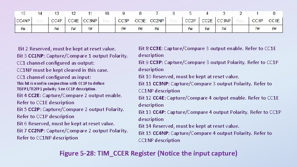
Bit 2 Reserved, must be kept at reset value. Bit 3 CC 1 NP: Capture/Compare 1 output Polarity. CC 1 channel configured as output: CC 1 NP must be kept cleared in this case. CC 1 channel configured as input: This bit is used in conjunction with CC 1 P to define TI 1 FP 1/TI 2 FP 1 polarity. See CC 1 P description. Bit 4 CC 2 E: Capture/Compare 2 output enable. Refer to CC 1 E description Bit 5 CC 2 P: Capture/Compare 2 output Polarity. Refer to CC 1 P description Bit 6 Reserved, must be kept at reset value. Bit 7 CC 2 NP: Capture/Compare 2 output Polarity. Refer to CC 1 NP description Bit 8 CC 3 E: Capture/Compare 3 output enable. Refer to CC 1 E description Bit 9 CC 3 P: Capture/Compare 3 output Polarity. Refer to CC 1 P description Bit 10 Reserved, must be kept at reset value. Bit 11 CC 3 NP: Capture/Compare 3 output Polarity. Refer to CC 1 NP description Bit 12 CC 4 E: Capture/Compare 4 output enable. Refer to CC 1 E description Bit 13 CC 4 P: Capture/Compare 4 output Polarity. Refer to CC 1 P description Bit 14 Reserved, must be kept at reset value. Bit 15 CC 4 NP: Capture/Compare 4 output Polarity. Refer to CC 1 NP description Figure 5 -28: TIM_CCER Register (Notice the input capture)

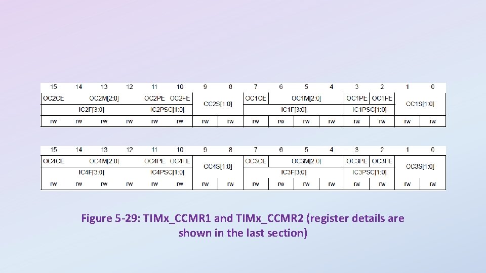
Figure 5 -29: TIMx_CCMR 1 and TIMx_CCMR 2 (register details are shown in the last section)

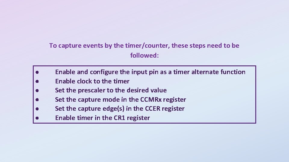
To capture events by the timer/counter, these steps need to be followed: · · · Enable and configure the input pin as a timer alternate function Enable clock to the timer Set the prescaler to the desired value Set the capture mode in the CCMRx register Set the capture edge(s) in the CCER register Enable timer in the CR 1 register

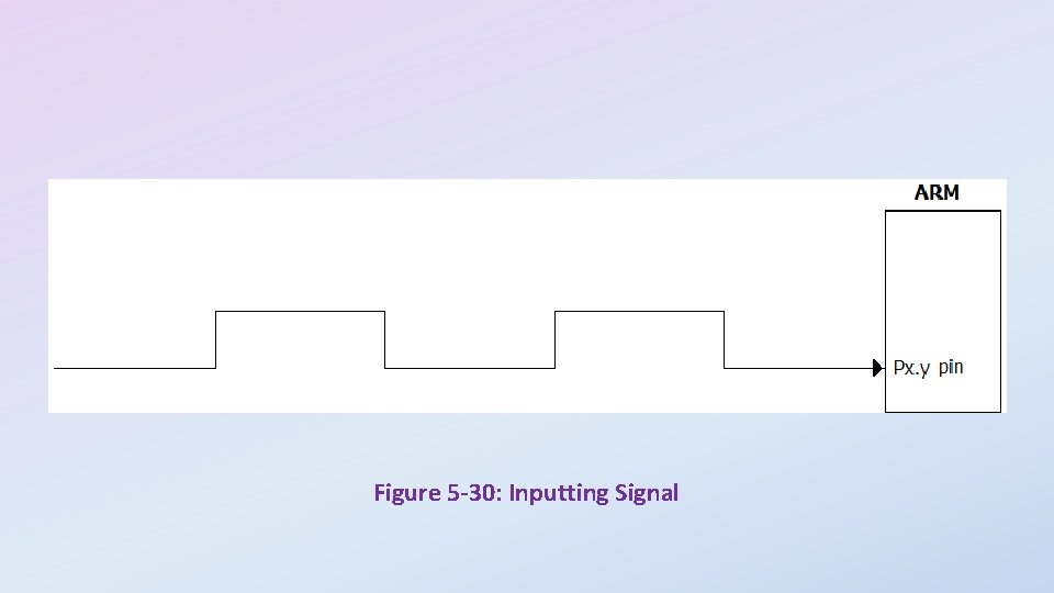
Figure 5 -30: Inputting Signal

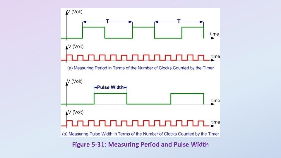
Figure 5 -31: Measuring Period and Pulse Width

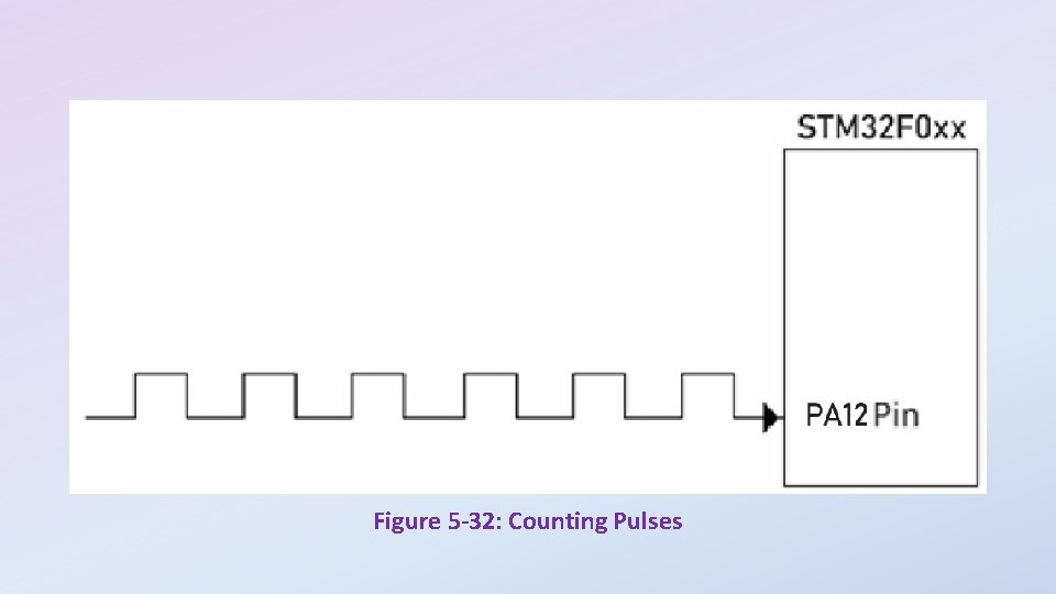
Figure 5 -32: Counting Pulses