Chapter 5 Sequential Systems Combinational logicthe output at
—the output at any instant of time depends only")
Chapter 5 Sequential Systems Combinational logic(组合逻辑)—the output at any instant of time depends only on what the inputs are at that time. Sequential system (时序系统)—the output will depend not only on the present input but also on the past history—what has happened earlier. 1
) A clock is just a signal")
Introduction n Clocked systems (referred to as synchronous(同步)) A clock is just a signal that alternates(over time) between 0 and 1 at a regular rate. clk 1 T clk 2 The period of the signal (T on the diagram) is the length of one cycle. The frequency is the inverse (1/T). Hz、KHz、MHz、GHz In most synchronous systems, it is the transition of the clock signal that causes changes to occur in sequential systems. 2
 Conceptual view of a sequential system clock n inputs Memory k")
Introduction (Con. ) Conceptual view of a sequential system clock n inputs Memory k outputs Combinational Logic m binary storage devices The combinational logic is a function of the system inputs and the contents of memory; the combinational logic outputs are the system outputs and signals to update the memory. 3
 new terminology to describe sequential systems n n State(状态): what is")
Introduction (Con. ) new terminology to describe sequential systems n n State(状态): what is stored in memory(binary devices). State table (状态表): shows for each input combination and each state, what the output is and what the next state is, that is, what is to be stored in memory after the next clock. n State diagram (or state graph) (状态图): a graphical representation of the state table. State Machines Finite State Machines(FSM) 4
 a sample state table to illustrate these definitions State table State")
Introduction (Con. ) a sample state table to illustrate these definitions State table State diagram 0/0 1/0 0/0 Input/Output column indicates the present state(现态); * columns indicate the next state(次态); The next state(次态)is a function of the present state(现态) and the input. Similarly, the output, , also depends on the present state and the input. each state a possible state transition 0/1 1/0 0/0 1/0 X/0 1/0 the input that causes that transition followed by the output that occurs This state diagram contains the identical information as the state table. 5
: a binary storage device, composed")
§ 5. 1 Latches and Flip Flops n Latch(闩锁、锁存器): a binary storage device, composed of two or more gates, with feedback(反馈). remark A NOR gate latch The normal storage state is both inputs 0(inactive). If S and R are 0, then state P is the opposite of Q. The latch can store either a 0(Q=0 and P=1)or a 1(Q=1 and P=0), thus, the P output is usually labeled. P=Q 0 0 P Q 0 1 reset 1 0 set 1 1 0 0 not allowed not the complement of each other (彼此) 6
 n n RS(Reset-Set)flip-flop: The Set (S)")
§ 5. 1 Latches and Flip Flops(Con. ) n n RS(Reset-Set)flip-flop: The Set (S) input causes a 1 to be stored in the flip flop at the next active clock edge; the Reset (R) input causes a 0 to be stored. Note: The S and R inputs are never made 1 at the same time. Q Q R S S 0 0 1 1 R 0 0 1 1 q 0 1 0 1 q* S 0 0 1 0 1 1 1 - - not allowed Behavioral table R 0 1 q* q 0 1 - 保持 复位 置位 不允许 置位 保持 10 00 01 0 RS 1 00 10 01 保持 复位 State diagram 置位 7
 S 0 0 1 1 R")
§ 5. 1 Latches and Flip Flops(Con. ) S 0 0 1 1 R 0 0 1 1 q 0 1 0 1 q* 0 1 0 0 1 1 - - We map q*. Notice that two of the squares are don’t cares, since we will never make both S and R equal to 1 at the same time. n q SR 00 01 11 10 0 x 1 1 1 0 x 1 RS-FF Behavioral table n Then we can write the equation: Note: RS=0 A timing example is shown in Figure 5. 16, on Page 334 8
 A gated latch When the Gate")
§ 5. 1 Latches and Flip Flops(Con. ) A gated latch When the Gate signal is inactive(=0, 无效), SG and RG are both 0, and the latch remains unchanged. Only when Gate goes to 1, can a 0 or 1 be stored in the latch. 9
 n Flip Flop(触发器): a clocked binary")
§ 5. 1 Latches and Flip Flops(Con. ) n Flip Flop(触发器): a clocked binary storage device; The state of the system changes on the transition of the clock. • That change takes place when the clock goes from 1 to 0; Note that the input must be available from that is referred to as trailing-edge triggered (下降沿触发 ). but is just before the clock begin to go down, • That change takes place the clock goes from 1; not when required after the output starts 0 to to change. that is referred to as leading-edge triggered (上升沿触发). Input must be stable Clock slanted to indicate that they do not change instantaneously Q Trailing-edge triggered flip flop timing diagram Delay 10
 of a flip flop can be described algebraically")
§ 5. 1 The next state(次态) of a flip flop can be described algebraically as a function of its inputs and present state. Flip-flops have one or two outputs. One output is the state In the of output the D flip flop, the equation is of the flip flop (thecase other is the complement of the state). We will introduce the D、JK、SR Latches and Flip Flops(Con. ) n q q D Trailing-edge triggered q and T flip flops. And we will use two forms of a truth table and a state diagram to describe the behavior of each type of flip flop. D Leading-edge triggered D flip-flop diagrams q D 0 0 1 1 q 0 1 q* 0 0 1 1 D 0 1 Truth table q* 0 1 1 0 0 D 1 0 State diagram 11 1
 The behavior of")
q § 5. 1 D q Latches and Flip Flops(Con. ) The behavior of a trailing-edge triggered D flip flop is illustrated in the timing diagram of figure 5. 9. Note that if the D input were to Clock go back and forth between clock transitions, the output would not be affected, since the value of D is only relevant near the time of a trailing edge. D q q D figure 5. 9 Clock A leading-edge triggered D flip flop is shown in figure 5. 10. D q figure 125. 10

 We connect the output of one")
§ 5. 1 Latches and Flip Flops(Con. ) We connect the output of one flip flop to the input of another, and clock them simultaneously, as shown in Figure 5. 11. x q D q r D r Clock x q r Clock Two flip flops That’s all. Timing for two flip flops Note: The output of flip flop r is a replica of that of q, delayed by one clock period. The name of the D flip flop comes from Delay. 14
 n The behavior of flip flops")
§ 5. 1 Latches and Flip Flops(Con. ) n The behavior of flip flops with static (asynchronous, 异步) clear(清零) and preset (预置) inputs. D PRE Clock Trailing-edge triggered CLR q q Clock CLR Active low Flip flop with clear and preset inputs PRE CLR D q q* 0 1 1 1 0 0 1 1 X X X 0 1 1 0 static immediate not allowed 0 0 clocked 1 (as before) 1 D D flip flop with clear and preset inputs q behavioral table Timing for flip flop with clear and preset 15
 n T 0 0 1 1")
§ 5. 1 Latches and Flip Flops(Con. ) n T 0 0 1 1 q 0 1 T Clock T(Toggle) flip-flop: only one input, T, such that if T=1, the flip flop changes state (that is, is toggled), and if T=0, the state remains the same. q* 0 1 1 0 q* q 保持 q 翻转 0 0 T 0 1 0 0 1 1 1 0 q 1 T 0 1 T 1 0 1 State diagram q The behavioral equation is: q A timing example is shown in Figure 5. 18, on Page 335 16

q JK § 5. 1 0 0 0 1 00 11 10 1 1 Latches and Flip Flops(Con. ) 1 0 0 1 n J 0 0 1 1 01 K 0 0 1 1 J q K q JK flip-flop: itq*is a combination of the RS and T. q 0 1 0 1 q* 0 1 0 0 1 1 1 0 J 0 0 1 1 K 0 1 q* q 0 1 q 10 11 保持 复位 置位 翻转 00 01 0 JK 1 00 10 01 11 State diagram JK-FF Behavioral table From the first truth table, we can map it and derive the equation for q*: A timing example is shown in Figure 5. 20, on Page 336 17
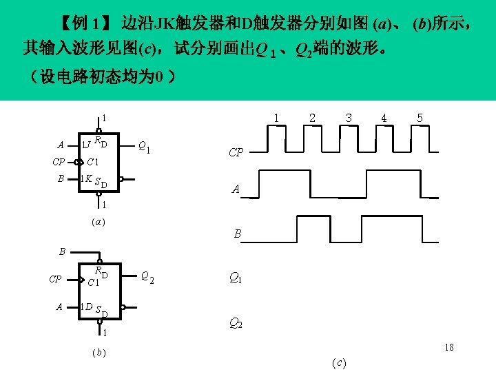

第 5章 触发器 1 A 1 J RD CP C 1 B 1 K S D 分析: Q 1 1 1 3 4 5 A B A 2 ) CP (a) CP (当B=0时, RD C 1 Q 2 B 1 D S D 1 Q 1 (b) Q 2 设电路初态均为 0 ( c) 19
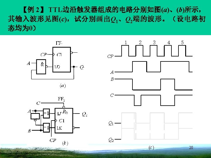

FF 1 CP A & 1 C 1 1 D Q 1 A 1 B 1 J RD C 1 1 K =1 CP (b ) 4 5 CP C FF 2 =1 3 A B (a ) C 2 Q 1 Q 2 (c ) 21

 n n Some of the commercially")
§ 5. 1 Latches and Flip Flops(Con. ) n n Some of the commercially available flip flop packages D and JK flip flops are the most common. 7473: a dual JK flip flop package 7474: a dual D flip flop package 74174: a hex(six) D flip flop package 74175: a quad(four) D flip flop package 24

§ 5. 2 Analysis of Sequential Systems Do some review. Some Edge-Triggered Flip-Flops FFs Symbols: RSFF DFF JKFF TFF Characteristic Equations: RSFF: Positive-edge-triggered FF DFF: JKFF: TFF: Negative-edge-triggered FF 25

§ 5. 2 Analysis of Sequential Systems Objectives n This section introduces synchronous sequential systems with the following goals: u Definition of synchronous sequential systems u Introduce two versions models of sequential circuits: Mealy and Moore models u Demonstrate by example how to analyze synchronous sequential circuits n Reading Assignment u Mealy and Moore Models: P 337 u Analysis of sequential circuits: P 343 26

§ 5. 2 Analysis of Sequential Systems n Definition: A sequential circuit is said to be a synchronous sequential system if it satisfies the following conditions: Ø All flip-flops have the same type of dynamic clock Ø All clock inputs of all the flip-flops are driven by the same clock signal. 27

§ 5. 2 Analysis of Sequential Systems clock Memory Combinational Logic Output Equation Input Equation State Equation 28

§ 5. 2 Analysis of Sequential Systems Two different type sequential models clock Memory Combinational Logic Y=G(X, Q) Q*=H(Y, Q) Z=F(X, Q) A sequential system whose output depends on both state and input is called a Mealy-type output. 29

§ 5. 2 Analysis of Sequential Systems Two different type sequential models clock Memory Combinational Logic Y=G(X, Q) Q*=H(Y, Q) Z=F(Q) A sequential system whose output depends on the 30 state alone is called a Moore-type output.
 n n n The Classification")
§ 5. 2 Analysis of Sequential Systems (Con. ) n n n The Classification of Sequential Systems On the basis of the characteristic of State change: Synchronous Sequential systems Asynchronous Sequential Systems On the basis of the characteristic of Output signals(P 337): Mealy model: the output depends on the current input as well as the contents of memory. Z=F(X, Q) Moore model: the output depends only on the present state of the system. Z=F(Q) 31
 n n n Functional description")
§ 5. 2 Analysis of Sequential Systems (Con. ) n n n Functional description of Sequential Systems Logic Equation Z=F(X, Q) Q*=H(Y, Q) Y=G(X, Q) State Transition Table (that is: State Table) Mealy model: Next states/Outputs Moore model: Next states and Outputs are listed respectively State diagram Timing graph 32
 n State Transition Table (that")
§ 5. 2 Analysis of Sequential Systems (Con. ) n State Transition Table (that is: State Table) 00 01 11 10 00 00/0 01/1 00/0 10/0 01 01/1 00/0 11/1 10 10/1 11/1 0 1 00 01 11 0 11/1 01 10 00/0 11/1 11 00 10 1 00/0 10/1 10 11 01 0 Mealy model Moore model 33
 n State diagram 01/0 00/0")
§ 5. 2 Analysis of Sequential Systems (Con. ) n State diagram 01/0 00/0 11/0 00 10/1 11/0 10 11/0 00/0 11/0 01/1 00/1 01/1 00 01 11 10 00 00/0 01/1 00/0 10/0 01 01/1 00/0 11/1 11 00/0 11/1 10 10/1 11/1 00/0 10/1 01 XX/Z 10/1 11 00/1 10/1 Mealy model Q 1 Q 0 01/1 10/1 Moore model 34
 n State diagram 0 1")
§ 5. 2 Analysis of Sequential Systems (Con. ) n State diagram 0 1 00 01 11 0 01 10 00 0 11 00 10 11 01 0 Mealy model Moore model 35
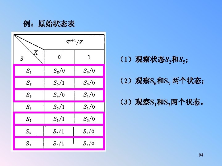
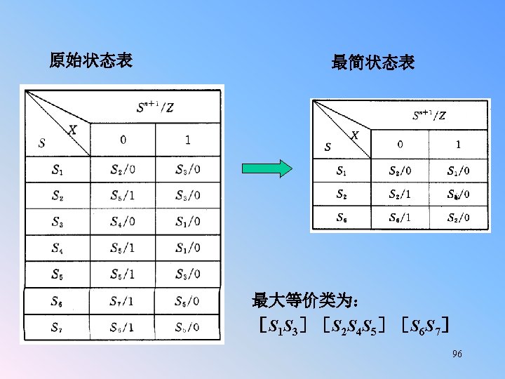
 table 【状态(转移)表】 Ø")
Sequential systems can be represented in many forms. Ø State (transition) table 【状态(转移)表】 Ø State diagram 【状态图】 Ø State equations 【状态方程】 Ø Flip-flop input (excitation) funcations 【激励方程】 Circuit output functions 【输出方程】 Ø Timing diagram 【时序图】 Ø Circuit diagram 【电路图】 These equivalent forms show the inputs, outputs, and flipflop state changes for sequential circuits. 36
 n The Steps of analysis")
§ 5. 2 Analysis of Sequential Systems (Con. ) n The Steps of analysis Logic Circuit Input equation Output equation State Diagram Function Timing 37

§ 5. 2 Analysis of Sequential Systems Analysis Example 5. 2. 1 A simple synchronous sequential circuit with two negative-edge-triggered JK flip-flops. Please analyze its behavior. n At the trailing edge of the clock signal (CP), each JKFF samples its JK inputs and transfers these values to its Q output. Therefore, to determine the next value of Q (Q*), we must first determine the current value of J and K. 38

§ 5. 2 Analysis of Sequential Systems Analysis Example 5. 2. 1 X Q 1 Q 0 1. Derive the excitation and output equations J 0=K 0=1 J 1=K 1= Mealy-type output 39

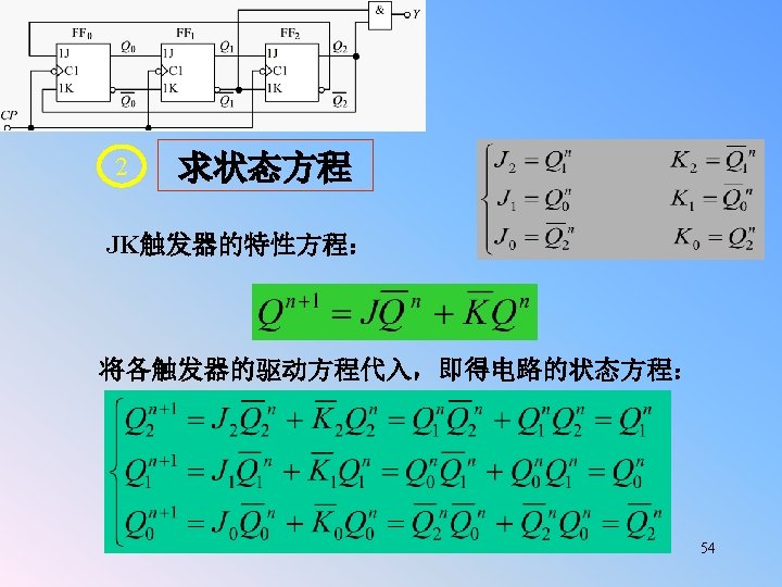
§ 5. 2 Analysis of Sequential Systems Analysis Example 5. 2. 1 2. Derive the state equations from the excitation equations J 0=K 0=1 J 1=K 1= u Use the characteristic equation for JK flip-flops: u The resulting state equations are: 40
 41")
3. State table and state diagram (列状态表,画状态图) 41

state diagram 0/0 00 0/0 1/1 11 01 1/0 10 0/0 X/ Z Q 1 Q 0 0/0 43
 1 2 3 4 5 6")
4. Timing graph (Initial states are 0. ) 1 2 3 4 5 6 7 8 9 CP X Q 0 Q 1 Z 44

5. Logical Function From the state diagram, we can see: If X=0, its state 00→ 01→ 10→ 11→ 00→… If X=1, its state 00→ 11→ 10→ 01→ 00→… This is a synchronous up/down counter and its module is 4. Where, X is control signal of up/down. Z is carry/borrow signal. 45 That’s all for today!

§ 5. 2 Analysis of Sequential Systems In summary The detailed steps for analyzing a synchronous systems are as follows: u Determine the excitation equations (激励方程) for the flip -flop control inputs. u Substitute the excitation equations into the flip-flop characteristic equations to obtain state equation (状态方程). u Use the state equations to construct a state table (状态表). u Determine the output equations (输出方程). u Draw a state transition diagram (状态图) corresponding to the state/output table. u Obtain the behavior (逻辑功能) of the circuit. 46
 n Example 5. 2. 1")
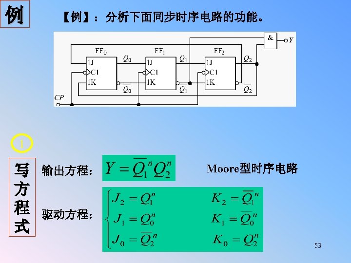
§ 5. 2 Analysis of Sequential Systems (Con. ) n Example 5. 2. 1 Explanation: 2. State equation 1. Input and Output equations 47

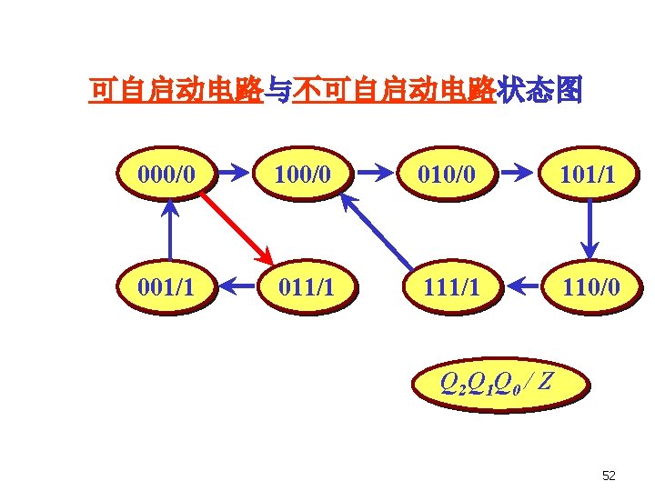
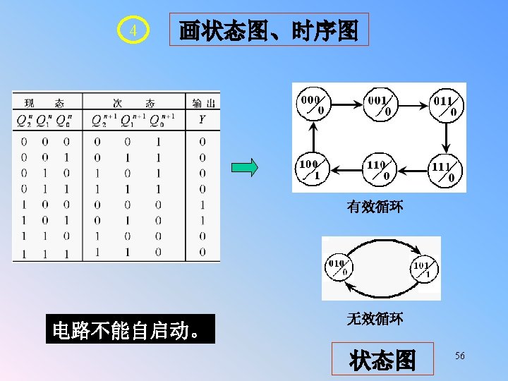
2. State equation 3. State table and state diagram This sequential circuit is Moore model. 000 001 010 101 100 111 110 Q 2 Q 1 Q 0 011 有效状态、无效状态、自启动 48
 1 2 3 4 5 6 CP Q 0 0")
4. Timing graph (时序波形) 1 2 3 4 5 6 CP Q 0 0 Q 1 0 Q 2 0 49
 Pulse distributor 50")
5. Logical Function (逻辑功能) Pulse distributor 50


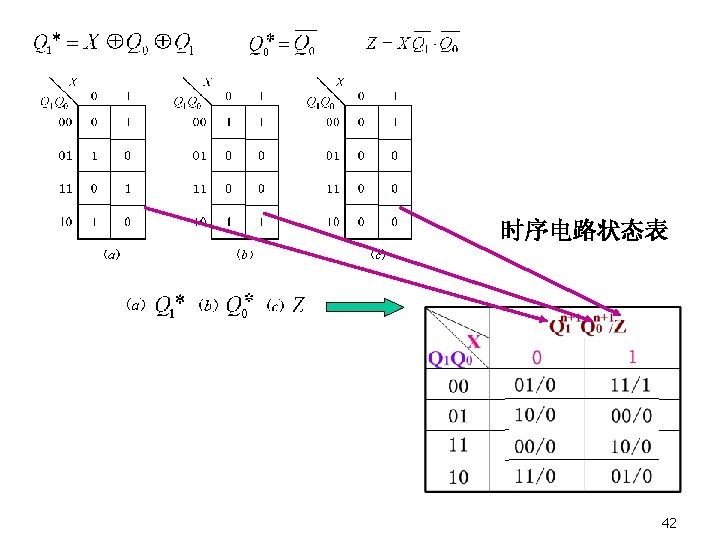
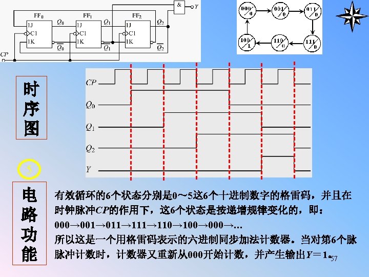
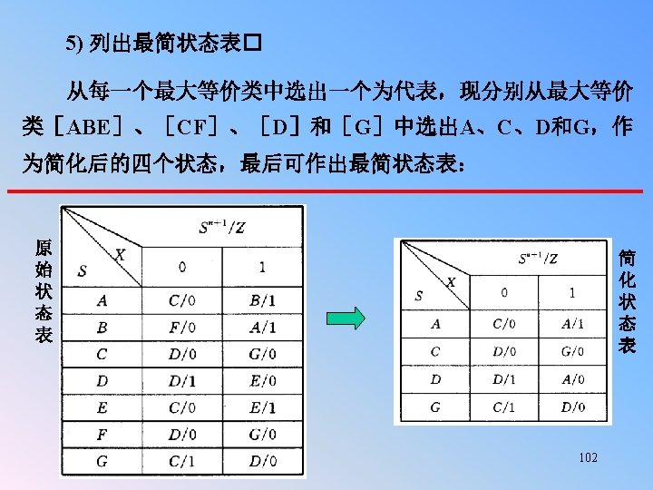
3 列状态表 0 0 1 1 0 0 1 1 0 1 0 1 1 1 0 0 0 0 1 1 0 055
 (b) (c) 58")
Examples: (a) (b) (c) 58
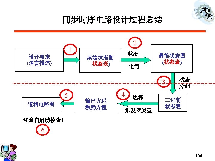
 1 Design aim")
§ 5. 3 The Design Process for Synchronous Sequential Systems(P 337) 1 Design aim (Word description) 2 Original State diagram (state table) State reduce Reduced State diagram (state table) 3 5 Logic Circuit To check whether it can turn on by itself? Input equation Output equation Select the type of Flip Flops State assign Binary state table 4 6 59
: This table")
§ 5. 4 Flip-Flop Design Techniques The flip-flop design table (input equation): This table allows us to determine the inputs of the flip-flop, which can be most readily obtained from the state diagram. n 1 0 state diagram 0 1 D 1 0 1 0 Flip-flop design table 0 0 1 1 q* 0 1 1 0 0 1 D q 0 1 0 0 1 1 Excitation table q* 0 1 T 0 1 1 1 0 q JK 0 J 0 1 X X K X X 1 0 q 0 0 1 1 q* 0 1 T 0 1 1 0 60
 n Example 5. 4. 1 (P")
§ 5. 4 Flip-Flop Design Techniques (Cont. ) n Example 5. 4. 1 (P 352 Table 5. 15) State table: * x 0 0 1 1 Input (excitation) table: 0 0 1 1 0 1 0 1 0 0 0 1 1 1 * 0 0 1 0 1 1 Truth table to develop flip flop inputs * x 0 0 1 1 0 1 0 1 0 0 0 1 1 1 * 0 0 1 0 1 1 0 0 0 1 1 1 0 0 1 0 1 1 0 0 X X 0 1 X X 1 1 X X 0 0 0 X 1 X 1 X 0 0 0 1 1 1 1 0 Map the K-Map of the D and J、K and T , then we can obtain the Logic of flip-flop inputs 61
 n n FF")
Implementation using JK-FF: § 5. 4 Flip-Flop Design Techniques (Cont. ) n n FF 1 Example 5. 4. 1 FF 2 1) (Method For the JK flip flop, the resulting maps are shown as below. (P 353 Map 5. 5) x 0 1 00 X X 00 1 01 X X 01 00 01 x 11 X X 11 10 X X 10 1 10 0 1 x 0 1 1 00 X X 01 1 1 X X 11 1 1 10 X X The JK-FF input equations are 62
 FF 1 Example")
Implementation using JK-FF: § 5. 4 Flip-Flop Design Techniques (Cont. ) FF 1 Example 5. 4. 1 n FF 2 2) (Method The quick method for JK flip flop design (it does not apply to the other types of flip flop) takes advantage of a property of JK flip flops. n * x 0 0 1 1 0 1 0 1 0 0 0 1 1 1 x * 0 0 1 0 1 00 x 00 0 1 1 01 11 1 10 1 State Equation of JK flip flop is Compared 63
 n * x 0 0 1")
§ 5. 4 Flip-Flop Design Techniques (Cont. ) n * x 0 0 1 1 0 1 0 1 0 0 0 1 1 1 Example 5. 4. 1 * 0 0 1 0 1 1 How to do with D flip-flop? State Equation of DFF is 64
 n n In this")
§ 5. 5 The Design of Synchronous Counters (P 365) n n In this section, we will look at the design of a type of synchronous sequential system referred to as a counter( 计数器). 【term: Module(模)】 Most counters are devices with no data input, that go through a fixed sequence of states on successive clocks. The output is often just the state of the system, that is the contents of all of the flip flops. clock 65
 n n Classification of")
§ 5. 5 The Design of Synchronous Counters (Cont. ) n n Classification of the Counters: On the basis of control mode of the clock: Synchronous Counters & Asynchronous Counters On the basis of the up or down of the sequence: up counters & down counters & up/down counters On the basis of the module of the counters: binary counters 、decimal counters & any system counters Name Binary counter Decimal counter Any system counter Module code mode Binary BCD-code Any mode Can turn on by itself ? no redundant states, can 6 redundant states need check redundant states 66
 n Example: An up/down")
§ 5. 5 The Design of Synchronous Counters (Cont. ) n Example: An up/down binary counter, where x is control input, such that the counter counts up when x=0 and down when x=1. (Using JKFF. ) The state table is : How to do with JK flip-flop? * * x 0 0 0 0 1 1 1 1 0 0 1 1 0 1 0 1 0 0 0 1 1 0 1 0 0 1 1 0 0 1 1 0 0 1 * 1 0 1 0 67

n Example: An up/down binary counter, where x is control input, such that the counter counts up when x=0 and down when x=1. (Using JKFF. ) * * x 0 0 0 0 1 1 1 1 0 0 1 1 0 1 0 1 0 0 0 1 1 0 1 0 0 1 1 0 0 1 1 0 0 1 * 1 0 1 0 JK-FF: JKFF_A JKFF_B JKFF_C 68

n Example: An up/down binary counter, where x is control input, such that the counter counts up when x=0 and down when x=1. (Using JKFF. ) JK-FF: * * x 0 0 0 0 1 1 1 1 0 0 1 1 0 1 0 1 0 0 0 1 1 0 1 0 0 1 1 0 0 1 1 0 0 1 * 1 0 1 0 x. C BA 00 00 01 1 11 10 01 11 10 * 69

n Example: An up/down binary counter, where x is control input, such that the counter counts up when x=0 and down when x=1. (Using JKFF. ) * * x 0 0 0 0 1 1 1 1 0 0 1 1 0 1 0 1 0 0 0 1 1 0 1 0 0 1 1 0 0 1 1 0 0 1 * 1 0 1 0 x. C BA 00 01 11 10 00 1 1 1 01 11 1 10 1 1 01 1 1 11 10 1 1 * x. C 00 01 10 11 BA BA 00 01 11 10 00 00 1 1 1 1 01 1 1 * 1 11 10 1 1 1 * From these maps, we can see that: 70 1

n Example: An up/down binary counter, where x is control input, such that the counter counts up when x=0 and down when x=1. (Using JKFF. ) * * x 0 0 0 0 1 1 1 1 0 0 1 1 0 1 0 1 0 0 0 1 1 0 1 0 0 1 1 0 0 1 1 0 0 1 * 1 0 1 0 How to do with D flip-flop? State Equation of DFF is 71
 Example 5. 5. 1:")
§ 5. 5 The Design of Synchronous Counters (Cont. ) Example 5. 5. 1: Design a synchronous counter using JK flip flop, n whose module is 5. State transition is shown as below 000 001 011 101 110 Explanation: 1. List the state table According to the subject, there are 3 state-variables, which are refered to as 、. Then binary state table as follows. 0 0 0 1 1 0 1 0 1 0 0 X 1 0 X 0 1 1 1 X X 0 1 X X 1 0 0 0 X X 1 0 00 X 00 01 1 01 X 11 11 1 10 X 10 1 X 1 、 0 1 X X 00 1 1 01 1 X 11 1 10 X X 72

0 1 0 00 X 00 01 1 01 X 11 11 1 10 X 1 1 1 X X 00 1 1 01 1 X 11 1 10 X X 10 0 X 2. Input equations and Output equations table 1: redundant state transition From the K-maps shown as above: The state ‘ 100 ’ 0 cycle 1 0 !1 can’t go into the main 1 1 3. Check whether it can go into the main cycle from any initial state. Process: According to the state equations, the next states of the redundant states are shown as table 1 and the whole state diagram is shown as fig. 1: 0 1 111 0 0 0 100 000 Q 2 Q 1 Q 0 110 001 010 101 011 Figure 1: state diagram 73

111 100 000 Q 2 Q 1 Q 0 110 001 010 101 011 The state ‘ 100’ can’t go into the main cycle ! How to do next ? Figure 1: state diagram Method 1: turn the incompletely specified logic into the completely specified logic, then the state table of the completely spcified sequential logic is shown as below. 0 0 1 1 0 1 0 1 0 0 0 X 1 0 X 0 0 X 1 0 X 0 1 1 0 X 0 74

0 111 Q 2 Q 1 Q 0 110 010 100 001 101 011 1 0 00 X 00 01 1 01 X 11 11 1 10 X 10 1 1 0 1 X X 00 1 1 01 1 X 11 1 10 X X X Method 2: Changing the original way of the K-map cycling. From the above state diagram, we can see that only the state ‘ 100’ can’t go into the main cycle. Then we can only change the K-map of. 0 1 00 1 X 01 1 10 X X redundant state transition table 0 1 1 1 0 0 0 111 000 Q 2 Q 1 Q 0 010 110 001 100 101 011 state diagram 75
 n Example : Design")
§ 5. 5 The Design of Synchronous Counters (Cont. ) n Example : Design a synchronous up counter using D flip flop, whose module is 7. 76 That’s all for today!

§ 5. 7 Derivation of State Tables and State Diagrams n n n In this section, we will start with verbal description of sequential systems and develop state diagrams or tables. Example(CE 6): A system with one input x and one output z such that z=1 at a clock time iff x is currently 1 and was also 1 at the previous two clock times. Another way of wording this same problem is: CE 6#: A Mealy system with one input x and one output z such that z=1 iff x has been 1 for three consecutive clock times. 77
 Derivation of State Tables and State Diagrams n A")
§ 5. 7 (Cont. ) Derivation of State Tables and State Diagrams n A simple input/output trace for such a system is shown in Timing Trace 5. 3 (as below): x 0 1 1 1 1 0 1 z 0 0 0 1 1 1 0 0 0 1 0 0 We can see from the trace that the intent of the problem statement is “three or more” consecutive 1’s or “at least three” consencutive 1’s. The question is: when the input is 1, what do we need to know about previous inputs to determine whether the output should be 1 or not, and to update memory? (Of course, we know that if the input is 0, the output is 0. ) 78
 Derivation of State Tables and State Diagrams n The")
§ 5. 7 (Cont. ) Derivation of State Tables and State Diagrams n The first step in this problem, as it is in many word problems, is to determine what needs to be stored in memory. For this problem, there are two approaches: First, we could save the previous two inputs. Knowing them and the present input, we could determine the output. A state table for this approach is shown as below, where the first bit (q 1 ) is the older input and the second (q 2 ) the more recent one. q* q* z 1 2 q q 1 0 0 1 1 2 0 1 x=0 0 0 1 0 x=1 0 1 1 1 x=0 0 0 x=1 0 0 0 1 79
 Derivation of State Tables and State Diagrams For the")
§ 5. 7 (Cont. ) Derivation of State Tables and State Diagrams For the second approach, we store in memory the number of consecutive 1’s, as follows: A none, that is the last input was 0 B one 1 C two or more 1’s That is, if the present input is a 0, the next state is A; otherwise, we move from A to B and from B to C. The state diagram is shown in Figure 5. 35 (as following). 80
 Derivation of State Tables and State Diagrams The state")
§ 5. 7 (Cont. ) Derivation of State Tables and State Diagrams The state table: The state diagram: 0/0 A 1/0 0/0 B one 1 1/0 no 1’s 0/0 C Two or more 1’s q 1 q 2 q*1 q*2 x=0 x=1 z x=0 x=1 A A B 0 0 B A C 0 0 C A C 0 1 1/1 ◆Consider the difference if the problem changes to producing a 1 if the input has been 1 for 25 consecutive clock times. Now the first approach requires us to store the last 24 inputs (in 24 flip flops) and a state table of 224 rows. The second approach requires 25 states (indicating 0 consecutive 1’s, 1 consecutive 1, … , 24 or more consecutive 1’s). These 25 states can be coded with 5 flip flops. 81
 q* q* z 1 2 q q 1 2")
§ 5. 7 (Cont. ) q* q* z 1 2 q q 1 2 x=0 x=1 0 0 0 1 1 1 0 0 0 1 1 is 0 to reduce 1 1 process the state Derivation of State Tables and State Diagrams n The next step in the design table, if possible, to one with fewer state (Chapter 7). For the first design, the state assignment has already been made. We labeled the flip flops q 1 and q 2. Following map shows the next state and we solve for D flip flops and JK flip flops. 0 1 00 01 1 1 01 11 10 10 * * 1 1 z 82
 Derivation of State Tables and State Diagrams For the")
§ 5. 7 (Cont. ) Derivation of State Tables and State Diagrams For the three-state system of the second approach, there are three basically different state assignments, as shown in table 5. 19. A 1/0 0/0 B one 1 1/0 no 1’s q q 1 q 2 0/0 Two or more 1’s A B C 0 0 1 A B C 0 1 0 C 1/1 (a) 0 1 0 0 1 1 (b) 0 1 1 (c) Thus, three State Tables are: 83

q 1 q 2 q q 1 q 2 A B C 0 0 1 0 (a) q q 1 q 2 A B C 0 0 1 (b) 0 1 1 q*2 x=0 x=1 z x=0 x=1 A A B 0 0 B A C 0 0 C A C 0 1 q 2 q*1 q*2 x=0 x=1 0 0 0 1 z x=0 x=1 0 0 0 0 1 q 1 q 2 q*1 q*2 x=0 x=1 0 0 0 1 1 1 z x=0 x=1 0 0 0 0 1 1 0 1 84

q 1 q 2 q q 1 q 2 A B C 0 1 0 (c) 0 1 1 q*2 x=0 x=1 z x=0 x=1 A A B 0 0 B A C 0 0 C A C 0 1 q 2 q*1 q*2 x=0 x=1 0 0 1 1 0 1 z x=0 x=1 1 1 0 0 0 0 0 1 0 1 85
 : Design a Mealy system with one input")
n Example 5. 11 (P 382) : Design a Mealy system with one input x and one output z such that z=1 iff x has been 1 for exactly three consecutive clock times. A sample input/output trace for this system is: x 0 1 1 1 1 0 1 z 0 0 0 0 1 0 0 0 We cannot tell whethere should be a 1 output when the third consecutive 1 input occurs. From the trace, it is not until the next input arrives that we know that there have been exactly three 1’s in a row. So we now need five states. A none, that is the last input was 0 B one 1 in a row C two 1’s in a row D three 1’s in a row E too many (more than 3) 1’s in a row 86

A B C D E none, that is the last input was 0 one 1 in a row two 1’s in a row three 1’s in a row too many (more than 3) 1’s in a row The state diagram: 0/0 1/0 one 1 A 0/0 B 1/0 C two 1’s more than three 1’s E 0/0 0/1 1/0 1/0 D three 1’s The implementation of this system requires three flip flops. 87
 : Design a Mealy system whose output is")
n Example 5. 12 (P 383) : Design a Mealy system whose output is 1 iff the input has been 1 for three consecutive clocks, but inputs are nonoverlapping. (That means that a 1 input can only be used toward one 1 output. ) A sample input/output trace for this system is: x 0 1 1 1 1 0 1 z 0 0 0 1 0 0 We need three states: A B C The state diagram: none or three 1’s one 1 two 1’s 0/0 A no 1’s 1/0 0/0 one 1 B 1/0 1/1 0/0 C two 1’s 88
 : Design a Mealy system where the inputs")
n Example 5. 13 (P 384) : Design a Mealy system where the inputs are considered in blocks of three. The output is 1 iff the input is 1 for all three inputs in a block; obviously, that 1 output cannot occur until the third input is received. A sample input/output trace for this system is: x 0 1 1 1 0 1 z 0 0 0 1 1 1 0 0 0 1 From the problem: the initial state, A 1/1 0/0 D A state table with seven states: A X/0 1/0 B X/0 1/0 0/0 E 0 1 0 0/0 X/0 C 1/0 0/0 F G q x=0 A B C D E F G C E G A A q* x=1 x=0 B D F A A 0 0 0 0 F and G are two extra states. z x=1 0 0 0 89

Replaced F and G using E, then the state table with five states: Example 5. 13 (Con. ): q x=0 A B C D E F G C E G A A q x=0 A B C D E C E E A A q* q* x=1 x=0 B D F A A 0 0 0 0 x=1 x=0 B D E A A 0 0 0 z x=1 0 0 0 1/1 0/0 D A X/0 1/0 B 0/0 X/0 1/0 D 1/0 0/0 F E 1/1 0/0 C G A B 1/0 0/0 X/0 0/0 C X/0 E 90


 : Design a Moore system with an output")
n Example 5. 15 (P 385) : Design a Moore system with an output of 1 iff the input has been 1 for at least three consecutive clocks. In a Moore system, the output changes after the clock on which the third input is 1. Furthermore, the output remains valid until the next clock (in contrast to a Mealy system where it is only valid at the clock time). Z=F(Q) A sample input/output trace for such a system is: x 0 1 1 1 1 0 1 z 0 0 1 1 1 0 0 0 1 0 0 x Q z 0 clock trigger no 1’s A/0 1 0 one 1 B/0 1 0 C/0 two 1’s 0 1 three or more 1’s D/1 1 That’s all for 103 today!

n Example : Design a Sequence Detector which can detect the sequence of “ 111”. 105
 4. 5. 7. 8. (a, b) n 9. (b)")
Ch 5 Ex. (P 424) 4. 5. 7. 8. (a, b) n 9. (b) n 12. (i, iv) a. b. 16. n 106
- Slides: 106