Chapter 5 Resistor Transistor Logic RTL Digital Electronics
- Slides: 35

Chapter 5 Resistor Transistor Logic - RTL Digital Electronics ELE 450 A First 2015/2016 Dr. Idrees Al-Kofahi 1

Resistor Transistor Logic • • The resistor Transistor Logic family is a family of logic gates that are made exclusively of resistors and transistors. The basic gate in every family is the inverter. The inverter is used to study the basic behavior of the logic gates. More complex gates are analyzed only to point out differences in behavior. The basic RTL inverter is the same as the BJT inverter we mentioned earlier. Digital Electronics ELE 450 A First 2015/2016 Dr. Idrees Al-Kofahi 2

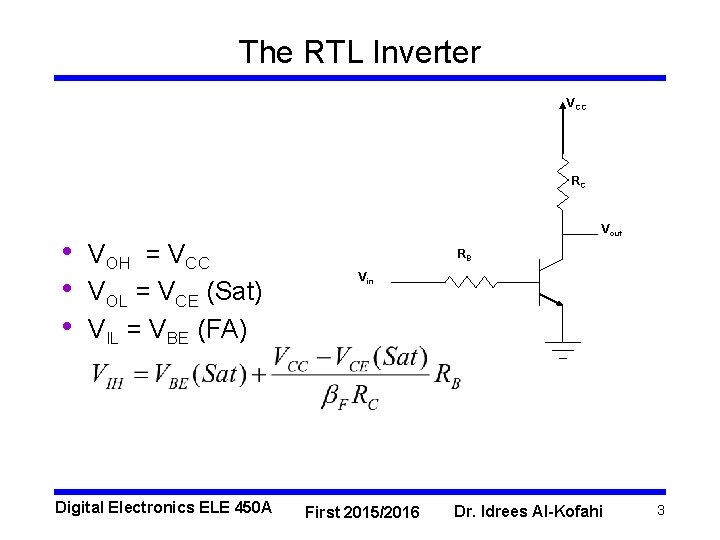
The RTL Inverter VCC RC • • • Vout VOH = VCC VOL = VCE (Sat) VIL = VBE (FA) Digital Electronics ELE 450 A RB Vin First 2015/2016 Dr. Idrees Al-Kofahi 3

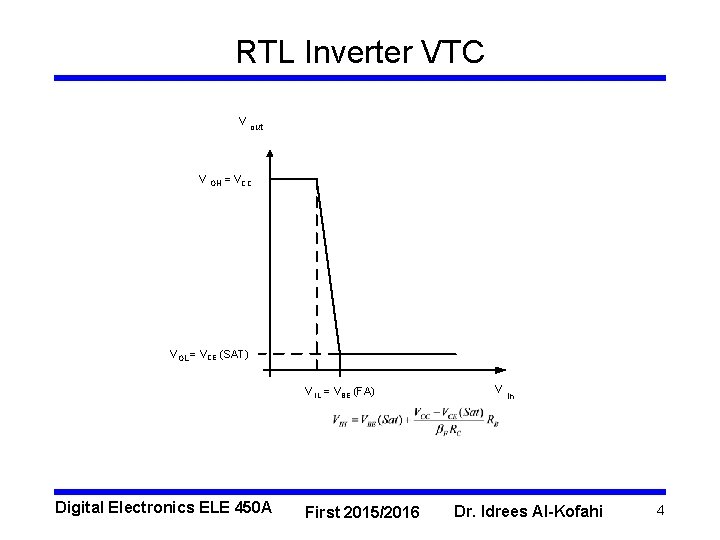
RTL Inverter VTC V out V OH = VCC VOL = VCE (SAT) V IL = VBE (FA) Digital Electronics ELE 450 A First 2015/2016 V in Dr. Idrees Al-Kofahi 4

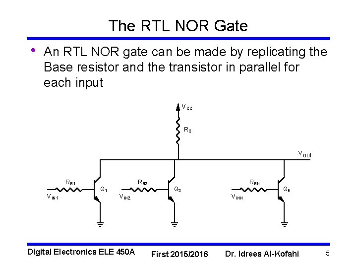
The RTL NOR Gate • An RTL NOR gate can be made by replicating the Base resistor and the transistor in parallel for each input V CC RC V out RB 1 V IN 1 RB 2 Q 1 Q 2 V IN 2 Digital Electronics ELE 450 A RBN QN V INN First 2015/2016 Dr. Idrees Al-Kofahi 5

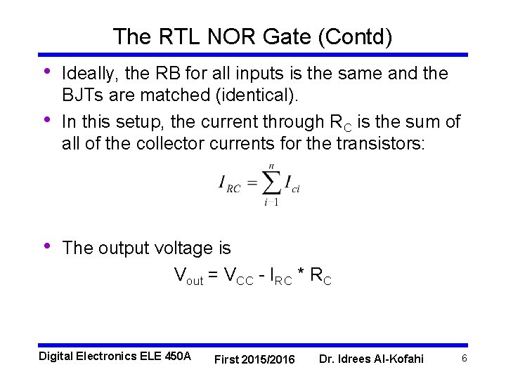
The RTL NOR Gate (Contd) • • • Ideally, the RB for all inputs is the same and the BJTs are matched (identical). In this setup, the current through RC is the sum of all of the collector currents for the transistors: The output voltage is Vout = VCC - IRC * RC Digital Electronics ELE 450 A First 2015/2016 Dr. Idrees Al-Kofahi 6

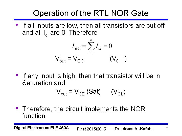
Operation of the RTL NOR Gate • If all inputs are low, then all transistors are cut off and all Ici are 0. Therefore: Vout = VCC (VOH ) • If any input is high, then that transistor will be in Saturation and Vout = VCE (Sat) (VOL) • Therefore, the circuit implements the NOR function. Digital Electronics ELE 450 A First 2015/2016 Dr. Idrees Al-Kofahi 7

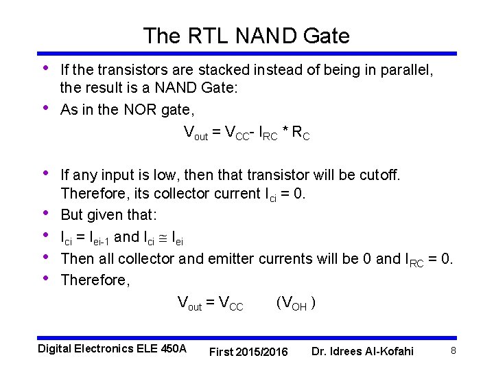
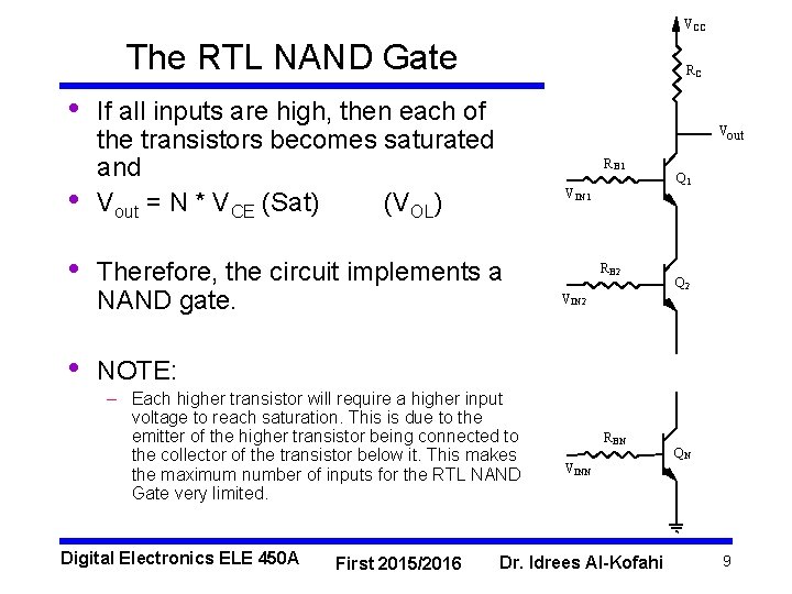
The RTL NAND Gate • • If the transistors are stacked instead of being in parallel, the result is a NAND Gate: As in the NOR gate, Vout = VCC- IRC * RC If any input is low, then that transistor will be cutoff. Therefore, its collector current Ici = 0. But given that: Ici = Iei-1 and Ici Iei Then all collector and emitter currents will be 0 and IRC = 0. Therefore, Vout = VCC (VOH ) Digital Electronics ELE 450 A First 2015/2016 Dr. Idrees Al-Kofahi 8

VCC The RTL NAND Gate • • RC If all inputs are high, then each of the transistors becomes saturated and Vout = N * VCE (Sat) (VOL) Vout R B 1 VIN 1 Therefore, the circuit implements a NAND gate. R B 2 VIN 2 Q 1 Q 2 NOTE: – Each higher transistor will require a higher input voltage to reach saturation. This is due to the emitter of the higher transistor being connected to the collector of the transistor below it. This makes the maximum number of inputs for the RTL NAND Gate very limited. Digital Electronics ELE 450 A First 2015/2016 RBN VINN Dr. Idrees Al-Kofahi QN 9

The RTL NAND Gate Fan-in • Fan-in – Fan-in is the maximum number of inputs that a gate can have and still maintain proper functionality. • The fan-in for an RTL NAND gate is limited by the fact that the output low voltage VOL needs to be low enough for a load gate to recognize it as low. Digital Electronics ELE 450 A First 2015/2016 Dr. Idrees Al-Kofahi 10

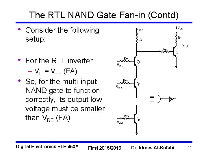
The RTL NAND Gate Fan-in (Contd) • Consider the following setup: VCC RC RC RB • • For the RTL inverter RB 1 VIN 1 Vout Q Q 1 – VIL = VBE (FA) So, for the multi-input NAND gate to function correctly, its output low voltage must be smaller than VBE (FA) Digital Electronics ELE 450 A RB 2 VIN 2 RBN VINN First 2015/2016 Q 2 QN Dr. Idrees Al-Kofahi 11

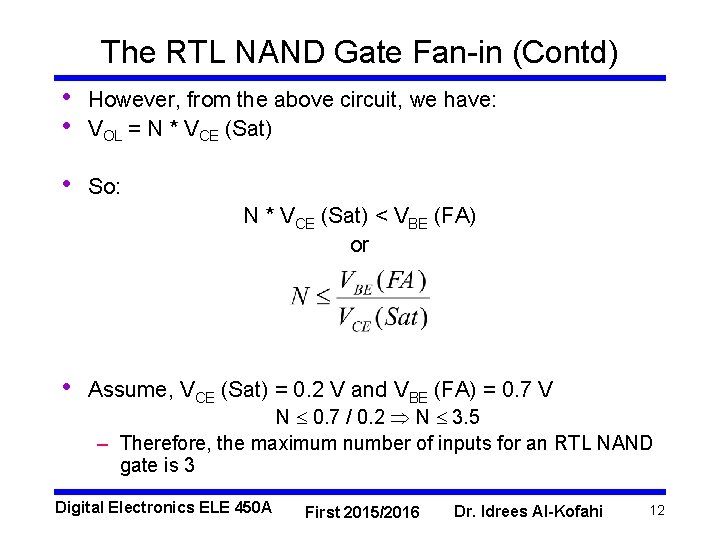
The RTL NAND Gate Fan-in (Contd) • • However, from the above circuit, we have: VOL = N * VCE (Sat) • So: N * VCE (Sat) < VBE (FA) or • Assume, VCE (Sat) = 0. 2 V and VBE (FA) = 0. 7 V N 0. 7 / 0. 2 N 3. 5 – Therefore, the maximum number of inputs for an RTL NAND gate is 3 Digital Electronics ELE 450 A First 2015/2016 Dr. Idrees Al-Kofahi 12

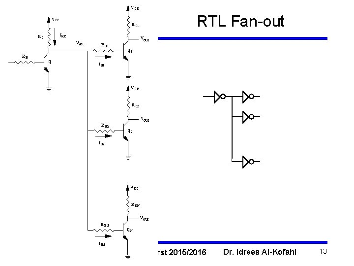
V CC RTL Fan-out V CC R C 1 IRC RC Vout RB Q Vout R B 1 Q 1 IB 1 V CC R C 2 Vout R B 2 Q 2 IB 2 V CC R CN Vout R BN QN IBN Digital Electronics ELE 450 A First 2015/2016 Dr. Idrees Al-Kofahi 13

RTL Fan-out – Output Low • We always consider the driving gate. • • When VIN of the driver is HIGH, its Vout = VCE(Sat) Given that VCE (Sat) < VBE (FA) Then all load transistors will be cut-off Therefore, IB 1 = IB 2 = … = IBN = 0 = IIL • So, the low state does not affect fan-out. Digital Electronics ELE 450 A First 2015/2016 Dr. Idrees Al-Kofahi 14

RTL Fan-out – Output High • When VIN of the driver is LOW, the transistor Q is cut-off and Vout = VCC • However, Vout is the VIN for each of the load transistors. • – Therefore, Q 1, Q 2, …, QN will all be saturated and taking current into their bases. – This will cause a non-zero IRC to flow. and Vout = VCC - IRC * RC Digital Electronics ELE 450 A First 2015/2016 Dr. Idrees Al-Kofahi 15

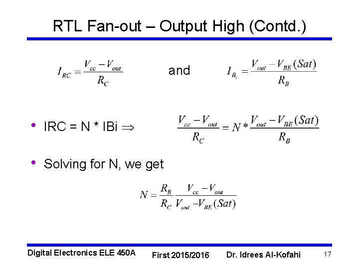
RTL Fan-out – Output High (Contd. ) • • Since IRC = N * IB then, the more gates connected to the output the bigger IRC becomes and the smaller Vout becomes. The limit on Fan-out is when Vout drops all the way down to VIH. At that point Q 1, Q 2, …, QN are at the edge of saturation. Adding more gates will drive the transistors out of saturation. Maximum Fan-out occurs when Vout ≥ VIH Digital Electronics ELE 450 A First 2015/2016 Dr. Idrees Al-Kofahi 16

RTL Fan-out – Output High (Contd. ) and • IRC = N * IBi • Solving for N, we get Digital Electronics ELE 450 A First 2015/2016 Dr. Idrees Al-Kofahi 17

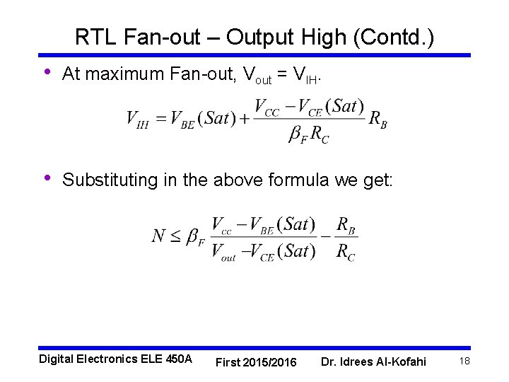
RTL Fan-out – Output High (Contd. ) • At maximum Fan-out, Vout = VIH. • Substituting in the above formula we get: Digital Electronics ELE 450 A First 2015/2016 Dr. Idrees Al-Kofahi 18

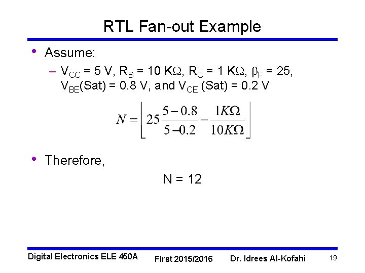
RTL Fan-out Example • Assume: – VCC = 5 V, RB = 10 KW, RC = 1 KW, b. F = 25, VBE(Sat) = 0. 8 V, and VCE (Sat) = 0. 2 V • Therefore, N = 12 Digital Electronics ELE 450 A First 2015/2016 Dr. Idrees Al-Kofahi 19

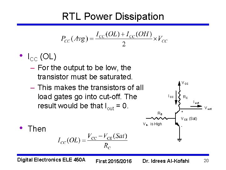
RTL Power Dissipation • ICC (OL) – For the output to be low, the transistor must be saturated. – This makes the transistors of all load gates go into cut-off. The result would be that Iout = 0. V CC I CC RC I out RB + V out V CE (Sat) • V in is High Then Digital Electronics ELE 450 A First 2015/2016 - Dr. Idrees Al-Kofahi 20

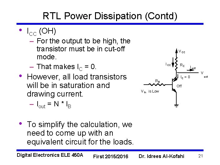
RTL Power Dissipation (Contd) • • ICC (OH) – For the output to be high, the transistor must be in cut-off mode. – That makes IC = 0. However, all load transistors will be in saturation and drawing current. V CC I CC RB RC IC = 0 I out V out Off V in is Low – Iout = N * IB • To simplify the calculation, we need to come up with an equivalent circuit for the loads. Digital Electronics ELE 450 A First 2015/2016 Dr. Idrees Al-Kofahi 21

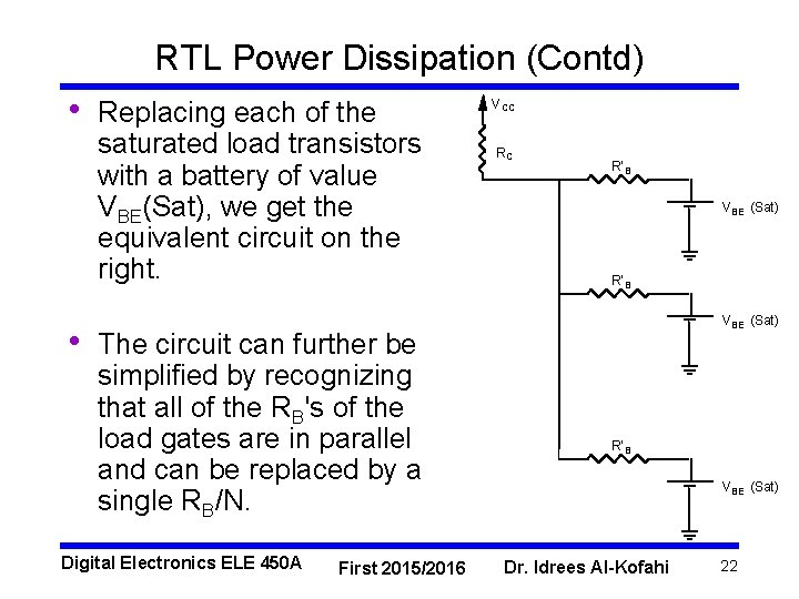
RTL Power Dissipation (Contd) • • Replacing each of the saturated load transistors with a battery of value VBE(Sat), we get the equivalent circuit on the right. The circuit can further be simplified by recognizing that all of the RB's of the load gates are in parallel and can be replaced by a single RB/N. Digital Electronics ELE 450 A First 2015/2016 V CC RC R' B VBE (Sat) Dr. Idrees Al-Kofahi 22

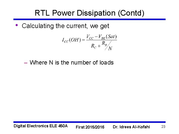
RTL Power Dissipation (Contd) • Calculating the current, we get – Where N is the number of loads Digital Electronics ELE 450 A First 2015/2016 Dr. Idrees Al-Kofahi 23

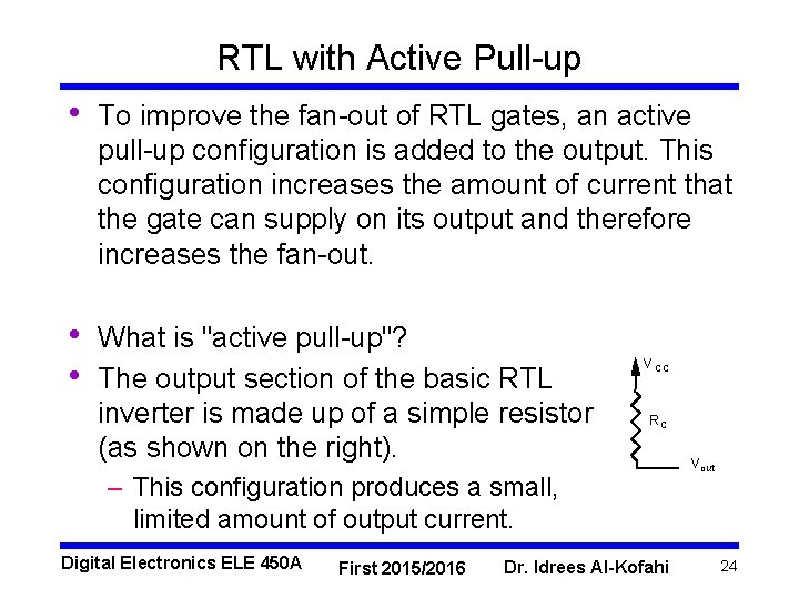
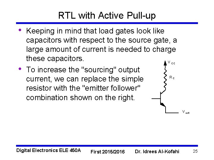
RTL with Active Pull-up • To improve the fan-out of RTL gates, an active pull-up configuration is added to the output. This configuration increases the amount of current that the gate can supply on its output and therefore increases the fan-out. • • What is "active pull-up"? The output section of the basic RTL inverter is made up of a simple resistor (as shown on the right). V CC RC – This configuration produces a small, limited amount of output current. Digital Electronics ELE 450 A First 2015/2016 Dr. Idrees Al-Kofahi V out 24

RTL with Active Pull-up • • Keeping in mind that load gates look like capacitors with respect to the source gate, a large amount of current is needed to charge these capacitors. V To increase the "sourcing" output R current, we can replace the simple resistor with the "emitter follower" combination shown on the right. CC C V out Digital Electronics ELE 450 A First 2015/2016 Dr. Idrees Al-Kofahi 25

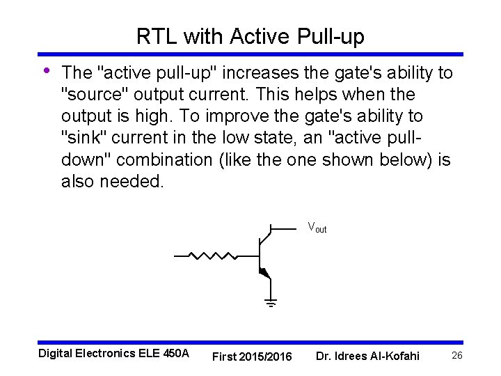
RTL with Active Pull-up • The "active pull-up" increases the gate's ability to "source" output current. This helps when the output is high. To improve the gate's ability to "sink" current in the low state, an "active pulldown" combination (like the one shown below) is also needed. Vout Digital Electronics ELE 450 A First 2015/2016 Dr. Idrees Al-Kofahi 26

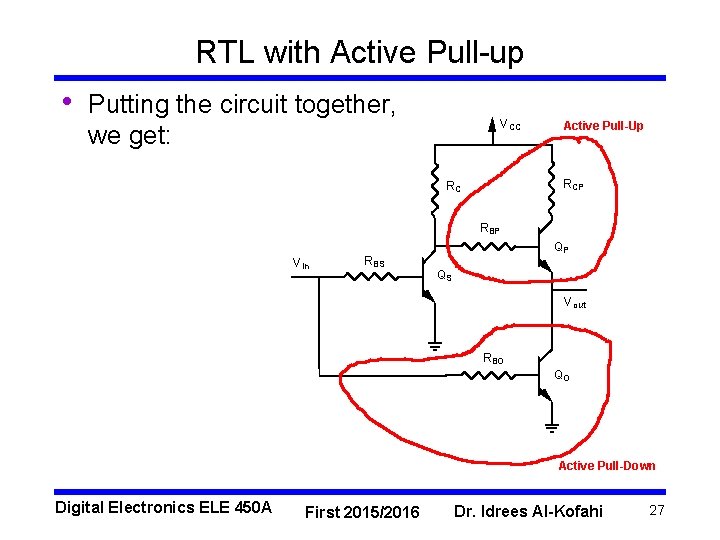
RTL with Active Pull-up • Putting the circuit together, we get: V CC Active Pull-Up R CP RC RBP V in RBS QP QS V out RBO QO Active Pull-Down Digital Electronics ELE 450 A First 2015/2016 Dr. Idrees Al-Kofahi 27

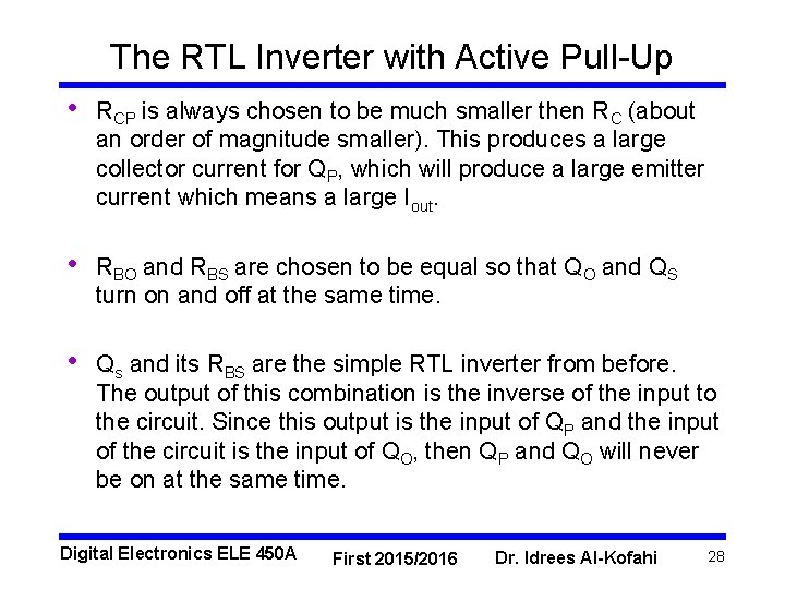
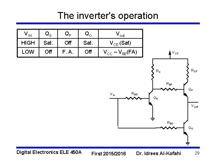
The RTL Inverter with Active Pull-Up • RCP is always chosen to be much smaller then RC (about an order of magnitude smaller). This produces a large collector current for QP, which will produce a large emitter current which means a large Iout. • RBO and RBS are chosen to be equal so that QO and QS turn on and off at the same time. • Qs and its RBS are the simple RTL inverter from before. The output of this combination is the inverse of the input to the circuit. Since this output is the input of QP and the input of the circuit is the input of QO, then QP and QO will never be on at the same time. Digital Electronics ELE 450 A First 2015/2016 Dr. Idrees Al-Kofahi 28

The inverter's operation VIN QS QP QO Vout HIGH Sat. Off Sat. VCE (Sat) LOW Off F. A. Off VCC – VBE(FA) V CC R CP RC RBP V in RBS QP QS V out RBO QO Digital Electronics ELE 450 A First 2015/2016 Dr. Idrees Al-Kofahi 29

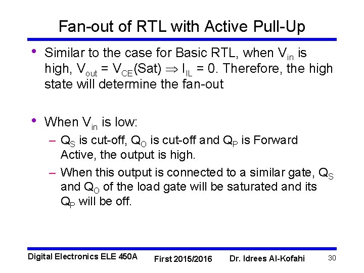
Fan-out of RTL with Active Pull-Up • Similar to the case for Basic RTL, when Vin is high, Vout = VCE(Sat) IIL = 0. Therefore, the high state will determine the fan-out • When Vin is low: – QS is cut-off, QO is cut-off and QP is Forward Active, the output is high. – When this output is connected to a similar gate, QS and QO of the load gate will be saturated and its QP will be off. Digital Electronics ELE 450 A First 2015/2016 Dr. Idrees Al-Kofahi 30

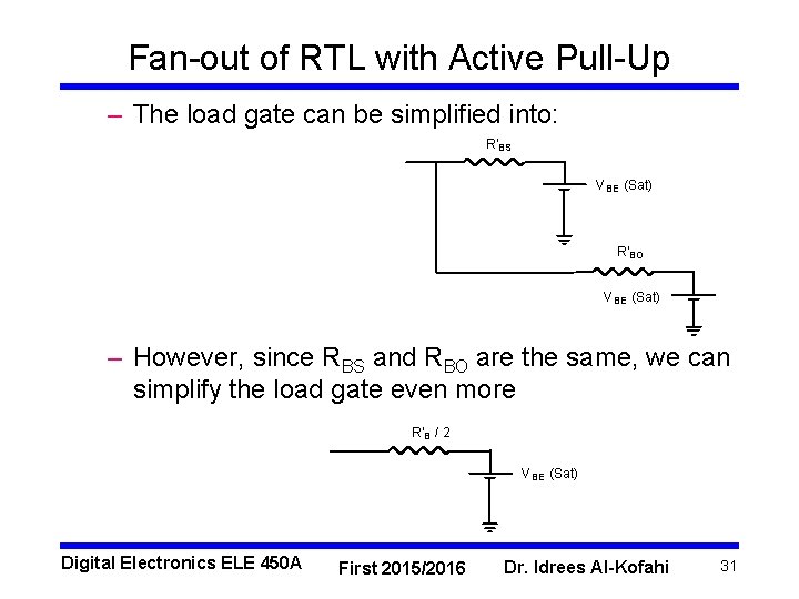
Fan-out of RTL with Active Pull-Up – The load gate can be simplified into: R'BS V BE (Sat) R'BO V BE (Sat) – However, since RBS and RBO are the same, we can simplify the load gate even more R'B / 2 V BE (Sat) Digital Electronics ELE 450 A First 2015/2016 Dr. Idrees Al-Kofahi 31

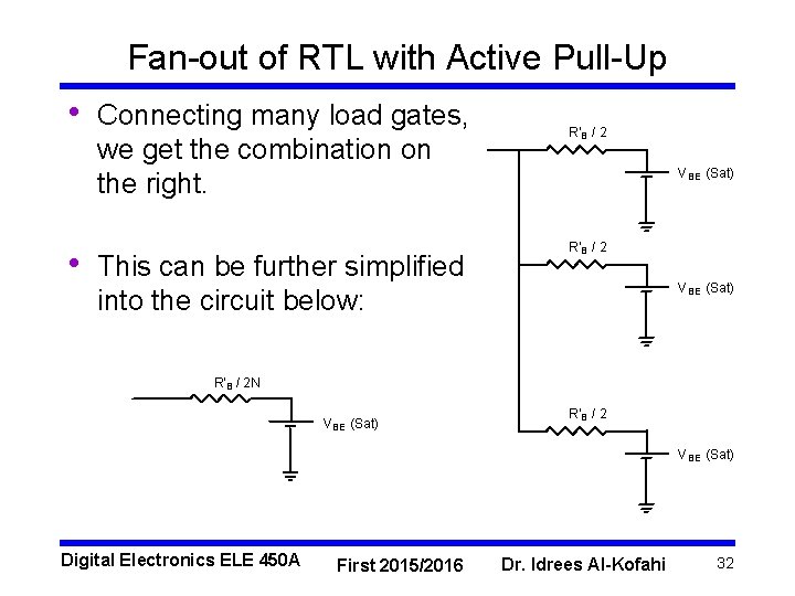
Fan-out of RTL with Active Pull-Up • • Connecting many load gates, we get the combination on the right. This can be further simplified into the circuit below: R'B / 2 V BE (Sat) R'B / 2 N VBE (Sat) R'B / 2 V BE (Sat) Digital Electronics ELE 450 A First 2015/2016 Dr. Idrees Al-Kofahi 32

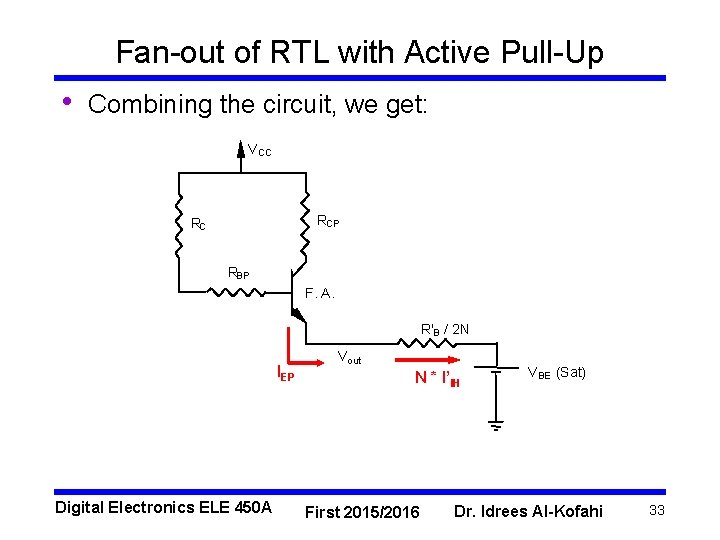
Fan-out of RTL with Active Pull-Up • Combining the circuit, we get: V CC RCP RC RBP F. A. R'B / 2 N IEP Digital Electronics ELE 450 A V out N * I’IH First 2015/2016 V BE (Sat) Dr. Idrees Al-Kofahi 33

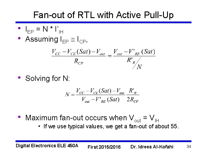
Fan-out of RTL with Active Pull-Up • • IEP = N * I’IH Assuming IEP ICP, • Solving for N: • Maximum fan-out occurs when Vout = VIH • If we use typical values, we get a fan-out of about 55. Digital Electronics ELE 450 A First 2015/2016 Dr. Idrees Al-Kofahi 34

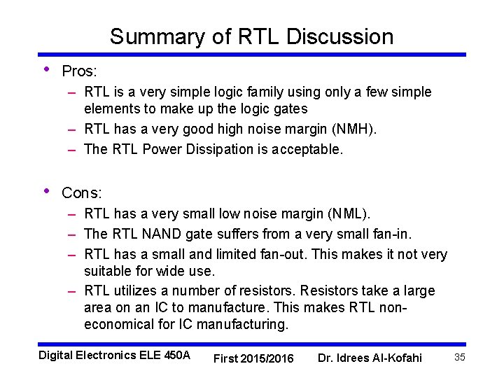
Summary of RTL Discussion • Pros: – RTL is a very simple logic family using only a few simple elements to make up the logic gates – RTL has a very good high noise margin (NMH). – The RTL Power Dissipation is acceptable. • Cons: – RTL has a very small low noise margin (NML). – The RTL NAND gate suffers from a very small fan-in. – RTL has a small and limited fan-out. This makes it not very suitable for wide use. – RTL utilizes a number of resistors. Resistors take a large area on an IC to manufacture. This makes RTL noneconomical for IC manufacturing. Digital Electronics ELE 450 A First 2015/2016 Dr. Idrees Al-Kofahi 35