CHAPTER 5 INTRODUCTION TO TRANSISTOR 5 1 TRANSISTOR


:")


- Slides: 15
CHAPTER -5 INTRODUCTION TO TRANSISTOR
5. 1 TRANSISTOR CONSTRUCTION, TYPES OF TRANSISTOR, TRANSISTOR OPERATION AND AMPLIFYING ACTION
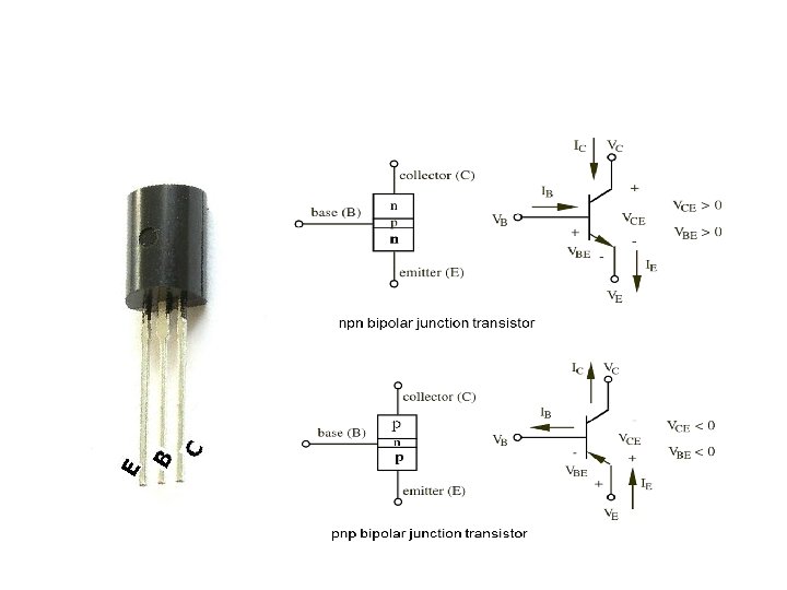
Transistor construction • 3 adjacent regions of doped Si (each connected to a lead): – Base. (thin layer, less doped). – Collector. – Emitter. • 2 types of BJT: – NPN. – PNP. • Most common: NPN
• 1 thin layer of p-type, sandwiched between 2 layers of n-type. • N-type of emitter: more heavily doped than collector. • With VC>VB>VE: – Base-Emitter junction forward biased, Base-Collector reverse biased. – Electrons diffuse from Emitter to Base (from n to p). – There’s a depletion layer on the Base-Collector junction no flow of e- allowed. – But the Base is thin and Emitter region is n+ (heavily doped) electrons have enough momentum to cross the Base into the Collector. – The small base current IB controls a large current IC
NPN transistor operation
NPN Transistor Connection
• 1 thin layer of p-type, sandwiched between 2 layers of n-type. • N-type of emitter: more heavily doped than collector. • With VC>VB>VE: – Base-Emitter junction forward biased, Base-Collector reverse biased. – Electrons diffuse from Emitter to Base (from n to p). – There’s a depletion layer on the Base-Collector junction no flow of e- allowed. – the Base is thin and Emitter region is n+ (heavily doped) electrons have enough momentum to cross the Base into the Collector. – The small base current IB controls a large current IC
LEACKAGE CURRENT • it is primarily caused by electronic devices such as transistors or diodes, which conduct a small amount of current even when they are turned off. • It is because of minority charge carrier. • Even though this off current is an order of magnitude less than the current through the device when it is on.
TRANSISTOR AS AN AMPLIFIER NPN CE AMPLIFIER I/P & O/P WAVEFORMS
• The common emitter transistor amplifier is the only configuration that gives an inversion, 180°, between the input and output signals. • The reason for this can be seen from the fact that as the input voltage rises, so the current increases through the base circuit. In turn this increases the current thought the collector circuit, i. e. it tends to turn the transistor on. • This results in the voltage between the collector and emitter terminals falling. • In this way an increase in voltage between the base and emitter has resulted in a fall in voltage between the collector and emitter terminals, in other words the phase of the two signals has been inverted.
• CIN, COUT These capacitors provide AC coupling between stages. . • R 1, R 2 These resistors provide the bias for the base of the transistor. • R 3 This is the collector load resistor within the common emitter amplifier. • R 4 This resistor in the common emitter amplifier provides a measure of DC feedback • CE This is a bypass capacitor. The effect of R 4 is to reduce the gain of the circuit. Bypassing the resistor enables greater levels of AC gain to be achieved.
Transistor configuration
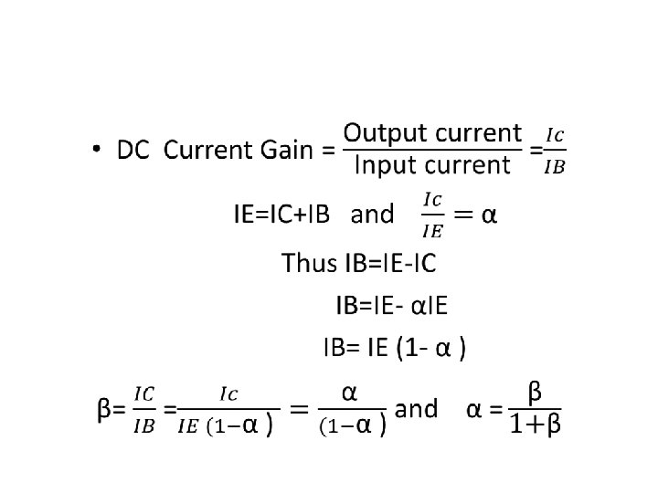
Relation between current gain, α and β • Current Gain: – α is the fraction of electrons that diffuse across the narrow Base region – 1 - α is the fraction of electrons that recombine with holes in the Base region to create base current • The current Gain is expressed in terms of the β (beta) of the transistor (often called hfe by manufacturers). • β (beta) is Temperature and Voltage dependent. • It can vary a lot among transistors (common values for signal BJT: 20 - 200).