Chapter 5 Digital Design and Computer Architecture ARM



![Counter Verilog (FSM style) module counter (input logic clk, reset, output logic [N-1: 0] Counter Verilog (FSM style) module counter (input logic clk, reset, output logic [N-1: 0]](https://slidetodoc.com/presentation_image_h/12c3020cb65ee3a249a5d7ec9fa9271e/image-77.jpg)
![Counter Verilog (better idiom) module counter (input logic clk, reset, output logic [N-1: 0] Counter Verilog (better idiom) module counter (input logic clk, reset, output logic [N-1: 0]](https://slidetodoc.com/presentation_image_h/12c3020cb65ee3a249a5d7ec9fa9271e/image-78.jpg)
![Shift Register Verilog Idiom module shiftreg(input logic [N-1: 0] output logic always_ff @(posedge clk) Shift Register Verilog Idiom module shiftreg(input logic [N-1: 0] output logic always_ff @(posedge clk)](https://slidetodoc.com/presentation_image_h/12c3020cb65ee3a249a5d7ec9fa9271e/image-83.jpg)

- Slides: 126

Chapter 5 Digital Design and Computer Architecture: ARM® Edition Sarah L. Harris and David Money Harris Digital Design and Computer Architecture: ARM® Edition © 2015 Chapter 5 <1>

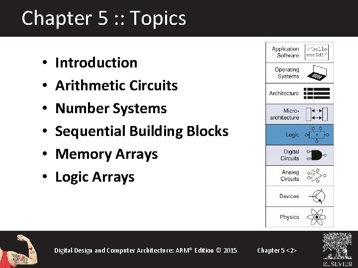
Chapter 5 : : Topics • • • Introduction Arithmetic Circuits Number Systems Sequential Building Blocks Memory Arrays Logic Arrays Digital Design and Computer Architecture: ARM® Edition © 2015 Chapter 5 <2>

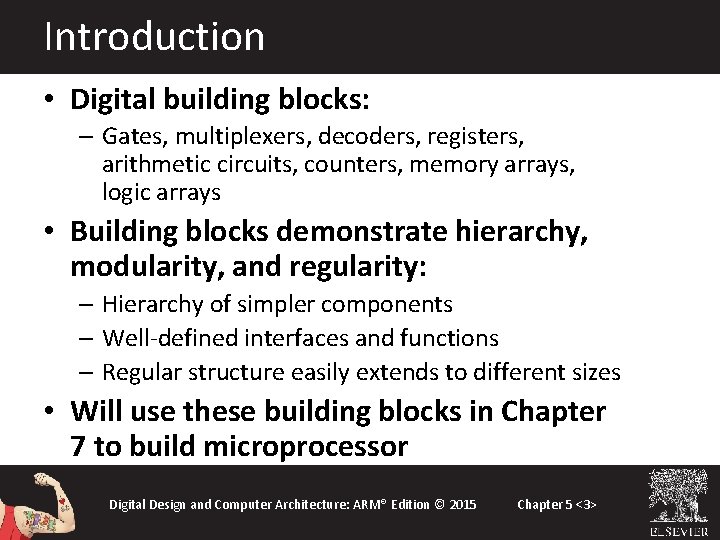
Introduction • Digital building blocks: – Gates, multiplexers, decoders, registers, arithmetic circuits, counters, memory arrays, logic arrays • Building blocks demonstrate hierarchy, modularity, and regularity: – Hierarchy of simpler components – Well-defined interfaces and functions – Regular structure easily extends to different sizes • Will use these building blocks in Chapter 7 to build microprocessor Digital Design and Computer Architecture: ARM® Edition © 2015 Chapter 5 <3>

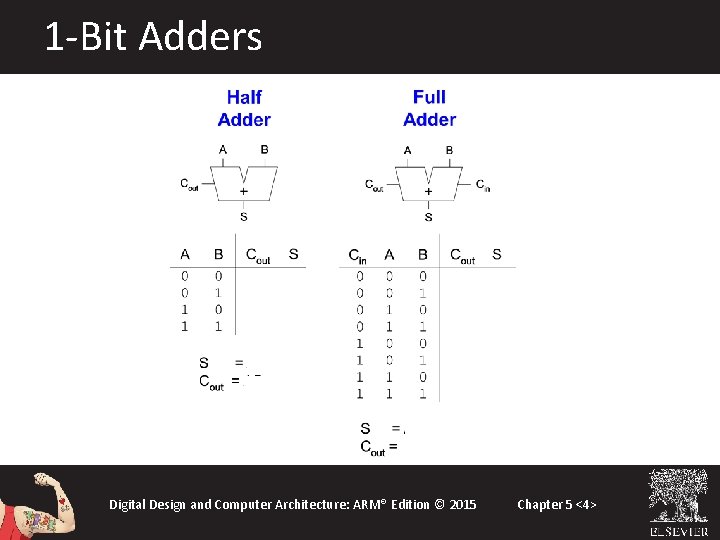
1 -Bit Adders Digital Design and Computer Architecture: ARM® Edition © 2015 Chapter 5 <4>

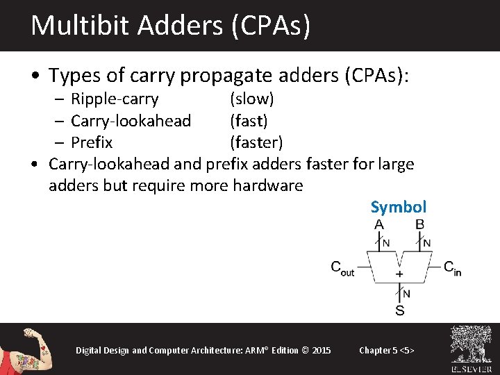
Multibit Adders (CPAs) • Types of carry propagate adders (CPAs): – Ripple-carry (slow) – Carry-lookahead (fast) – Prefix (faster) • Carry-lookahead and prefix adders faster for large adders but require more hardware Symbol Digital Design and Computer Architecture: ARM® Edition © 2015 Chapter 5 <5>

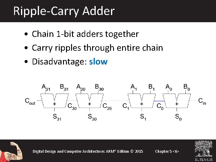
Ripple-Carry Adder • Chain 1 -bit adders together • Carry ripples through entire chain • Disadvantage: slow Digital Design and Computer Architecture: ARM® Edition © 2015 Chapter 5 <6>

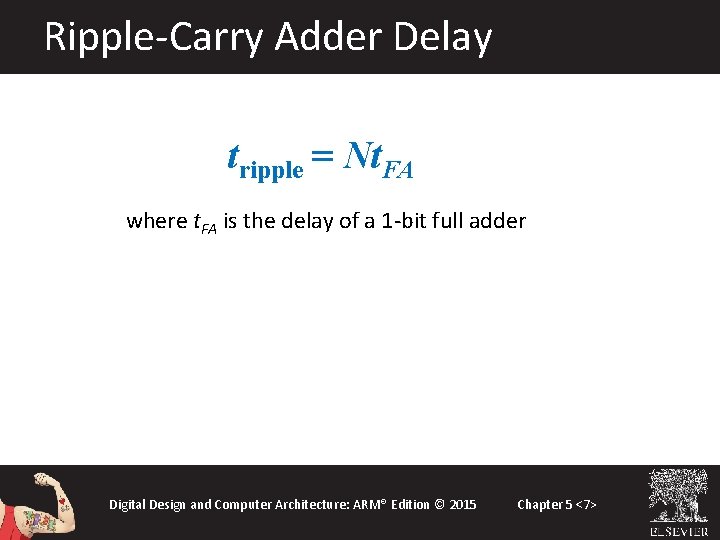
Ripple-Carry Adder Delay tripple = Nt. FA where t. FA is the delay of a 1 -bit full adder Digital Design and Computer Architecture: ARM® Edition © 2015 Chapter 5 <7>

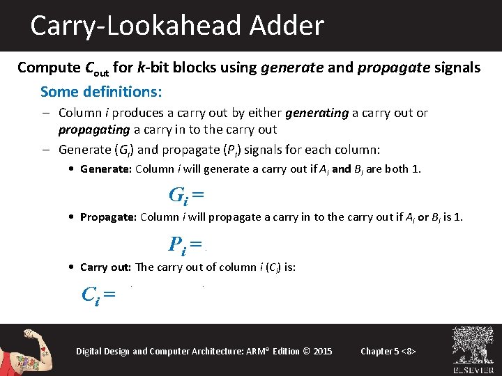
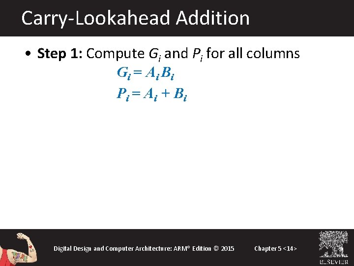
Carry-Lookahead Adder Compute Cout for k-bit blocks using generate and propagate signals Some definitions: – Column i produces a carry out by either generating a carry out or propagating a carry in to the carry out – Generate (Gi) and propagate (Pi) signals for each column: • Generate: Column i will generate a carry out if Ai and Bi are both 1. Gi = A i B i • Propagate: Column i will propagate a carry in to the carry out if Ai or Bi is 1. Pi = Ai + Bi • Carry out: The carry out of column i (Ci) is: Ci = Ai Bi + (Ai + Bi )Ci-1 = Gi + Pi Ci-1 Digital Design and Computer Architecture: ARM® Edition © 2015 Chapter 5 <8>

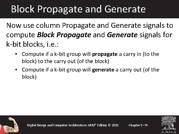
Block Propagate and Generate Now use column Propagate and Generate signals to compute Block Propagate and Generate signals for k-bit blocks, i. e. : • Compute if a k-bit group will propagate a carry in (to the block) to the carry out (of the block) • Compute if a k-bit group will generate a carry out (of the block) Digital Design and Computer Architecture: ARM® Edition © 2015 Chapter 5 <9>

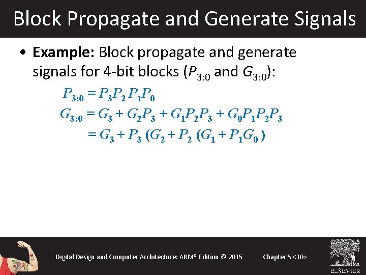
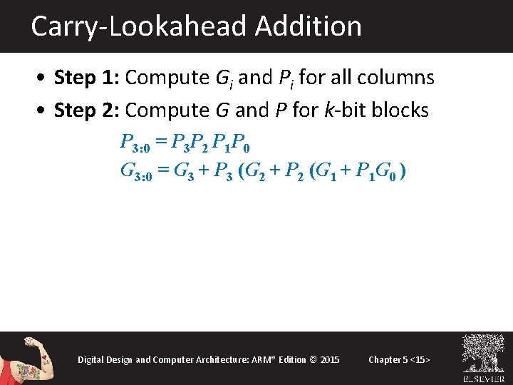
Block Propagate and Generate Signals • Example: Block propagate and generate signals for 4 -bit blocks (P 3: 0 and G 3: 0): P 3: 0 = P 3 P 2 P 1 P 0 G 3: 0 = G 3 + G 2 P 3 + G 1 P 2 P 3 + G 0 P 1 P 2 P 3 = G 3 + P 3 (G 2 + P 2 (G 1 + P 1 G 0 ) Digital Design and Computer Architecture: ARM® Edition © 2015 Chapter 5 <10>

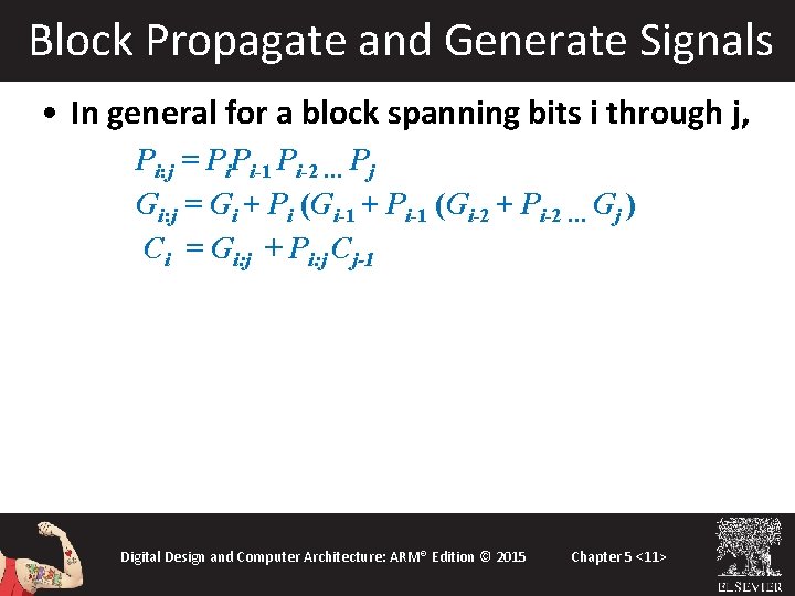
Block Propagate and Generate Signals • In general for a block spanning bits i through j, Pi: j = Pi. Pi-1 Pi-2 … Pj Gi: j = Gi + Pi (Gi-1 + Pi-1 (Gi-2 + Pi-2 … Gj ) Ci = Gi: j + Pi: j Cj-1 Digital Design and Computer Architecture: ARM® Edition © 2015 Chapter 5 <11>

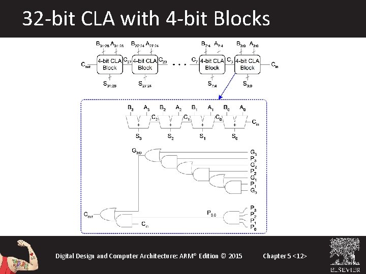
32 -bit CLA with 4 -bit Blocks Digital Design and Computer Architecture: ARM® Edition © 2015 Chapter 5 <12>

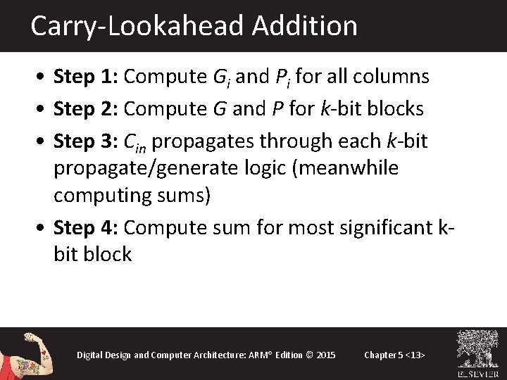
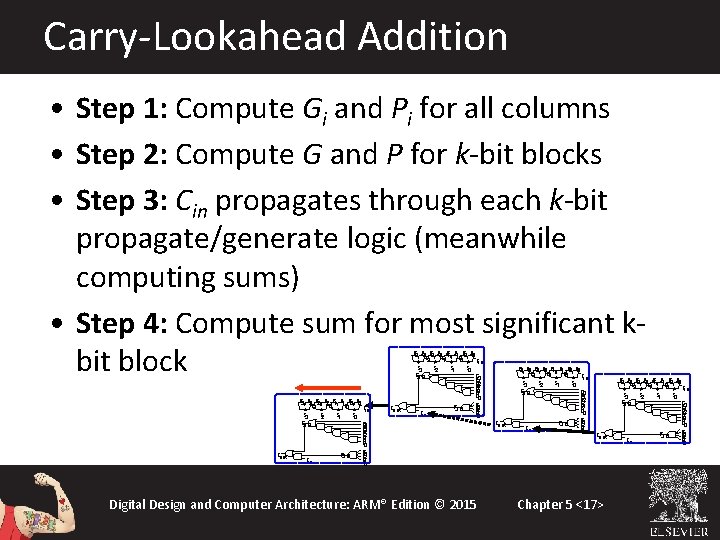
Carry-Lookahead Addition • Step 1: Compute Gi and Pi for all columns • Step 2: Compute G and P for k-bit blocks • Step 3: Cin propagates through each k-bit propagate/generate logic (meanwhile computing sums) • Step 4: Compute sum for most significant kbit block Digital Design and Computer Architecture: ARM® Edition © 2015 Chapter 5 <13>

Carry-Lookahead Addition • Step 1: Compute Gi and Pi for all columns Gi = A i B i Pi = Ai + Bi Digital Design and Computer Architecture: ARM® Edition © 2015 Chapter 5 <14>

Carry-Lookahead Addition • Step 1: Compute Gi and Pi for all columns • Step 2: Compute G and P for k-bit blocks P 3: 0 = P 3 P 2 P 1 P 0 G 3: 0 = G 3 + P 3 (G 2 + P 2 (G 1 + P 1 G 0 ) Digital Design and Computer Architecture: ARM® Edition © 2015 Chapter 5 <15>

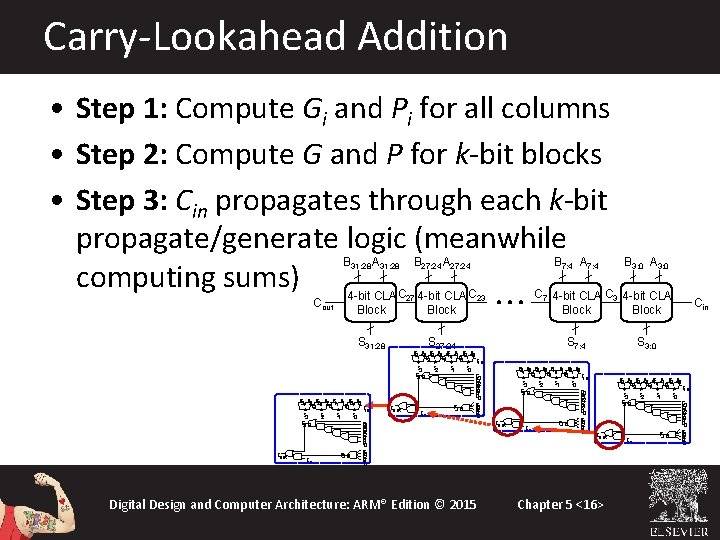
Carry-Lookahead Addition • Step 1: Compute Gi and Pi for all columns • Step 2: Compute G and P for k-bit blocks • Step 3: Cin propagates through each k-bit propagate/generate logic (meanwhile computing sums) B 31: 28 A 31: 28 Cout B 7: 4 A 7: 4 4 -bit CLA C 27 4 -bit CLA C 23 Block S 31: 28 Cout B 27: 24 A 27: 24 B 3 A 3 B 2 A 2 B 1 A 1 B 0 A 0 C C C + 2 + 1 + 0 + Cin S 3 S 2 S 1 S 0 G 3: 0 G 3 P 3 G 2 P 2 G 1 P 1 G 0 P 3: 0 P 2 P Cin P 1 0 C 7 4 -bit CLA C 3 4 -bit CLA Block S 27: 24 Cout S 7: 4 B 3 A 3 B 2 A 2 B 1 A 1 B 0 A 0 C C C + 2 + 1 + 0 + Cin S 3 S 2 S 1 S 0 G 3: 0 G 3 P 3 G 2 P 2 G 1 P 1 G 0 P 3: 0 P 2 P 1 Cin P 0 Digital Design and Computer Architecture: ARM® Edition © 2015 B 3: 0 A 3: 0 Cout B 3 A 3 B 2 A 2 B 1 A 1 B 0 A 0 C C C + 2 + 1 + 0 + Cin S 3 S 2 S 1 S 0 G 3: 0 G 3 P 3 G 2 P 2 G 1 P 1 G 0 P 3: 0 P 2 P Cin P 1 0 S 3: 0 Cout Chapter 5 <16> B 3 A 3 B 2 A 2 B 1 A 1 B 0 A 0 C C C + 2 + 1 + 0 + Cin S 3 S 2 S 1 S 0 G 3: 0 G 3 P 3 G 2 P 2 G 1 P 1 G 0 P 3: 0 P 2 P Cin P 1 0 Cin

Carry-Lookahead Addition • Step 1: Compute Gi and Pi for all columns • Step 2: Compute G and P for k-bit blocks • Step 3: Cin propagates through each k-bit propagate/generate logic (meanwhile computing sums) • Step 4: Compute sum for most significant kbit block Cout B 3 A 3 B 2 A 2 B 1 A 1 B 0 A 0 C C C + 2 + 1 + 0 + Cin S 3 S 2 S 1 S 0 G 3: 0 G 3 P 3 G 2 P 2 G 1 P 1 G 0 P 3: 0 P 2 P Cin P 1 0 Cout B 3 A 3 B 2 A 2 B 1 A 1 B 0 A 0 C C C + 2 + 1 + 0 + Cin S 3 S 2 S 1 S 0 G 3: 0 G 3 P 3 G 2 P 2 G 1 P 1 G 0 P 3: 0 P 2 P 1 Cin P 0 Digital Design and Computer Architecture: ARM® Edition © 2015 Cout B 3 A 3 B 2 A 2 B 1 A 1 B 0 A 0 C C C + 2 + 1 + 0 + Cin S 3 S 2 S 1 S 0 G 3: 0 G 3 P 3 G 2 P 2 G 1 P 1 G 0 P 3: 0 P 2 P Cin P 1 0 Cout Chapter 5 <17> B 3 A 3 B 2 A 2 B 1 A 1 B 0 A 0 C C C + 2 + 1 + 0 + Cin S 3 S 2 S 1 S 0 G 3: 0 G 3 P 3 G 2 P 2 G 1 P 1 G 0 P 3: 0 P 2 P Cin P 1 0

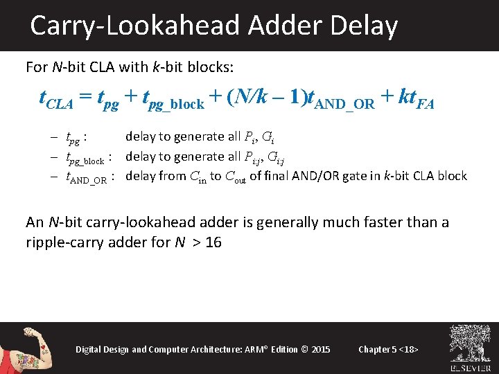
Carry-Lookahead Adder Delay For N-bit CLA with k-bit blocks: t. CLA = tpg + tpg_block + (N/k – 1)t. AND_OR + kt. FA – tpg : delay to generate all Pi, Gi – tpg_block : delay to generate all Pi: j, Gi: j – t. AND_OR : delay from Cin to Cout of final AND/OR gate in k-bit CLA block An N-bit carry-lookahead adder is generally much faster than a ripple-carry adder for N > 16 Digital Design and Computer Architecture: ARM® Edition © 2015 Chapter 5 <18>

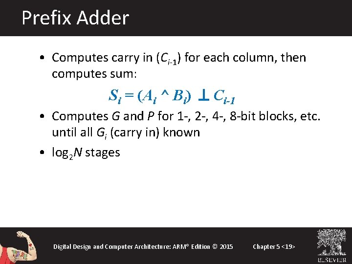
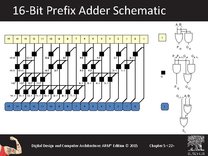
Prefix Adder • Computes carry in (Ci-1) for each column, then computes sum: Si = (Ai ^ Bi) ^ Ci-1 • Computes G and P for 1 -, 2 -, 4 -, 8 -bit blocks, etc. until all Gi (carry in) known • log 2 N stages Digital Design and Computer Architecture: ARM® Edition © 2015 Chapter 5 <19>

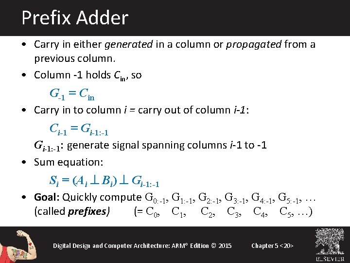
Prefix Adder • Carry in either generated in a column or propagated from a previous column. • Column -1 holds Cin, so G-1 = Cin • Carry in to column i = carry out of column i-1: Ci-1 = Gi-1: -1: generate signal spanning columns i-1 to -1 • Sum equation: Si = (Ai ^ Bi) ^ Gi-1: -1 • Goal: Quickly compute G 0: -1, G 1: -1, G 2: -1, G 3: -1, G 4: -1, G 5: -1, … (called prefixes) (= C 0, C 1, C 2, C 3, C 4, C 5, …) Digital Design and Computer Architecture: ARM® Edition © 2015 Chapter 5 <20>

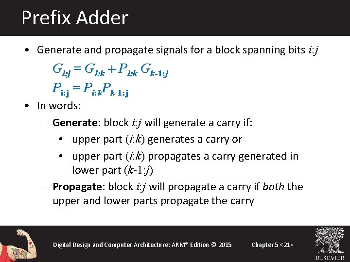
Prefix Adder • Generate and propagate signals for a block spanning bits i: j Gi: j = Gi: k + Pi: k Gk-1: j Pi: j = Pi: k. Pk-1: j • In words: – Generate: block i: j will generate a carry if: • upper part (i: k) generates a carry or • upper part (i: k) propagates a carry generated in lower part (k-1: j) – Propagate: block i: j will propagate a carry if both the upper and lower parts propagate the carry Digital Design and Computer Architecture: ARM® Edition © 2015 Chapter 5 <21>

16 -Bit Prefix Adder Schematic A i Bi 15 14 13 12 11 10 9 8 7 6 5 4 3 2 1 0 -1 i P i: i 14: 13 14: 11 12: 11 10: 9 13: 11 8: 7 10: 7 6: 5 9: 7 4: 3 6: 3 2: 1 5: 3 Pi: k Pk-1: j Gi: k 0: -1 2: -1 G i: i 1: -1 i: j 14: 7 13: 7 12: 7 11: 7 6: -1 5: -1 4: -1 3: -1 Pi: j 14: -1 15 13: -1 14 12: -1 13 11: -1 12 10: -1 11 9: -1 10 8: -1 9 Gi-1: -1 Ai Bi 7: -1 8 Gi: j 7 6 5 4 3 2 1 0 i Si Digital Design and Computer Architecture: ARM® Edition © 2015 Chapter 5 <22> Gk-1: j

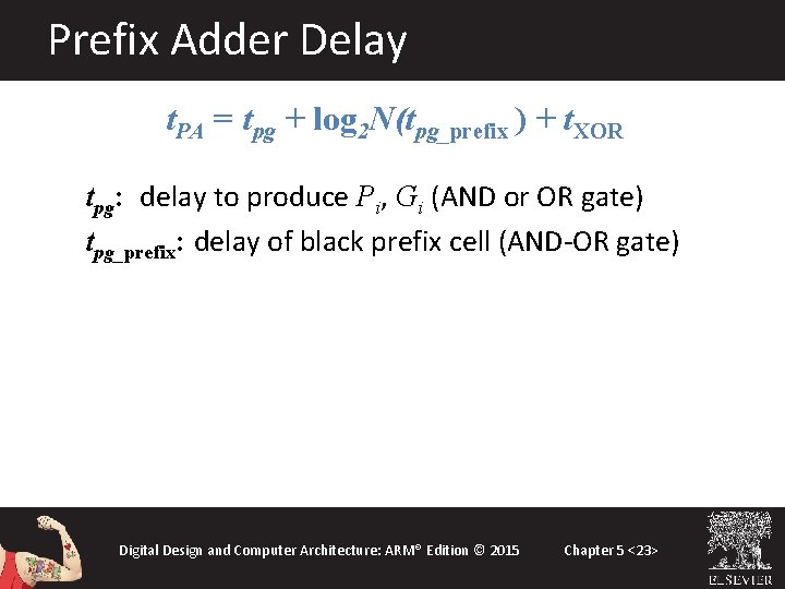
Prefix Adder Delay t. PA = tpg + log 2 N(tpg_prefix ) + t. XOR tpg: delay to produce Pi, Gi (AND or OR gate) tpg_prefix: delay of black prefix cell (AND-OR gate) Digital Design and Computer Architecture: ARM® Edition © 2015 Chapter 5 <23>

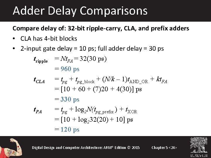
Adder Delay Comparisons Compare delay of: 32 -bit ripple-carry, CLA, and prefix adders • CLA has 4 -bit blocks • 2 -input gate delay = 10 ps; full adder delay = 30 ps tripple = Nt. FA = 32(30 ps) = 960 ps t. CLA = tpg + tpg_block + (N/k – 1)t. AND_OR + kt. FA = [10 + 60 + (7)20 + 4(30)] ps = 330 ps t. PA = tpg + log 2 N(tpg_prefix ) + t. XOR = [10 + log 232(20) + 10] ps = 120 ps Digital Design and Computer Architecture: ARM® Edition © 2015 Chapter 5 <24>

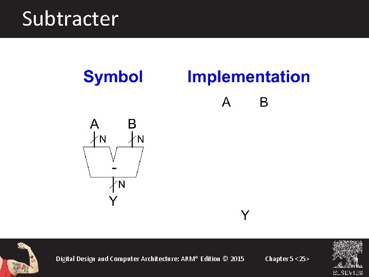
Subtracter Digital Design and Computer Architecture: ARM® Edition © 2015 Chapter 5 <25>

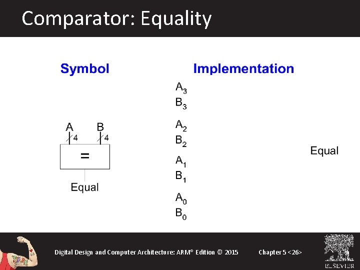
Comparator: Equality Digital Design and Computer Architecture: ARM® Edition © 2015 Chapter 5 <26>

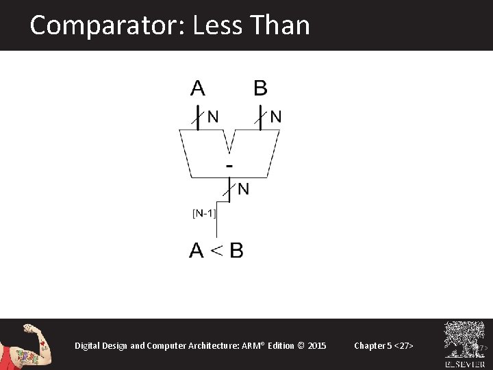
Comparator: Less Than Digital Design and Computer Architecture: ARM® Edition © 2015 Chapter 5 <27> 5 -<27>

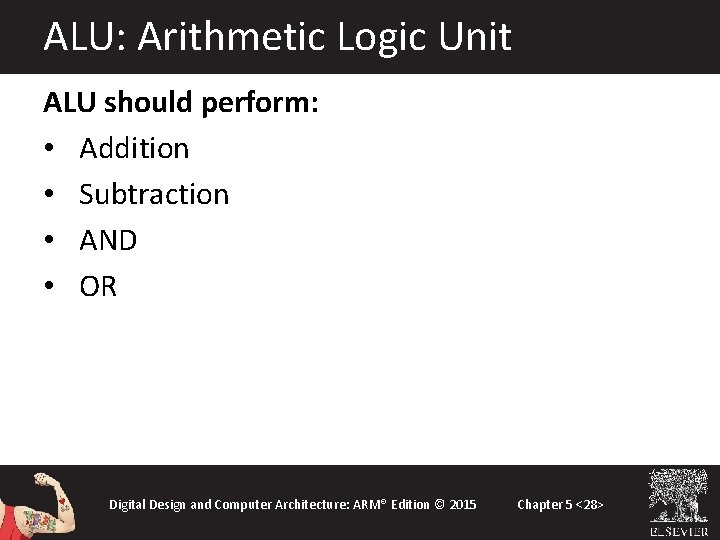
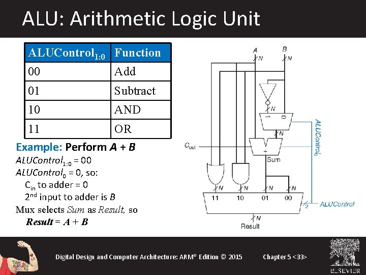
ALU: Arithmetic Logic Unit ALU should perform: • Addition • Subtraction • AND • OR Digital Design and Computer Architecture: ARM® Edition © 2015 Chapter 5 <28>

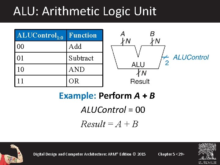
ALU: Arithmetic Logic Unit ALUControl 1: 0 Function 00 Add 01 Subtract 10 AND 11 OR Example: Perform A + B ALUControl = 00 Result = A + B Digital Design and Computer Architecture: ARM® Edition © 2015 Chapter 5 <29>

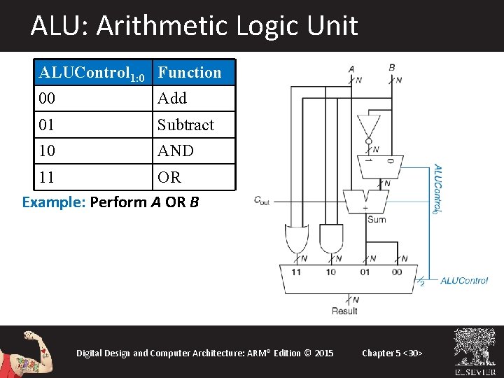
ALU: Arithmetic Logic Unit ALUControl 1: 0 Function 00 Add 01 Subtract 10 AND 11 OR Example: Perform A OR B Digital Design and Computer Architecture: ARM® Edition © 2015 Chapter 5 <30>

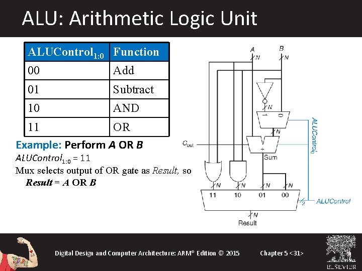
ALU: Arithmetic Logic Unit ALUControl 1: 0 Function 00 Add 01 Subtract 10 AND 11 OR Example: Perform A OR B ALUControl 1: 0 = 11 Mux selects output of OR gate as Result, so Result = A OR B Digital Design and Computer Architecture: ARM® Edition © 2015 Chapter 5 <31>

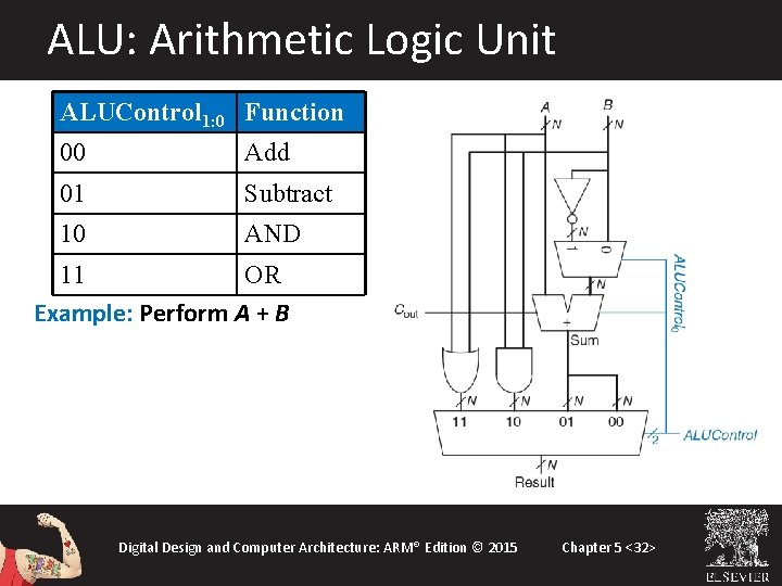
ALU: Arithmetic Logic Unit ALUControl 1: 0 Function 00 Add 01 Subtract 10 AND 11 OR Example: Perform A + B Digital Design and Computer Architecture: ARM® Edition © 2015 Chapter 5 <32>

ALU: Arithmetic Logic Unit ALUControl 1: 0 Function 00 Add 01 Subtract 10 AND 11 OR Example: Perform A + B ALUControl 1: 0 = 00 ALUControl 0 = 0, so: Cin to adder = 0 2 nd input to adder is B Mux selects Sum as Result, so Result = A + B Digital Design and Computer Architecture: ARM® Edition © 2015 Chapter 5 <33>

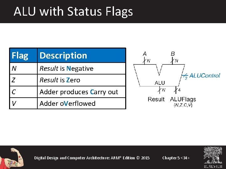
ALU with Status Flag Description N Result is Negative Z Result is Zero C Adder produces Carry out V Adder o. Verflowed Digital Design and Computer Architecture: ARM® Edition © 2015 Chapter 5 <34>

ALU with Status Flags Digital Design and Computer Architecture: ARM® Edition © 2015 Chapter 5 <35>

ALU with Status Flags: Negative N = 1 if: Result is negative So, N is connected to most significant bit of Result Digital Design and Computer Architecture: ARM® Edition © 2015 Chapter 5 <36>

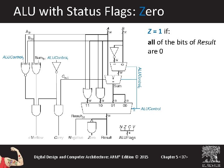
ALU with Status Flags: Zero Z = 1 if: all of the bits of Result are 0 Digital Design and Computer Architecture: ARM® Edition © 2015 Chapter 5 <37>

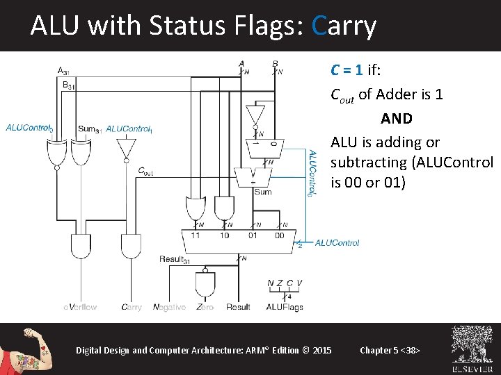
ALU with Status Flags: Carry C = 1 if: Cout of Adder is 1 AND ALU is adding or subtracting (ALUControl is 00 or 01) Digital Design and Computer Architecture: ARM® Edition © 2015 Chapter 5 <38>

ALU with Status Flags: o. Verflow V = 1 if: The addition of 2 samesigned numbers produces a result with the opposite sign Digital Design and Computer Architecture: ARM® Edition © 2015 Chapter 5 <39>

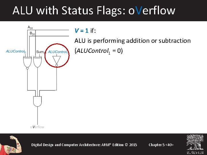
ALU with Status Flags: o. Verflow V = 1 if: ALU is performing addition or subtraction (ALUControl 1 = 0) Digital Design and Computer Architecture: ARM® Edition © 2015 Chapter 5 <40>

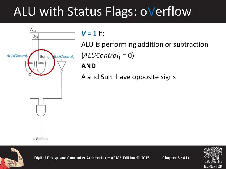
ALU with Status Flags: o. Verflow V = 1 if: ALU is performing addition or subtraction (ALUControl 1 = 0) AND A and Sum have opposite signs Digital Design and Computer Architecture: ARM® Edition © 2015 Chapter 5 <41>

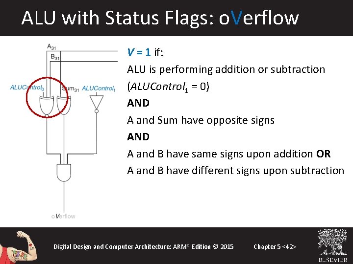
ALU with Status Flags: o. Verflow V = 1 if: ALU is performing addition or subtraction (ALUControl 1 = 0) AND A and Sum have opposite signs AND A and B have same signs upon addition OR A and B have different signs upon subtraction Digital Design and Computer Architecture: ARM® Edition © 2015 Chapter 5 <42>

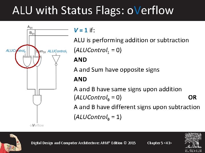
ALU with Status Flags: o. Verflow V = 1 if: ALU is performing addition or subtraction (ALUControl 1 = 0) AND A and Sum have opposite signs AND A and B have same signs upon addition (ALUControl 0 = 0) OR A and B have different signs upon subtraction (ALUControl 0 = 1) Digital Design and Computer Architecture: ARM® Edition © 2015 Chapter 5 <43>

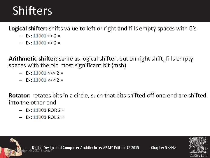
Shifters Logical shifter: shifts value to left or right and fills empty spaces with 0’s – Ex: 11001 >> 2 = 00110 – Ex: 11001 << 2 = 00100 Arithmetic shifter: same as logical shifter, but on right shift, fills empty spaces with the old most significant bit (msb) – Ex: 11001 >>> 2 = 11110 – Ex: 11001 <<< 2 = 00100 Rotator: rotates bits in a circle, such that bits shifted off one end are shifted into the other end – Ex: 11001 ROR 2 = 01110 – Ex: 11001 ROL 2 = 00111 Digital Design and Computer Architecture: ARM® Edition © 2015 Copyright © 2007 Elsevier Chapter 5 <44> 5 -<44>

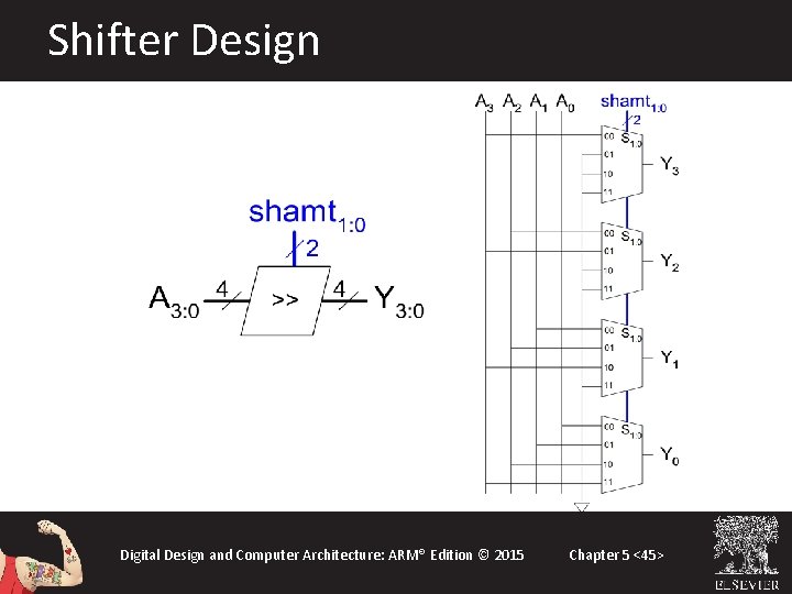
Shifter Design Digital Design and Computer Architecture: ARM® Edition © 2015 Chapter 5 <45>

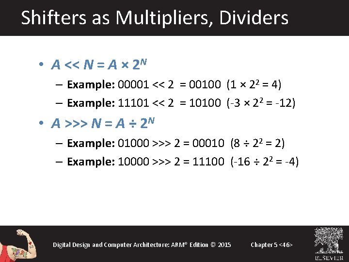
Shifters as Multipliers, Dividers • A << N = A × 2 N – Example: 00001 << 2 = 00100 (1 × 22 = 4) – Example: 11101 << 2 = 10100 (-3 × 22 = -12) • A >>> N = A ÷ 2 N – Example: 01000 >>> 2 = 00010 (8 ÷ 22 = 2) – Example: 10000 >>> 2 = 11100 (-16 ÷ 22 = -4) Digital Design and Computer Architecture: ARM® Edition © 2015 Chapter 5 <46>

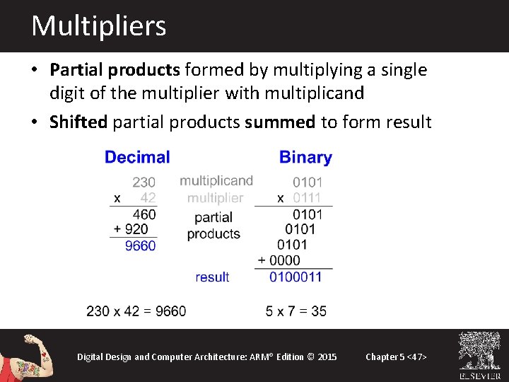
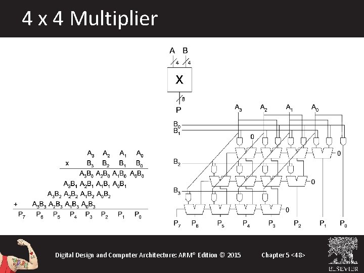
Multipliers • Partial products formed by multiplying a single digit of the multiplier with multiplicand • Shifted partial products summed to form result Digital Design and Computer Architecture: ARM® Edition © 2015 Chapter 5 <47>

4 x 4 Multiplier Digital Design and Computer Architecture: ARM® Edition © 2015 Chapter 5 <48>

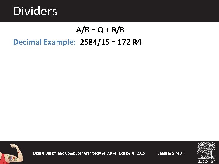
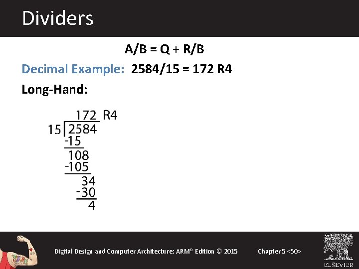
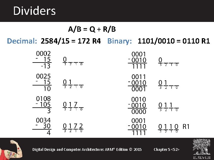
Dividers A/B = Q + R/B Decimal Example: 2584/15 = 172 R 4 Digital Design and Computer Architecture: ARM® Edition © 2015 Chapter 5 <49>

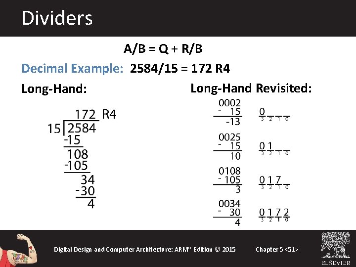
Dividers A/B = Q + R/B Decimal Example: 2584/15 = 172 R 4 Long-Hand: Digital Design and Computer Architecture: ARM® Edition © 2015 Chapter 5 <50>

Dividers A/B = Q + R/B Decimal Example: 2584/15 = 172 R 4 Long-Hand Revisited: Long-Hand: Digital Design and Computer Architecture: ARM® Edition © 2015 Chapter 5 <51>

Dividers A/B = Q + R/B Decimal: 2584/15 = 172 R 4 Binary: 1101/0010 = 0110 R 1 Digital Design and Computer Architecture: ARM® Edition © 2015 Chapter 5 <52>

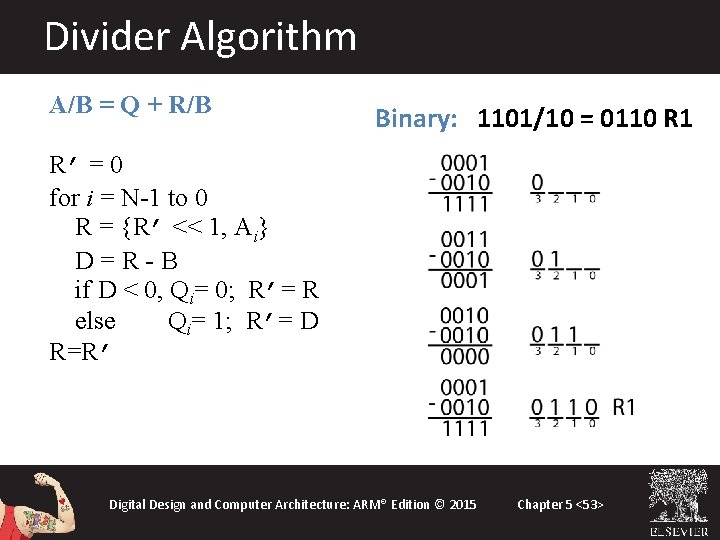
Divider Algorithm A/B = Q + R/B Binary: 1101/10 = 0110 R 1 R’ = 0 for i = N-1 to 0 R = {R’ << 1, Ai} D=R-B if D < 0, Qi= 0; R’= R else Qi= 1; R’= D R=R’ Digital Design and Computer Architecture: ARM® Edition © 2015 Chapter 5 <53>

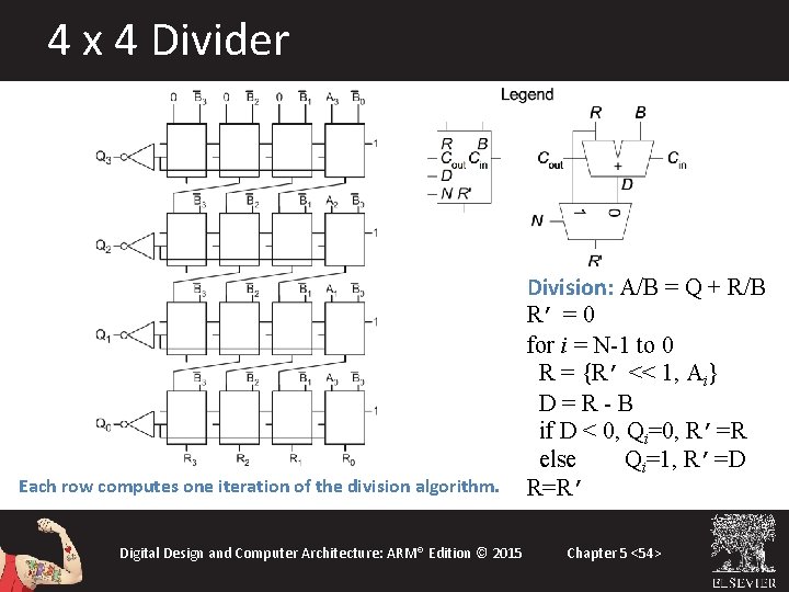
4 x 4 Divider Each row computes one iteration of the division algorithm. Digital Design and Computer Architecture: ARM® Edition © 2015 Division: A/B = Q + R/B R’ = 0 for i = N-1 to 0 R = {R’ << 1, Ai} D=R-B if D < 0, Qi=0, R’=R else Qi=1, R’=D R=R’ Chapter 5 <54>

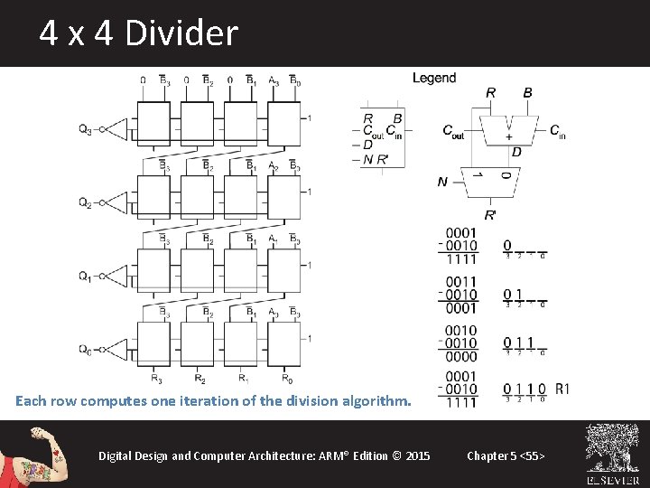
4 x 4 Divider Each row computes one iteration of the division algorithm. Digital Design and Computer Architecture: ARM® Edition © 2015 Chapter 5 <55>

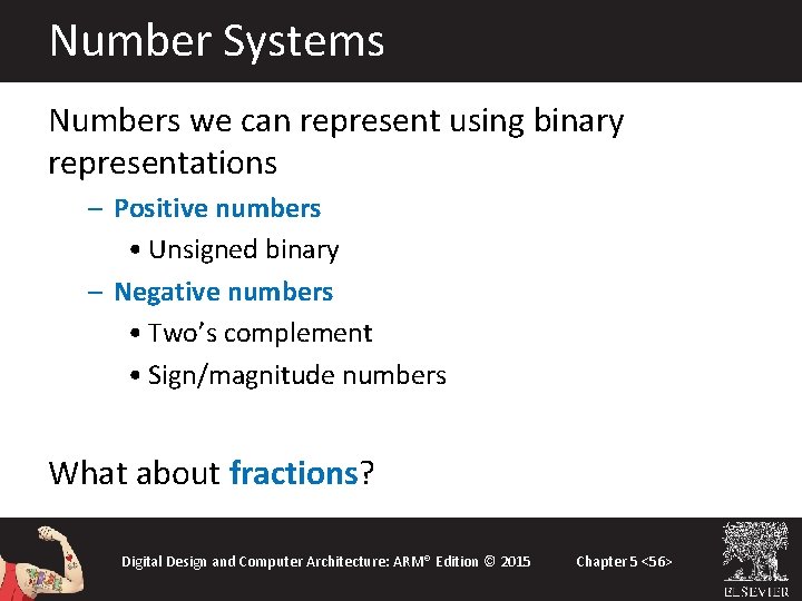
Number Systems Numbers we can represent using binary representations – Positive numbers • Unsigned binary – Negative numbers • Two’s complement • Sign/magnitude numbers What about fractions? Digital Design and Computer Architecture: ARM® Edition © 2015 Chapter 5 <56>

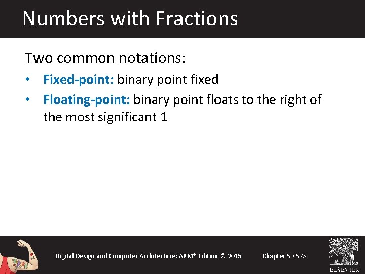
Numbers with Fractions Two common notations: • Fixed-point: binary point fixed • Floating-point: binary point floats to the right of the most significant 1 Digital Design and Computer Architecture: ARM® Edition © 2015 Chapter 5 <57>

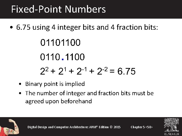
Fixed-Point Numbers • 6. 75 using 4 integer bits and 4 fraction bits: • Binary point is implied • The number of integer and fraction bits must be agreed upon beforehand Digital Design and Computer Architecture: ARM® Edition © 2015 Chapter 5 <58>

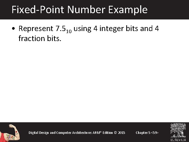
Fixed-Point Number Example • Represent 7. 510 using 4 integer bits and 4 fraction bits. 01111000 Digital Design and Computer Architecture: ARM® Edition © 2015 Chapter 5 <59>

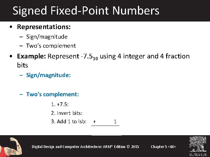
Signed Fixed-Point Numbers • Representations: – Sign/magnitude – Two’s complement • Example: Represent -7. 510 using 4 integer and 4 fraction bits – Sign/magnitude: 11111000 – Two’s complement: 1. +7. 5: 2. Invert bits: 3. Add 1 to lsb: 011110000111 + 1 1000 Digital Design and Computer Architecture: ARM® Edition © 2015 Chapter 5 <60>

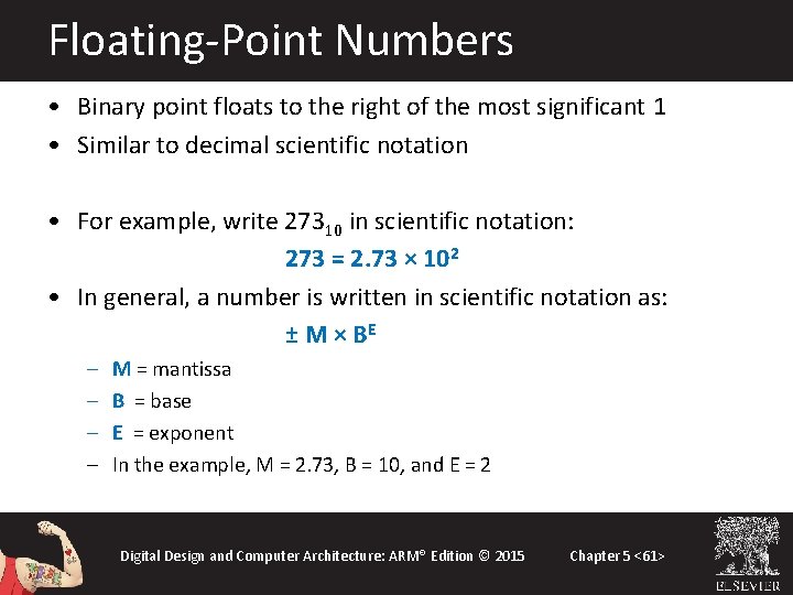
Floating-Point Numbers • Binary point floats to the right of the most significant 1 • Similar to decimal scientific notation • For example, write 27310 in scientific notation: 273 = 2. 73 × 102 • In general, a number is written in scientific notation as: ± M × BE – – M = mantissa B = base E = exponent In the example, M = 2. 73, B = 10, and E = 2 Digital Design and Computer Architecture: ARM® Edition © 2015 Chapter 5 <61>

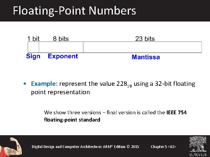
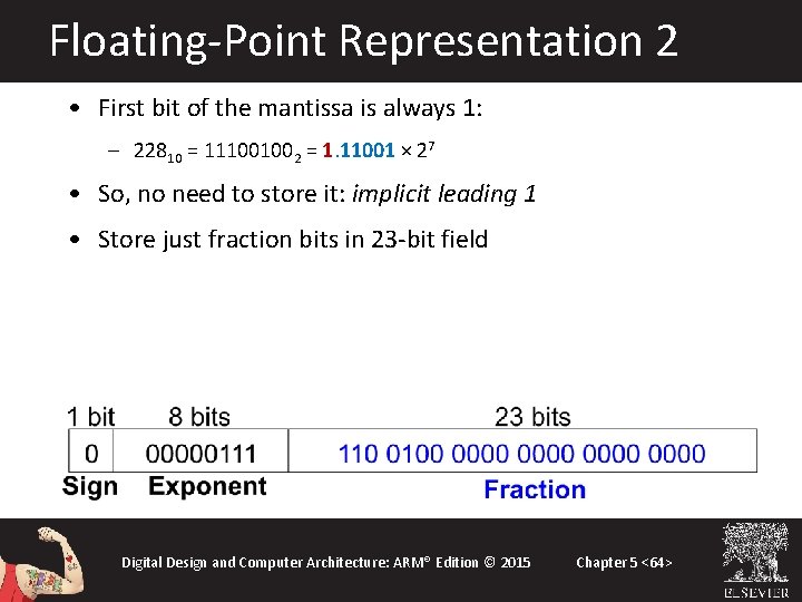
Floating-Point Numbers • Example: represent the value 22810 using a 32 -bit floating point representation We show three versions – final version is called the IEEE 754 floating-point standard Digital Design and Computer Architecture: ARM® Edition © 2015 Chapter 5 <62>

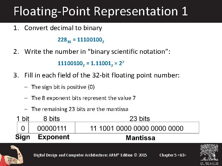
Floating-Point Representation 1 1. Convert decimal to binary 22810 = 111001002 2. Write the number in “binary scientific notation”: 111001002 = 1. 110012 × 27 3. Fill in each field of the 32 -bit floating point number: – The sign bit is positive (0) – The 8 exponent bits represent the value 7 – The remaining 23 bits are the mantissa Digital Design and Computer Architecture: ARM® Edition © 2015 Chapter 5 <63>

Floating-Point Representation 2 • First bit of the mantissa is always 1: – 22810 = 111001002 = 1. 11001 × 27 • So, no need to store it: implicit leading 1 • Store just fraction bits in 23 -bit field Digital Design and Computer Architecture: ARM® Edition © 2015 Chapter 5 <64>

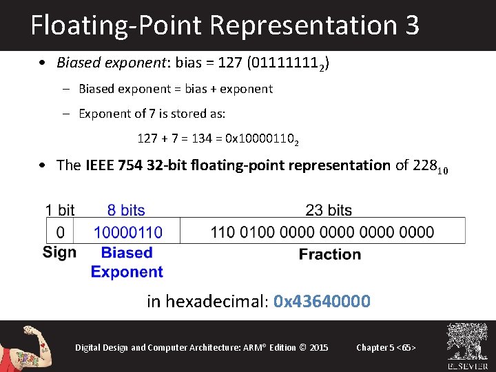
Floating-Point Representation 3 • Biased exponent: bias = 127 (011111112) – Biased exponent = bias + exponent – Exponent of 7 is stored as: 127 + 7 = 134 = 0 x 100001102 • The IEEE 754 32 -bit floating-point representation of 22810 in hexadecimal: 0 x 43640000 Digital Design and Computer Architecture: ARM® Edition © 2015 Chapter 5 <65>

Floating-Point Example Write -58. 2510 in floating point (IEEE 754) Digital Design and Computer Architecture: ARM® Edition © 2015 Chapter 5 <66>

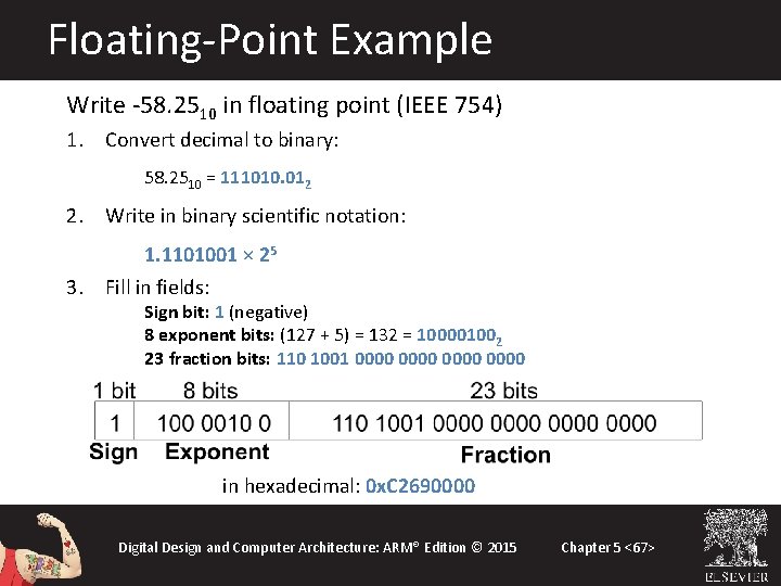
Floating-Point Example Write -58. 2510 in floating point (IEEE 754) 1. Convert decimal to binary: 58. 2510 = 111010. 012 2. Write in binary scientific notation: 3. 1. 1101001 × 25 Fill in fields: Sign bit: 1 (negative) 8 exponent bits: (127 + 5) = 132 = 100001002 23 fraction bits: 110 1001 0000 in hexadecimal: 0 x. C 2690000 Digital Design and Computer Architecture: ARM® Edition © 2015 Chapter 5 <67>

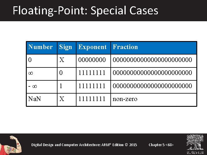
Floating-Point: Special Cases Number Sign Exponent Fraction 0 X 0000000000000000 ∞ 0 1111 000000000000 -∞ 1 1111 000000000000 Na. N X 1111 non-zero Digital Design and Computer Architecture: ARM® Edition © 2015 Chapter 5 <68>

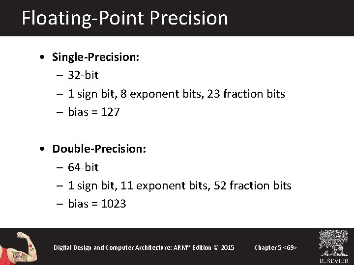
Floating-Point Precision • Single-Precision: – 32 -bit – 1 sign bit, 8 exponent bits, 23 fraction bits – bias = 127 • Double-Precision: – 64 -bit – 1 sign bit, 11 exponent bits, 52 fraction bits – bias = 1023 Digital Design and Computer Architecture: ARM® Edition © 2015 Chapter 5 <69>

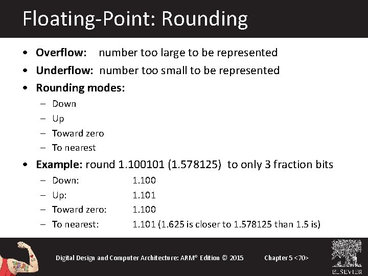
Floating-Point: Rounding • Overflow: number too large to be represented • Underflow: number too small to be represented • Rounding modes: – – Down Up Toward zero To nearest • Example: round 1. 100101 (1. 578125) to only 3 fraction bits – – Down: Up: Toward zero: To nearest: 1. 100 1. 101 (1. 625 is closer to 1. 578125 than 1. 5 is) Digital Design and Computer Architecture: ARM® Edition © 2015 Chapter 5 <70>

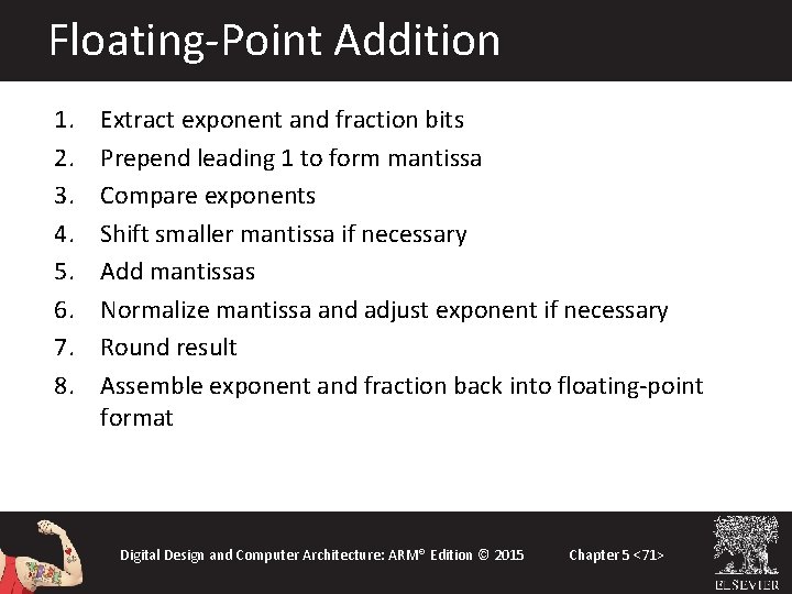
Floating-Point Addition 1. 2. 3. 4. 5. 6. 7. 8. Extract exponent and fraction bits Prepend leading 1 to form mantissa Compare exponents Shift smaller mantissa if necessary Add mantissas Normalize mantissa and adjust exponent if necessary Round result Assemble exponent and fraction back into floating-point format Digital Design and Computer Architecture: ARM® Edition © 2015 Chapter 5 <71>

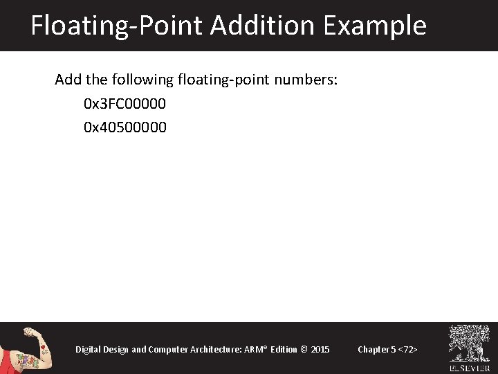
Floating-Point Addition Example Add the following floating-point numbers: 0 x 3 FC 00000 0 x 40500000 Digital Design and Computer Architecture: ARM® Edition © 2015 Chapter 5 <72>

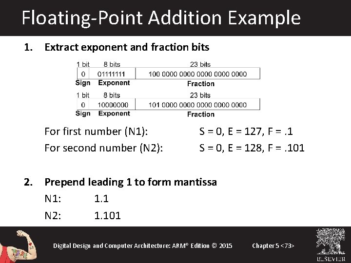
Floating-Point Addition Example 1. Extract exponent and fraction bits For first number (N 1): For second number (N 2): S = 0, E = 127, F =. 1 S = 0, E = 128, F =. 101 2. Prepend leading 1 to form mantissa N 1: 1. 1 N 2: 1. 101 Digital Design and Computer Architecture: ARM® Edition © 2015 Chapter 5 <73>

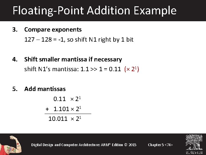
Floating-Point Addition Example 3. Compare exponents 127 – 128 = -1, so shift N 1 right by 1 bit 4. Shift smaller mantissa if necessary shift N 1’s mantissa: 1. 1 >> 1 = 0. 11 (× 21) 5. Add mantissas 0. 11 × 21 + 1. 101 × 21 10. 011 × 21 Digital Design and Computer Architecture: ARM® Edition © 2015 Chapter 5 <74>

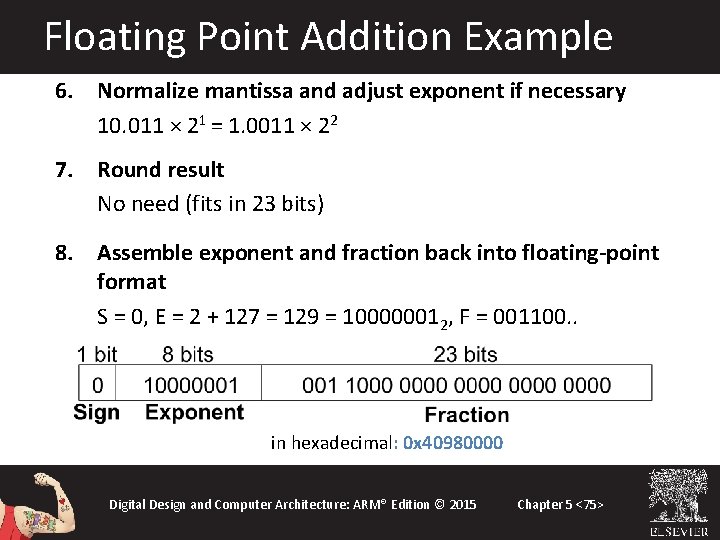
Floating Point Addition Example 6. Normalize mantissa and adjust exponent if necessary 10. 011 × 21 = 1. 0011 × 22 7. Round result No need (fits in 23 bits) 8. Assemble exponent and fraction back into floating-point format S = 0, E = 2 + 127 = 129 = 100000012, F = 001100. . in hexadecimal: 0 x 40980000 Digital Design and Computer Architecture: ARM® Edition © 2015 Chapter 5 <75>

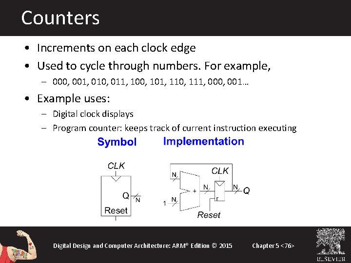
Counters • Increments on each clock edge • Used to cycle through numbers. For example, – 000, 001, 010, 011, 100, 101, 110, 111, 000, 001… • Example uses: – Digital clock displays – Program counter: keeps track of current instruction executing Digital Design and Computer Architecture: ARM® Edition © 2015 Chapter 5 <76>
![Counter Verilog FSM style module counter input logic clk reset output logic N1 0 Counter Verilog (FSM style) module counter (input logic clk, reset, output logic [N-1: 0]](https://slidetodoc.com/presentation_image_h/12c3020cb65ee3a249a5d7ec9fa9271e/image-77.jpg)
Counter Verilog (FSM style) module counter (input logic clk, reset, output logic [N-1: 0] q); logic [N-1: 0] nextq; // register always_ff @(posedge clk, posedge reset) if (reset) q <= 0; else q <= nextq; // next state assign nextq = q + 1; endmodule Digital Design and Computer Architecture: ARM® Edition © 2015 Chapter 5 <77>
![Counter Verilog better idiom module counter input logic clk reset output logic N1 0 Counter Verilog (better idiom) module counter (input logic clk, reset, output logic [N-1: 0]](https://slidetodoc.com/presentation_image_h/12c3020cb65ee3a249a5d7ec9fa9271e/image-78.jpg)
Counter Verilog (better idiom) module counter (input logic clk, reset, output logic [N-1: 0] q); always_ff @(posedge clk, posedge reset) if (reset) q <= 0; else q <= q+1; endmodule Digital Design and Computer Architecture: ARM® Edition © 2015 Chapter 5 <78>

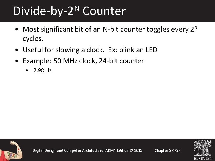
Divide-by-2 N Counter • Most significant bit of an N-bit counter toggles every 2 N cycles. • Useful for slowing a clock. Ex: blink an LED • Example: 50 MHz clock, 24 -bit counter • 2. 98 Hz Digital Design and Computer Architecture: ARM® Edition © 2015 Chapter 5 <79>

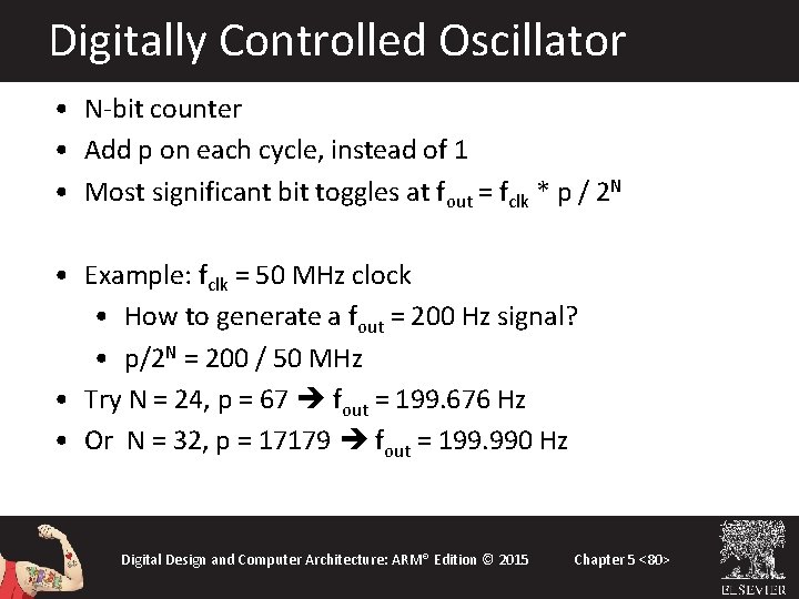
Digitally Controlled Oscillator • N-bit counter • Add p on each cycle, instead of 1 • Most significant bit toggles at fout = fclk * p / 2 N • Example: fclk = 50 MHz clock • How to generate a fout = 200 Hz signal? • p/2 N = 200 / 50 MHz • Try N = 24, p = 67 fout = 199. 676 Hz • Or N = 32, p = 17179 fout = 199. 990 Hz Digital Design and Computer Architecture: ARM® Edition © 2015 Chapter 5 <80>

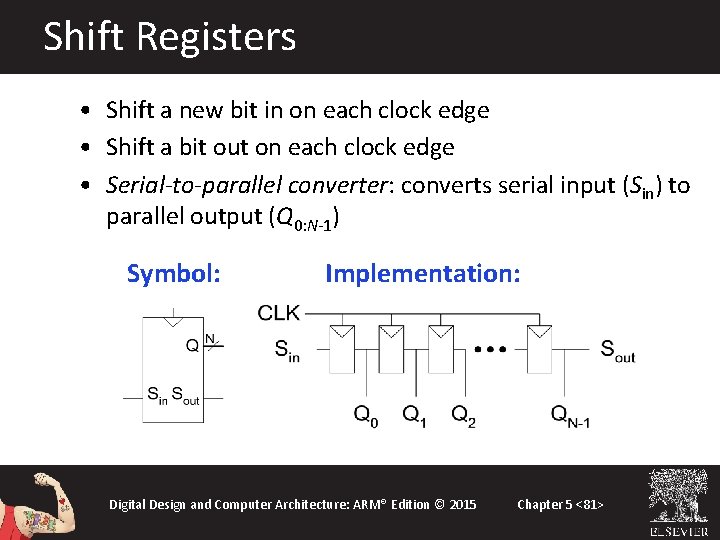
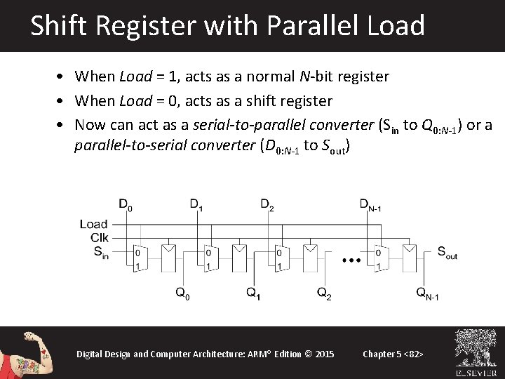
Shift Registers • Shift a new bit in on each clock edge • Shift a bit out on each clock edge • Serial-to-parallel converter: converts serial input (Sin) to parallel output (Q 0: N-1) Symbol: Implementation: Digital Design and Computer Architecture: ARM® Edition © 2015 Chapter 5 <81>

Shift Register with Parallel Load • When Load = 1, acts as a normal N-bit register • When Load = 0, acts as a shift register • Now can act as a serial-to-parallel converter (Sin to Q 0: N-1) or a parallel-to-serial converter (D 0: N-1 to Sout) Digital Design and Computer Architecture: ARM® Edition © 2015 Chapter 5 <82>
![Shift Register Verilog Idiom module shiftreginput logic N1 0 output logic alwaysff posedge clk Shift Register Verilog Idiom module shiftreg(input logic [N-1: 0] output logic always_ff @(posedge clk)](https://slidetodoc.com/presentation_image_h/12c3020cb65ee3a249a5d7ec9fa9271e/image-83.jpg)
Shift Register Verilog Idiom module shiftreg(input logic [N-1: 0] output logic always_ff @(posedge clk) if (load) q <= d; else q <= {q[N-2: 0], sin}; assign sout = q[N-1]; endmodule Digital Design and Computer Architecture: ARM® Edition © 2015 clk, load, sin, d, q, sout); Chapter 5 <83>

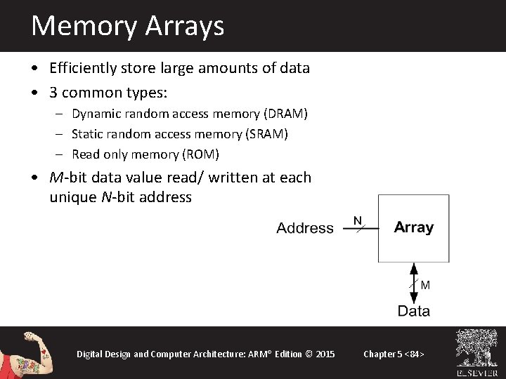
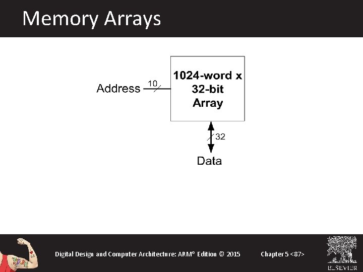
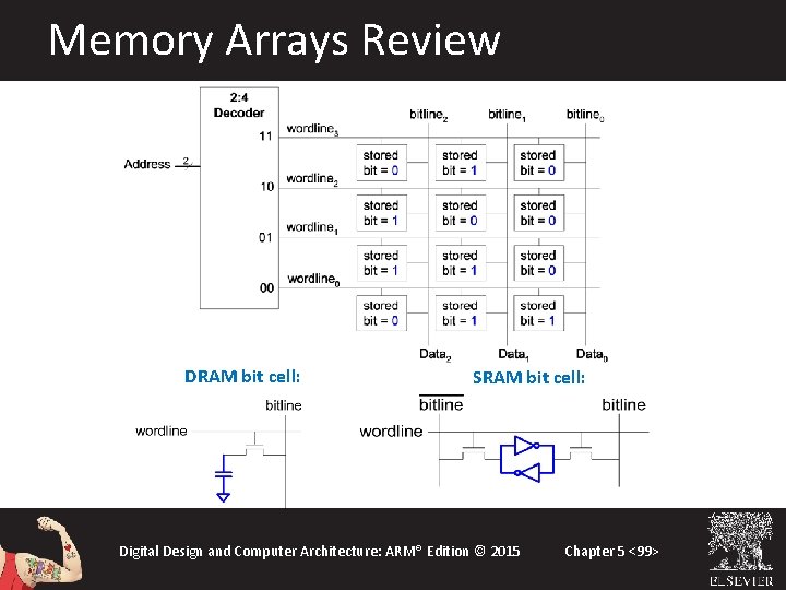
Memory Arrays • Efficiently store large amounts of data • 3 common types: – Dynamic random access memory (DRAM) – Static random access memory (SRAM) – Read only memory (ROM) • M-bit data value read/ written at each unique N-bit address Digital Design and Computer Architecture: ARM® Edition © 2015 Chapter 5 <84>

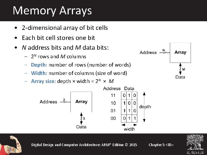
Memory Arrays • 2 -dimensional array of bit cells • Each bit cell stores one bit • N address bits and M data bits: – – 2 N rows and M columns Depth: number of rows (number of words) Width: number of columns (size of word) Array size: depth × width = 2 N × M Digital Design and Computer Architecture: ARM® Edition © 2015 Chapter 5 <85>

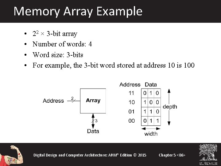
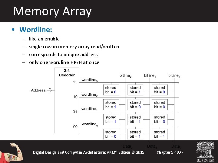
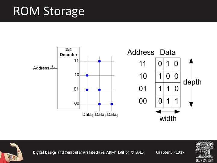
Memory Array Example • • 22 × 3 -bit array Number of words: 4 Word size: 3 -bits For example, the 3 -bit word stored at address 10 is 100 Digital Design and Computer Architecture: ARM® Edition © 2015 Chapter 5 <86>

Memory Arrays Digital Design and Computer Architecture: ARM® Edition © 2015 Chapter 5 <87>

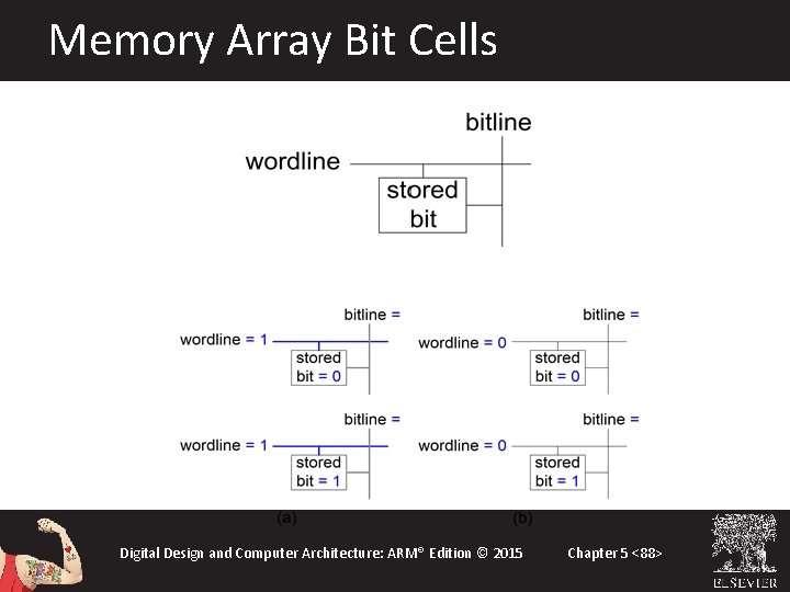
Memory Array Bit Cells Digital Design and Computer Architecture: ARM® Edition © 2015 Chapter 5 <88>

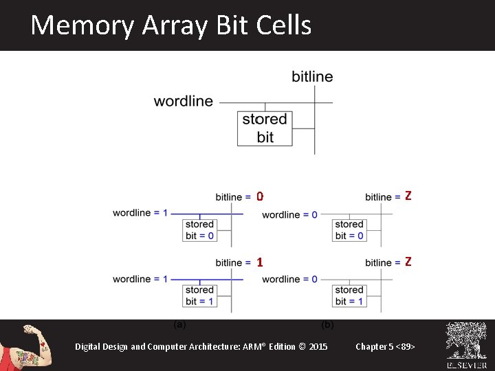
Memory Array Bit Cells 0 Z 1 Z Digital Design and Computer Architecture: ARM® Edition © 2015 Chapter 5 <89>

Memory Array • Wordline: – – like an enable single row in memory array read/written corresponds to unique address only one wordline HIGH at once Digital Design and Computer Architecture: ARM® Edition © 2015 Chapter 5 <90>

Types of Memory • Random access memory (RAM): volatile • Read only memory (ROM): nonvolatile Digital Design and Computer Architecture: ARM® Edition © 2015 Chapter 5 <91>

RAM: Random Access Memory • Volatile: loses its data when power off • Read and written quickly • Main memory in your computer is RAM (DRAM) Historically called random access memory because any data word accessed as easily as any other (in contrast to sequential access memories such as a tape recorder) Digital Design and Computer Architecture: ARM® Edition © 2015 Chapter 5 <92>

ROM: Read Only Memory • Nonvolatile: retains data when power off • Read quickly, but writing is impossible or slow • Flash memory in cameras, thumb drives, and digital cameras are all ROMs Historically called read only memory because ROMs were written at manufacturing time or by burning fuses. Once ROM was configured, it could not be written again. This is no longer the case for Flash memory and other types of ROMs. Digital Design and Computer Architecture: ARM® Edition © 2015 Chapter 5 <93>

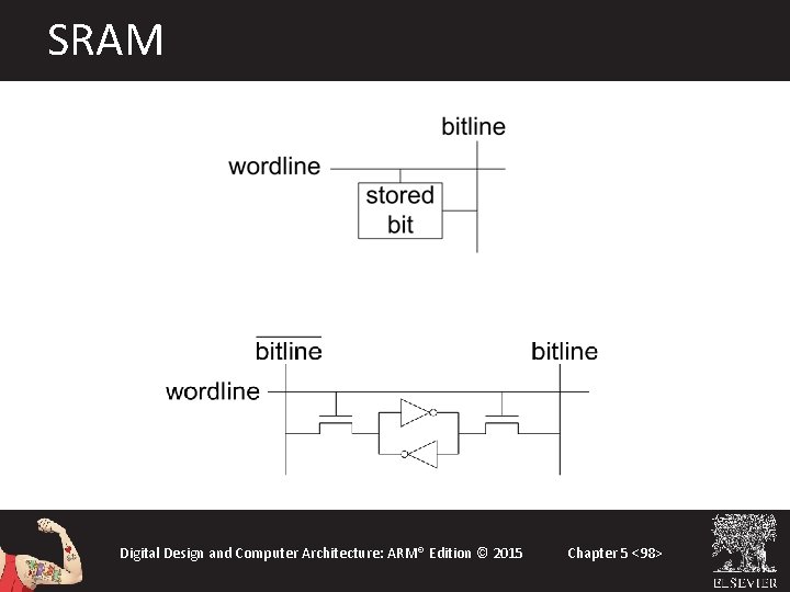
Types of RAM • DRAM (Dynamic random access memory) • SRAM (Static random access memory) • Differ in how they store data: – DRAM uses a capacitor – SRAM uses cross-coupled inverters Digital Design and Computer Architecture: ARM® Edition © 2015 Chapter 5 <94>

Robert Dennard, 1932 • Invented DRAM in 1966 at IBM • Others were skeptical that the idea would work • By the mid-1970’s DRAM in virtually all computers Digital Design and Computer Architecture: ARM® Edition © 2015 Chapter 5 <95>

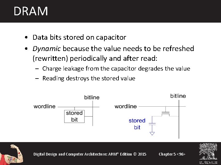
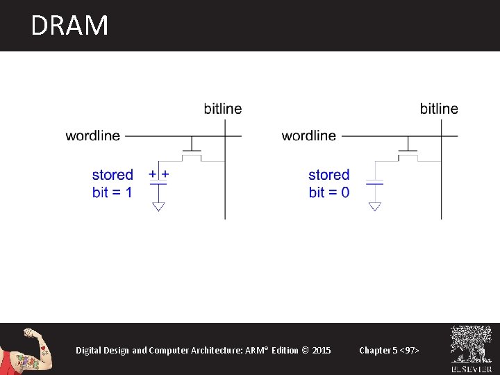
DRAM • Data bits stored on capacitor • Dynamic because the value needs to be refreshed (rewritten) periodically and after read: – Charge leakage from the capacitor degrades the value – Reading destroys the stored value Digital Design and Computer Architecture: ARM® Edition © 2015 Chapter 5 <96>

DRAM Digital Design and Computer Architecture: ARM® Edition © 2015 Chapter 5 <97>

SRAM Digital Design and Computer Architecture: ARM® Edition © 2015 Chapter 5 <98>

Memory Arrays Review DRAM bit cell: SRAM bit cell: Digital Design and Computer Architecture: ARM® Edition © 2015 Chapter 5 <99>

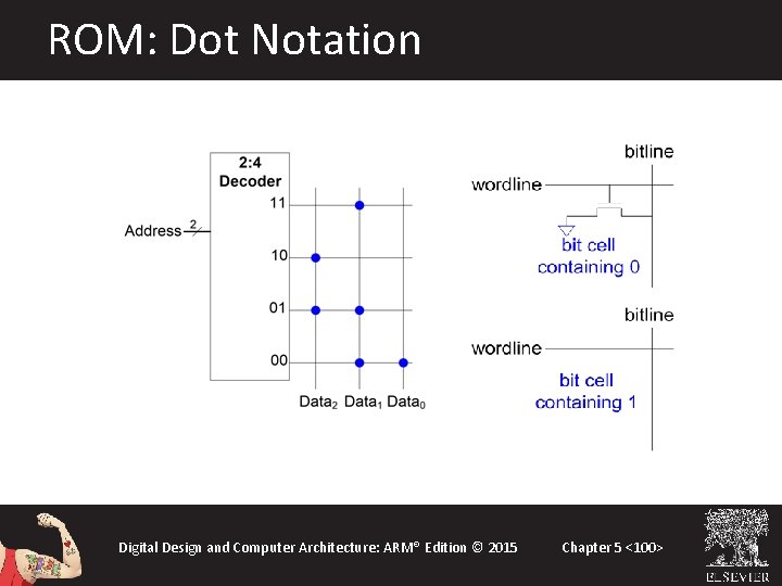
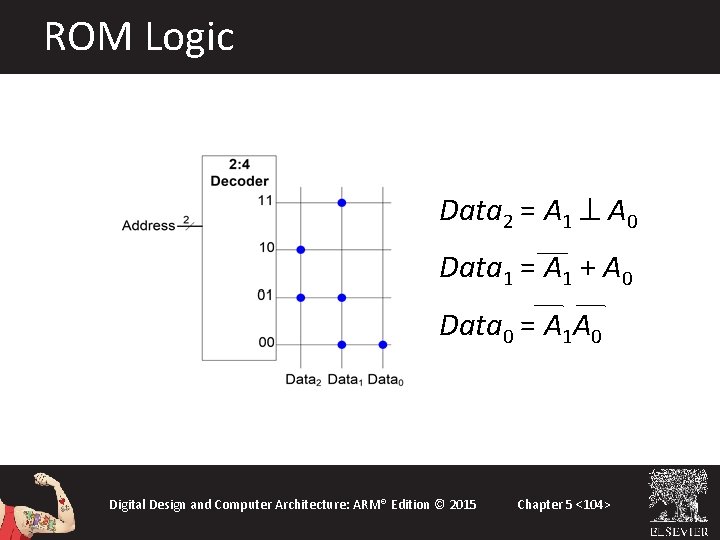
ROM: Dot Notation Digital Design and Computer Architecture: ARM® Edition © 2015 Chapter 5 <100>

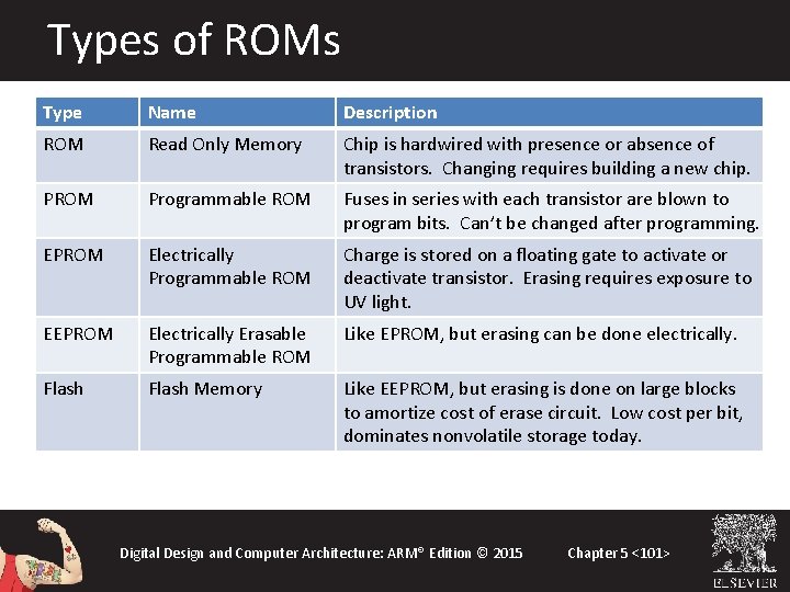
Types of ROMs Type Name Description ROM Read Only Memory Chip is hardwired with presence or absence of transistors. Changing requires building a new chip. PROM Programmable ROM Fuses in series with each transistor are blown to program bits. Can’t be changed after programming. EPROM Electrically Programmable ROM Charge is stored on a floating gate to activate or deactivate transistor. Erasing requires exposure to UV light. EEPROM Electrically Erasable Programmable ROM Like EPROM, but erasing can be done electrically. Flash Memory Like EEPROM, but erasing is done on large blocks to amortize cost of erase circuit. Low cost per bit, dominates nonvolatile storage today. Digital Design and Computer Architecture: ARM® Edition © 2015 Chapter 5 <101>

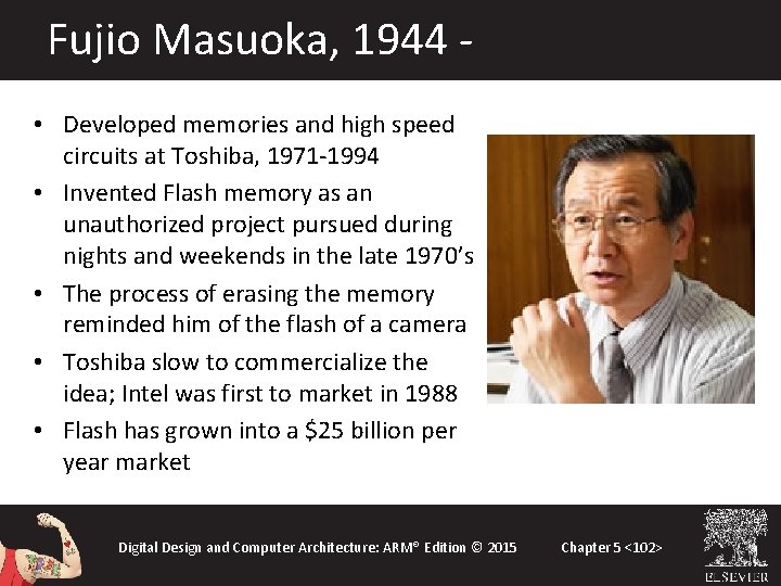
Fujio Masuoka, 1944 • Developed memories and high speed circuits at Toshiba, 1971 -1994 • Invented Flash memory as an unauthorized project pursued during nights and weekends in the late 1970’s • The process of erasing the memory reminded him of the flash of a camera • Toshiba slow to commercialize the idea; Intel was first to market in 1988 • Flash has grown into a $25 billion per year market Digital Design and Computer Architecture: ARM® Edition © 2015 Chapter 5 <102>

ROM Storage Digital Design and Computer Architecture: ARM® Edition © 2015 Chapter 5 <103>

ROM Logic Data 2 = A 1 ^ A 0 Data 1 = A 1 + A 0 Data 0 = A 1 A 0 Digital Design and Computer Architecture: ARM® Edition © 2015 Chapter 5 <104>

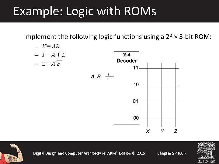
Example: Logic with ROMs Implement the following logic functions using a 22 × 3 -bit ROM: – X = AB – Y=A+B – Z=AB Digital Design and Computer Architecture: ARM® Edition © 2015 Chapter 5 <105>

Example: Logic with ROMs Implement the following logic functions using a 22 × 3 -bit ROM: – X = AB – Y=A+B – Z=AB Digital Design and Computer Architecture: ARM® Edition © 2015 Chapter 5 <106>

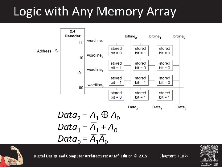
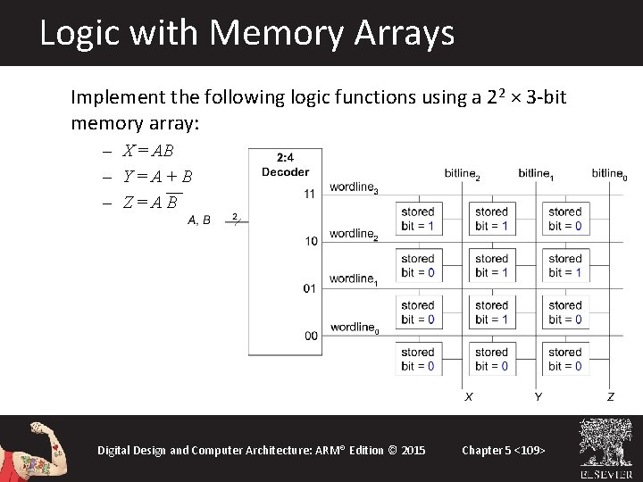
Logic with Any Memory Array Data 2 = A 1 Å A 0 Data 1 = A 1 + A 0 Data 0 = A 1 A 0 Digital Design and Computer Architecture: ARM® Edition © 2015 Chapter 5 <107>

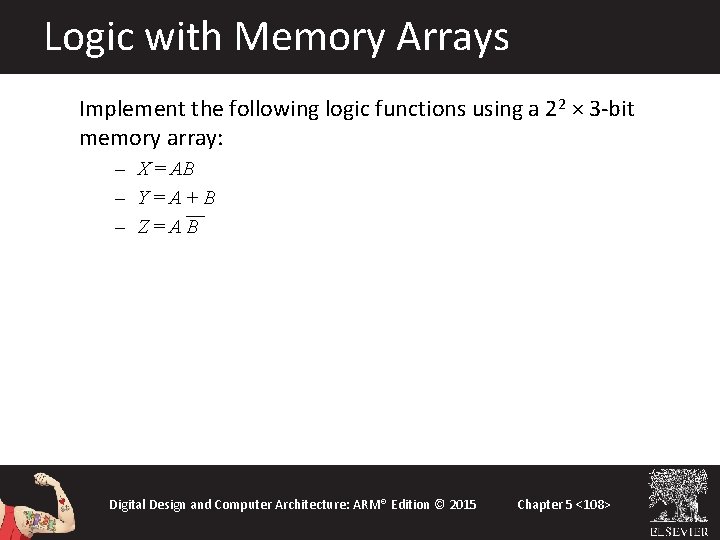
Logic with Memory Arrays Implement the following logic functions using a 22 × 3 -bit memory array: – X = AB – Y=A+B – Z=AB Digital Design and Computer Architecture: ARM® Edition © 2015 Chapter 5 <108>

Logic with Memory Arrays Implement the following logic functions using a 22 × 3 -bit memory array: – X = AB – Y=A+B – Z=AB Digital Design and Computer Architecture: ARM® Edition © 2015 Chapter 5 <109>

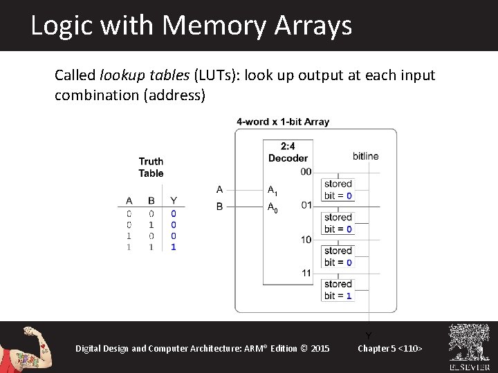
Logic with Memory Arrays Called lookup tables (LUTs): look up output at each input combination (address) Digital Design and Computer Architecture: ARM® Edition © 2015 Chapter 5 <110>

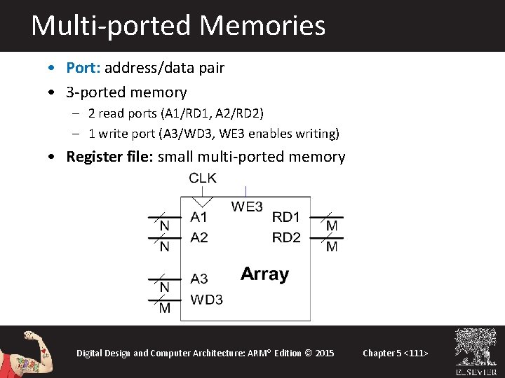
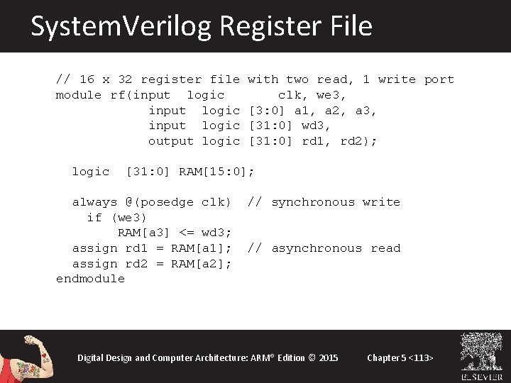
Multi-ported Memories • Port: address/data pair • 3 -ported memory – 2 read ports (A 1/RD 1, A 2/RD 2) – 1 write port (A 3/WD 3, WE 3 enables writing) • Register file: small multi-ported memory Digital Design and Computer Architecture: ARM® Edition © 2015 Chapter 5 <111>

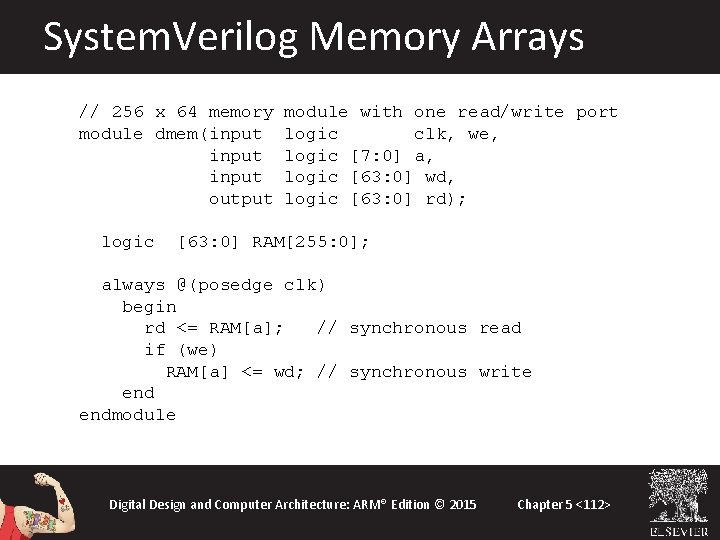
System. Verilog Memory Arrays // 256 x 64 memory module dmem(input output logic module with one read/write port logic clk, we, logic [7: 0] a, logic [63: 0] wd, logic [63: 0] rd); [63: 0] RAM[255: 0]; always @(posedge clk) begin rd <= RAM[a]; // synchronous read if (we) RAM[a] <= wd; // synchronous write endmodule Digital Design and Computer Architecture: ARM® Edition © 2015 Chapter 5 <112>

System. Verilog Register File // 16 x 32 register file module rf(input logic output logic with two read, 1 write port clk, we 3, [3: 0] a 1, a 2, a 3, [31: 0] wd 3, [31: 0] rd 1, rd 2); [31: 0] RAM[15: 0]; always @(posedge clk) if (we 3) RAM[a 3] <= wd 3; assign rd 1 = RAM[a 1]; assign rd 2 = RAM[a 2]; endmodule // synchronous write // asynchronous read Digital Design and Computer Architecture: ARM® Edition © 2015 Chapter 5 <113>

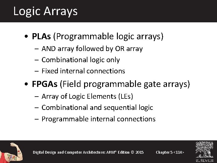
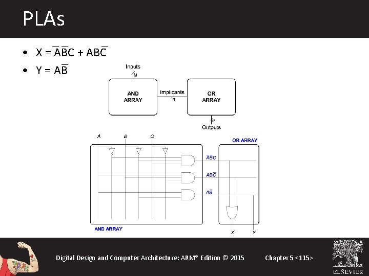
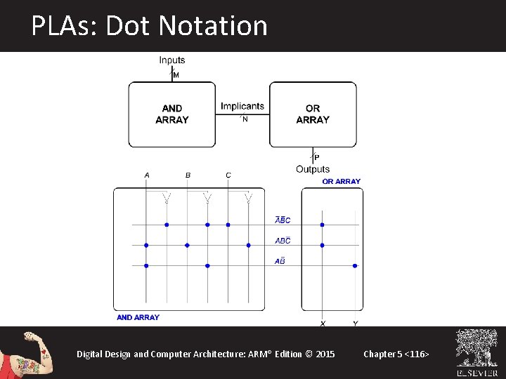
Logic Arrays • PLAs (Programmable logic arrays) – AND array followed by OR array – Combinational logic only – Fixed internal connections • FPGAs (Field programmable gate arrays) – Array of Logic Elements (LEs) – Combinational and sequential logic – Programmable internal connections Digital Design and Computer Architecture: ARM® Edition © 2015 Chapter 5 <114>

PLAs • X = ABC + ABC • Y = AB Digital Design and Computer Architecture: ARM® Edition © 2015 Chapter 5 <115>

PLAs: Dot Notation Digital Design and Computer Architecture: ARM® Edition © 2015 Chapter 5 <116>

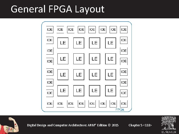
FPGA: Field Programmable Gate Array • Composed of: – LEs (Logic elements): perform logic – IOEs (Input/output elements): interface with outside world – Programmable interconnection: connect LEs and IOEs – Some FPGAs include other building blocks such as multipliers and RAMs Digital Design and Computer Architecture: ARM® Edition © 2015 Chapter 5 <117>

General FPGA Layout Digital Design and Computer Architecture: ARM® Edition © 2015 Chapter 5 <118>

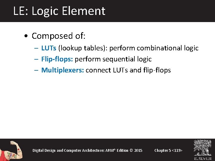
LE: Logic Element • Composed of: – LUTs (lookup tables): perform combinational logic – Flip-flops: perform sequential logic – Multiplexers: connect LUTs and flip-flops Digital Design and Computer Architecture: ARM® Edition © 2015 Chapter 5 <119>

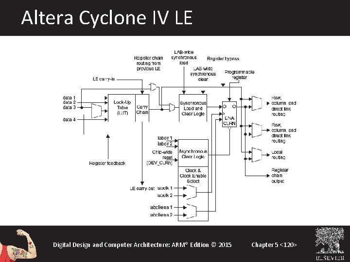
Altera Cyclone IV LE Digital Design and Computer Architecture: ARM® Edition © 2015 Chapter 5 <120>

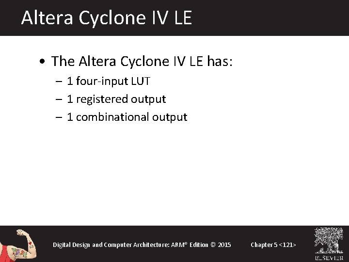
Altera Cyclone IV LE • The Altera Cyclone IV LE has: – 1 four-input LUT – 1 registered output – 1 combinational output Digital Design and Computer Architecture: ARM® Edition © 2015 Chapter 5 <121>

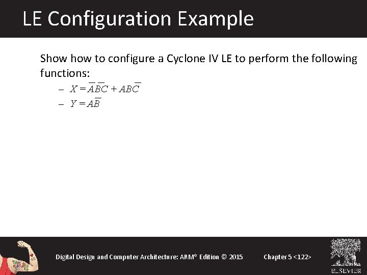
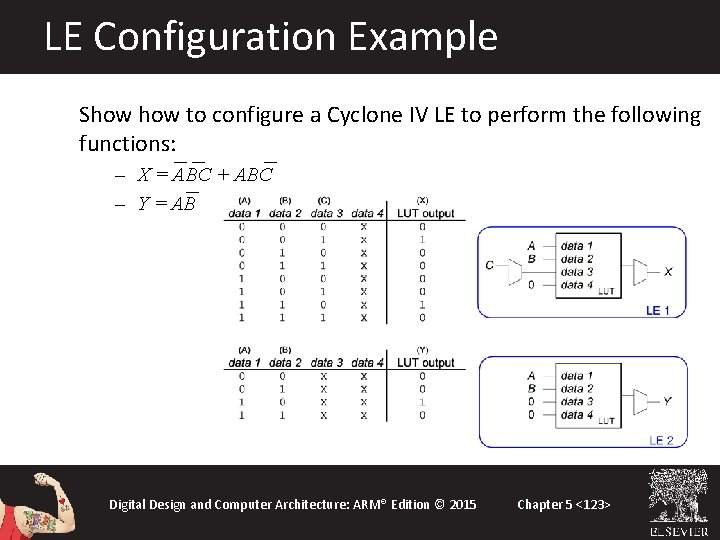
LE Configuration Example Show to configure a Cyclone IV LE to perform the following functions: – X = ABC + ABC – Y = AB Digital Design and Computer Architecture: ARM® Edition © 2015 Chapter 5 <122>

LE Configuration Example Show to configure a Cyclone IV LE to perform the following functions: – X = ABC + ABC – Y = AB Digital Design and Computer Architecture: ARM® Edition © 2015 Chapter 5 <123>

LE Example: AND 5 How many LEs are required to build a 5 -input AND gate? Solution: 2. First performs AND 4 (function of 4 variables). Second performs AND 2 of the first result and the 5 th input. Digital Design and Computer Architecture: ARM® Edition © 2015 Chapter 5 <124>

LE Example: 3 -bit counter How many LEs are required to build a 3 -bit counter? Solution: 3. The counter has 3 flip-flops, so it requires at least 3 LEs. The add logic for each bit is a function of less than 4 variables, so it can fit in the LUT before the flop. Hence, 3 LEs is sufficient. Digital Design and Computer Architecture: ARM® Edition © 2015 Chapter 5 <125>

FPGA Design Flow Using a CAD tool (such as Altera’s Quartus II) • Enter the design with a HDL • Simulate the design • Synthesize design and map it onto FPGA • Download the configuration onto the FPGA • Test the design This is an iterative process! Digital Design and Computer Architecture: ARM® Edition © 2015 Chapter 5 <126>