Chapter 5 Designing Combinational Systems 41 Chapter 5
Chapter 5 Designing Combinational Systems 41
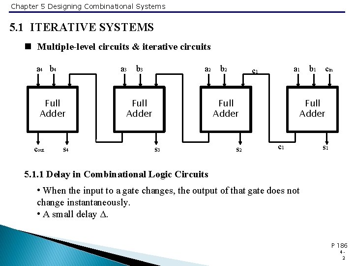
Chapter 5 Designing Combinational Systems 5. 1 ITERATIVE SYSTEMS n Multiple-level circuits & iterative circuits a 4 b 4 a 3 Full Adder cout s 4 b 3 a 2 Full Adder b 2 a 1 c 1 Full Adder s 3 s 2 b 1 cin Full Adder c 1 s 1 5. 1. 1 Delay in Combinational Logic Circuits • When the input to a gate changes, the output of that gate does not change instantaneously. • A small delay Δ. P 186 42
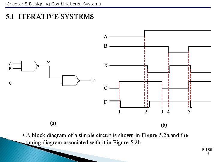
Chapter 5 Designing Combinational Systems 5. 1 ITERATIVE SYSTEMS A B X X F C C F 1 (a) 2 3 4 5 (b) • A block diagram of a simple circuit is shown in Figure 5. 2 a and the timing diagram associated with it in Figure 5. 2 b. P 186 43
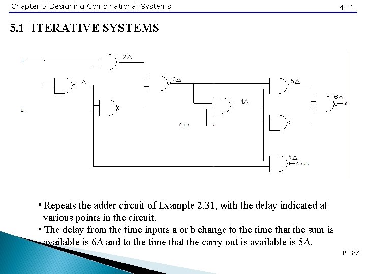
Chapter 5 Designing Combinational Systems 4 -4 5. 1 ITERATIVE SYSTEMS • Repeats the adder circuit of Example 2. 31, with the delay indicated at various points in the circuit. • The delay from the time inputs a or b change to the time that the sum is available is 6Δ and to the time that the carry out is available is 5Δ. P 187
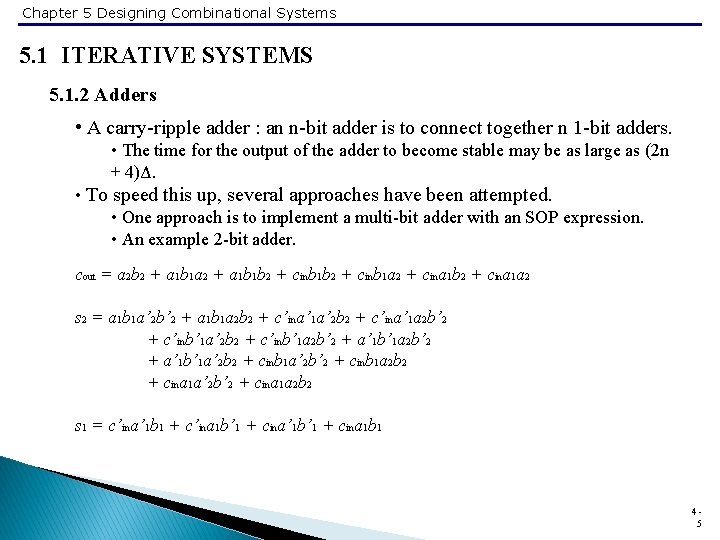
Chapter 5 Designing Combinational Systems 5. 1 ITERATIVE SYSTEMS 5. 1. 2 Adders • A carry-ripple adder : an n-bit adder is to connect together n 1 -bit adders. • The time for the output of the adder to become stable may be as large as (2 n + 4)Δ. • To speed this up, several approaches have been attempted. • One approach is to implement a multi-bit adder with an SOP expression. • An example 2 -bit adder. cout = a 2 b 2 + a 1 b 1 a 2 + a 1 b 1 b 2 + cinb 1 a 2 + cina 1 b 2 + cina 1 a 2 s 2 = a 1 b 1 a’ 2 b’ 2 + a 1 b 1 a 2 b 2 + c’ina’ 1 a’ 2 b 2 + c’ina’ 1 a 2 b’ 2 + c’inb’ 1 a’ 2 b 2 + c’inb’ 1 a 2 b’ 2 + a’ 1 b’ 1 a’ 2 b 2 + cinb 1 a’ 2 b’ 2 + cinb 1 a 2 b 2 + cina 1 a’ 2 b’ 2 + cina 1 a 2 b 2 s 1 = c’ina’ 1 b 1 + c’ina 1 b’ 1 + cina’ 1 b’ 1 + cina 1 b 1 45
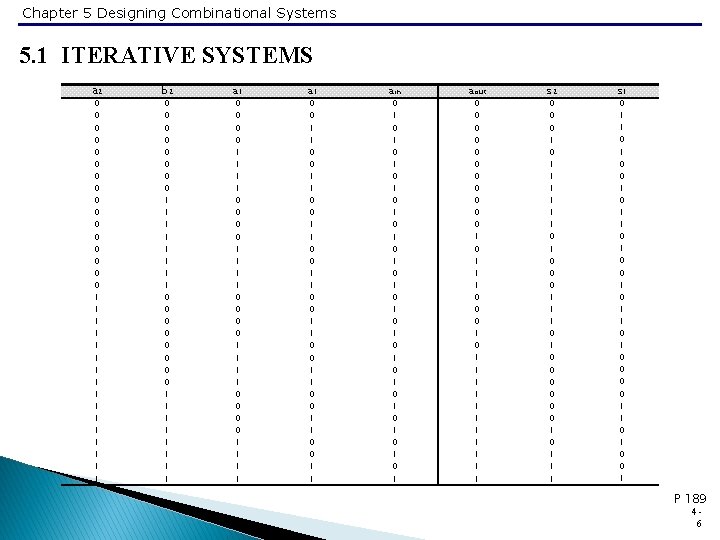
Chapter 5 Designing Combinational Systems 5. 1 ITERATIVE SYSTEMS a 2 b 2 a 1 ain aout s 2 s 1 0 0 1 1 0 0 0 1 1 1 0 0 0 0 1 1 0 0 0 0 1 1 1 1 0 0 0 0 1 1 1 1 0 0 0 1 1 1 1 0 0 0 0 1 1 0 1 1 0 0 1 1 0 0 1 0 1 0 1 0 1 0 0 0 0 0 1 0 1 1 1 0 0 0 1 1 1 0 0 0 1 0 1 1 1 1 0 0 0 1 1 0 P 189 46
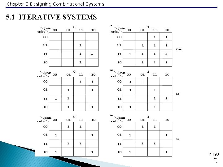
Chapter 5 Designing Combinational Systems 5. 1 ITERATIVE SYSTEMS P 190 47
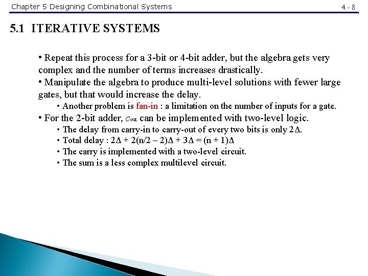
Chapter 5 Designing Combinational Systems 5. 1 ITERATIVE SYSTEMS • Repeat this process for a 3 -bit or 4 -bit adder, but the algebra gets very complex and the number of terms increases drastically. • Manipulate the algebra to produce multi-level solutions with fewer large gates, but that would increase the delay. • Another problem is fan-in : a limitation on the number of inputs for a gate. • For the 2 -bit adder, cout can be implemented with two-level logic. • The delay from carry-in to carry-out of every two bits is only 2Δ. • Total delay : 2Δ + 2(n/2 – 2)Δ + 3Δ = (n + 1)Δ • The carry is implemented with a two-level circuit. • The sum is a less complex multilevel circuit. 4 -8
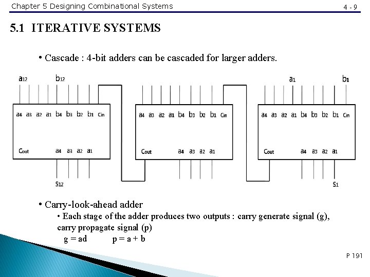
Chapter 5 Designing Combinational Systems 4 -9 5. 1 ITERATIVE SYSTEMS • Cascade : 4 -bit adders can be cascaded for larger adders. • Carry-look-ahead adder • Each stage of the adder produces two outputs : carry generate signal (g), carry propagate signal (p) g = ad p=a+b P 191
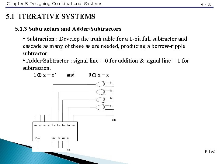
Chapter 5 Designing Combinational Systems 4 - 10 5. 1 ITERATIVE SYSTEMS 5. 1. 3 Subtractors and Adder/Subtractors • Subtraction : Develop the truth table for a 1 -bit full subtractor and cascade as many of these as are needed, producing a borrow-ripple subtractor. • Adder/Subtractor : signal line = 0 for addition & signal line = 1 for subtraction. 1 x = x’ and 0 x=x P 192
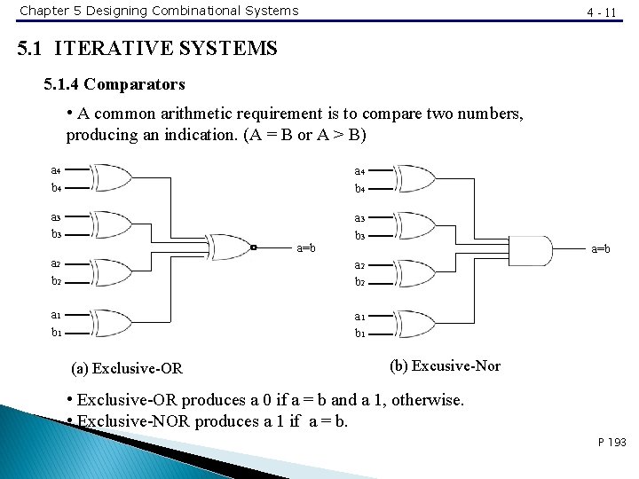
Chapter 5 Designing Combinational Systems 4 - 11 5. 1 ITERATIVE SYSTEMS 5. 1. 4 Comparators • A common arithmetic requirement is to compare two numbers, producing an indication. (A = B or A > B) a 4 b 4 a 3 b 3 a=b a 2 b 2 a 1 b 1 (a) Exclusive-OR a=b (b) Excusive-Nor • Exclusive-OR produces a 0 if a = b and a 1, otherwise. • Exclusive-NOR produces a 1 if a = b. P 193
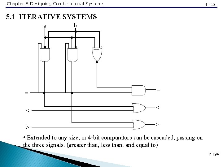
Chapter 5 Designing Combinational Systems 4 - 12 5. 1 ITERATIVE SYSTEMS a = < > b = < > • Extended to any size, or 4 -bit comparators can be cascaded, passing on the three signals. (greater than, less than, and equal to) P 194
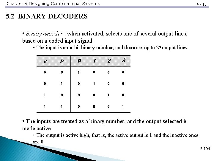
Chapter 5 Designing Combinational Systems 4 - 13 5. 2 BINARY DECODERS • Binary decoder : when activated, selects one of several output lines, based on a coded input signal. • The input is an n-bit binary number, and there are up to 2ⁿ output lines. a b 0 1 2 3 0 0 1 0 0 1 0 0 0 1 • The inputs are treated as a binary number, and the output selected is made active. • The output is active high, that is, the active output is 1 and the inactive ones are 0. P 194
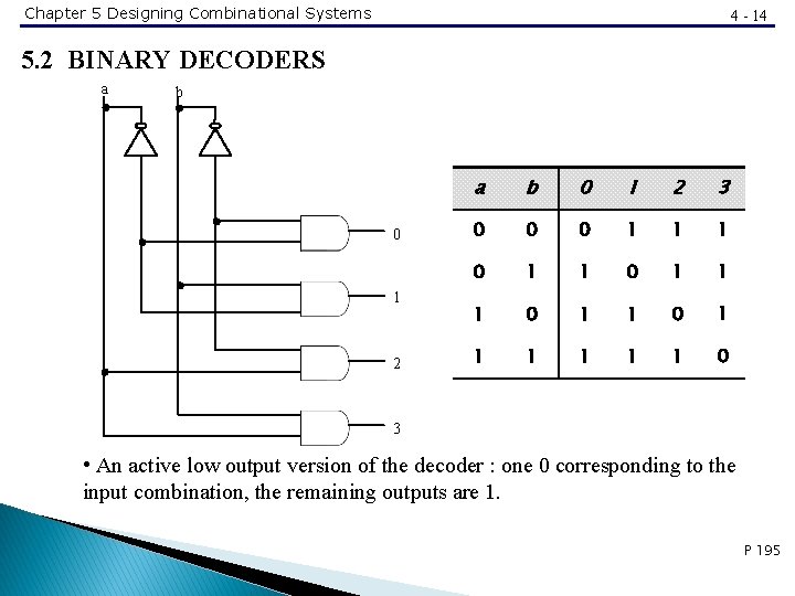
Chapter 5 Designing Combinational Systems 4 - 14 5. 2 BINARY DECODERS a b 0 1 2 3 0 0 0 1 1 1 0 1 1 1 0 3 • An active low output version of the decoder : one 0 corresponding to the input combination, the remaining outputs are 1. P 195
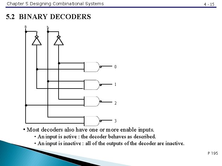
Chapter 5 Designing Combinational Systems 4 - 15 5. 2 BINARY DECODERS a b 0 1 2 3 • Most decoders also have one or more enable inputs. • An input is active : the decoder behaves as described. • An input is inactive : all of the outputs of the decoder are inactive. P 195
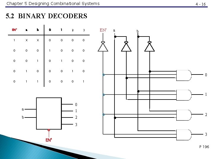
Chapter 5 Designing Combinational Systems 4 - 16 5. 2 BINARY DECODERS EN’ a b 0 1 2 3 1 X X 0 0 0 0 1 0 0 0 1 1 0 0 0 1 EN’ a b 0 1 a 0 1 b 2 2 3 3 EN’ P 196
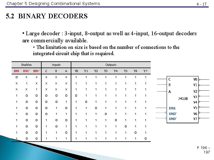
Chapter 5 Designing Combinational Systems 4 - 17 5. 2 BINARY DECODERS • Large decoder : 3 -input, 8 -output as well as 4 -input, 16 -output decoders are commercially available. • The limitation on size is based on the number of connections to the integrated circuit chip that is required. Enables Inputs Outputs EN 1 EN 2’ EN 3’ C B A Y 0 Y 1 Y 2 Y 3 Y 4 Y 5 Y 6 Y 7 0 X X X 1 1 1 1 X 1 X X 1 1 1 1 X X X 1 1 1 1 1 0 0 0 1 1 1 1 0 0 1 1 1 1 0 0 0 1 1 1 0 0 0 1 1 1 1 1 0 0 1 1 1 1 0 1 1 1 0 0 1 1 1 1 0 0 1 1 1 1 1 0 P 196 197
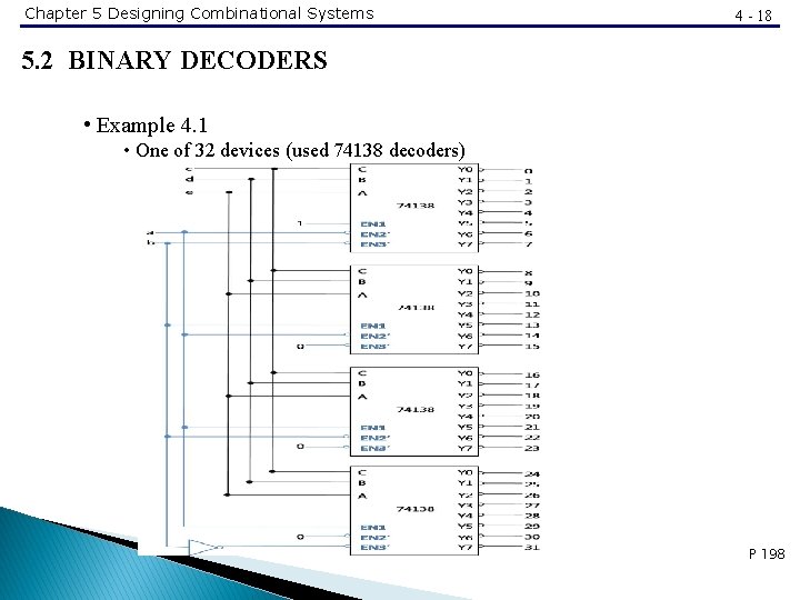
Chapter 5 Designing Combinational Systems 4 - 18 5. 2 BINARY DECODERS • Example 4. 1 • One of 32 devices (used 74138 decoders) P 198
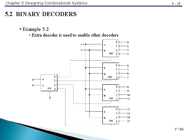
Chapter 5 Designing Combinational Systems 4 - 19 5. 2 BINARY DECODERS • Example 5. 2 • Extra decoder is used to enable other decoders P 199
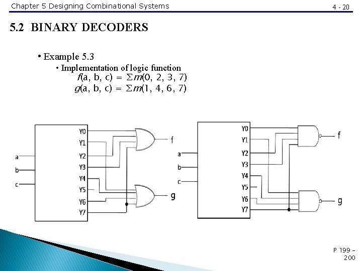
Chapter 5 Designing Combinational Systems 4 - 20 5. 2 BINARY DECODERS • Example 5. 3 • Implementation of logic function f(a, b, c) = ∑m(0, 2, 3, 7) g(a, b, c) = ∑m(1, 4, 6, 7) P 199 200
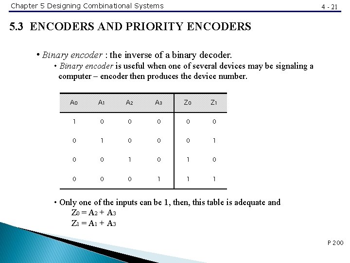
Chapter 5 Designing Combinational Systems 4 - 21 5. 3 ENCODERS AND PRIORITY ENCODERS • Binary encoder : the inverse of a binary decoder. • Binary encoder is useful when one of several devices may be signaling a computer – encoder then produces the device number. A 0 A 1 A 2 A 3 Z 0 Z 1 1 0 0 0 1 0 1 0 0 1 1 1 • Only one of the inputs can be 1, then, this table is adequate and Z 0 = A 2 + A 3 Z 1 = A 1 + A 3 P 200
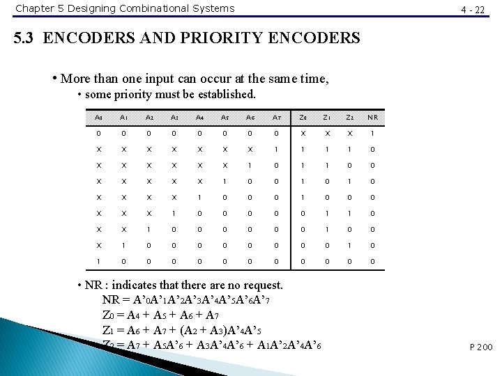
Chapter 5 Designing Combinational Systems 4 - 22 5. 3 ENCODERS AND PRIORITY ENCODERS • More than one input can occur at the same time, • some priority must be established. A 0 A 1 A 2 A 3 A 4 A 5 A 6 A 7 Z 0 Z 1 Z 2 NR 0 0 0 0 X X X 1 X X X X 1 1 0 X X X 1 0 1 1 0 0 X X X 1 0 0 1 0 X X 1 0 0 0 X X X 1 0 0 0 1 1 0 X X 1 0 0 0 1 0 0 X 1 0 0 0 0 0 0 • NR : indicates that there are no request. NR = A’ 0 A’ 1 A’ 2 A’ 3 A’ 4 A’ 5 A’ 6 A’ 7 Z 0 = A 4 + A 5 + A 6 + A 7 Z 1 = A 6 + A 7 + (A 2 + A 3)A’ 4 A’ 5 Z 2 = A 7 + A 5 A’ 6 + A 3 A’ 4 A’ 6 + A 1 A’ 2 A’ 4 A’ 6 P 200
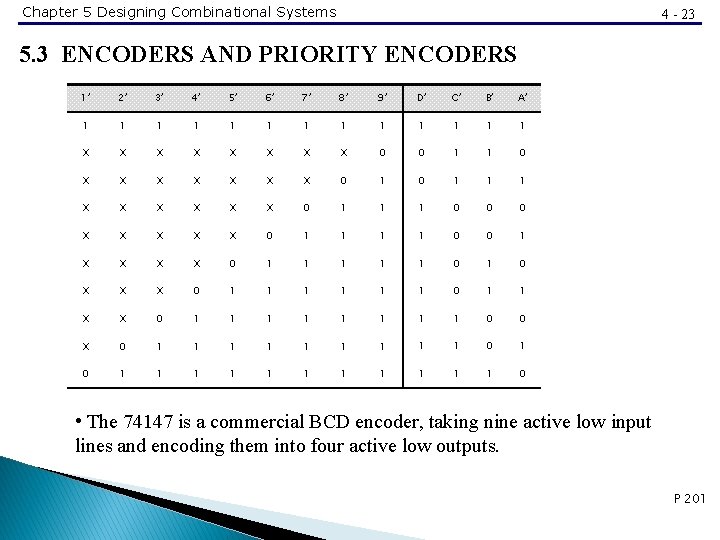
Chapter 5 Designing Combinational Systems 4 - 23 5. 3 ENCODERS AND PRIORITY ENCODERS 1’ 2’ 3’ 4’ 5’ 6’ 7’ 8’ 9’ D’ C’ B’ A’ 1 1 1 1 X X X X 0 0 1 1 0 X X X X 0 1 1 1 0 0 0 X X X 0 1 1 0 0 1 X X 0 1 1 1 0 X X X 0 1 1 1 0 1 1 X X 0 1 1 1 1 0 0 X 0 1 1 1 1 1 1 0 • The 74147 is a commercial BCD encoder, taking nine active low input lines and encoding them into four active low outputs. P 201
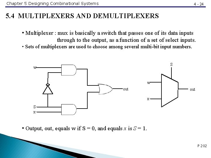
Chapter 5 Designing Combinational Systems 4 - 24 5. 4 MULTIPLEXERS AND DEMULTIPLEXERS • Multiplexer : mux is basically a switch that passes one of its data inputs through to the output, as a function of a set of select inputs. • Sets of multiplexers are used to choose among several multi-bit input numbers. S w w out x S x • Output, out, equals w if S = 0, and equals x is S = 1. P 202
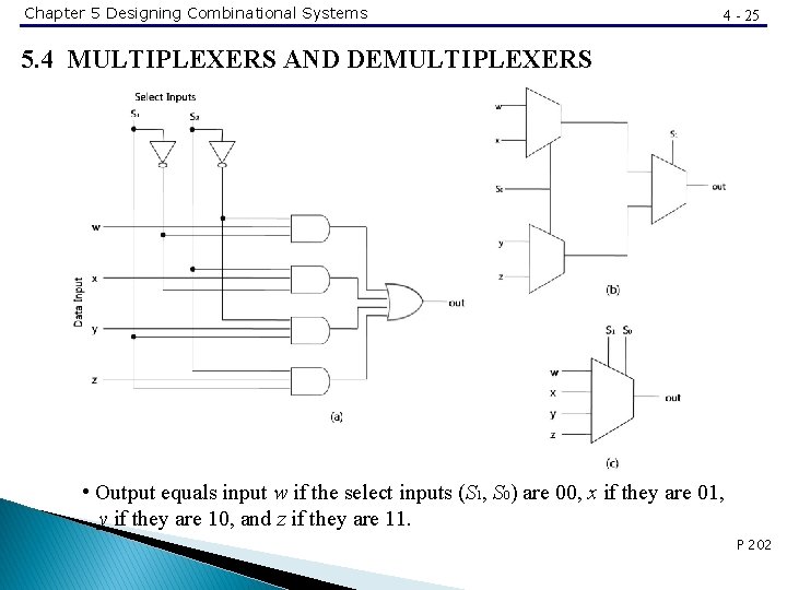
Chapter 5 Designing Combinational Systems 4 - 25 5. 4 MULTIPLEXERS AND DEMULTIPLEXERS • Output equals input w if the select inputs (S 1, S 0) are 00, x if they are 01, y if they are 10, and z if they are 11. P 202
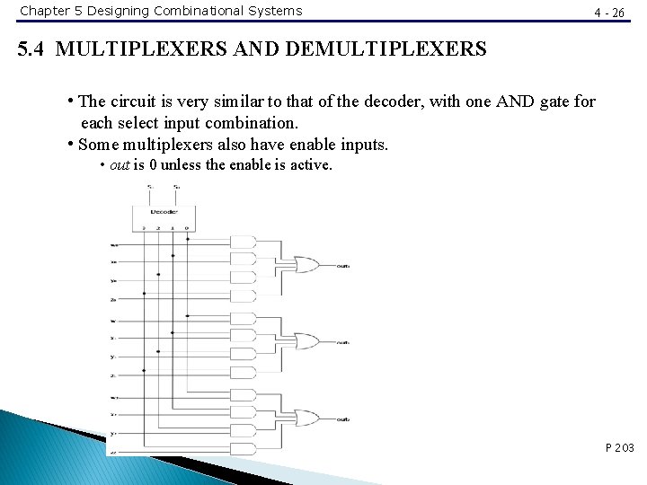
Chapter 5 Designing Combinational Systems 4 - 26 5. 4 MULTIPLEXERS AND DEMULTIPLEXERS • The circuit is very similar to that of the decoder, with one AND gate for each select input combination. • Some multiplexers also have enable inputs. • out is 0 unless the enable is active. P 203
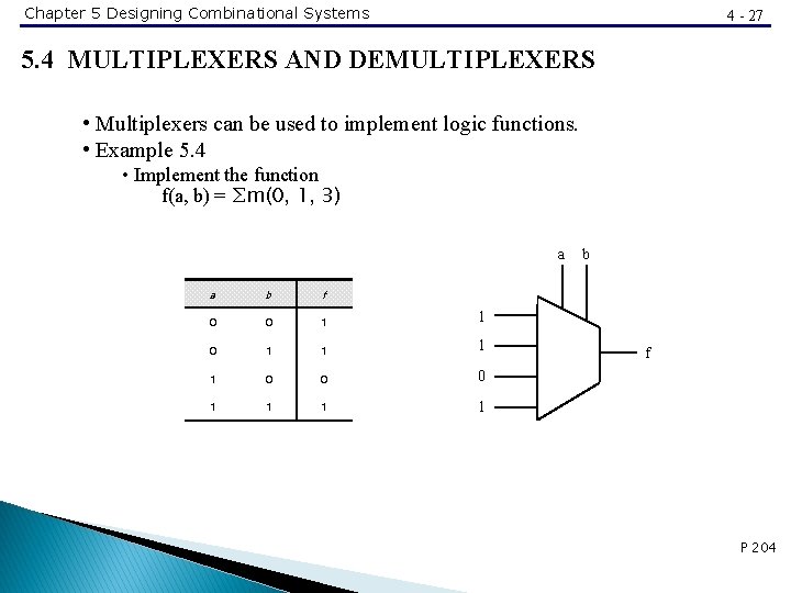
Chapter 5 Designing Combinational Systems 4 - 27 5. 4 MULTIPLEXERS AND DEMULTIPLEXERS • Multiplexers can be used to implement logic functions. • Example 5. 4 • Implement the function f(a, b) = ∑m(0, 1, 3) a a b f 0 0 1 1 1 1 0 0 0 1 1 b f P 204
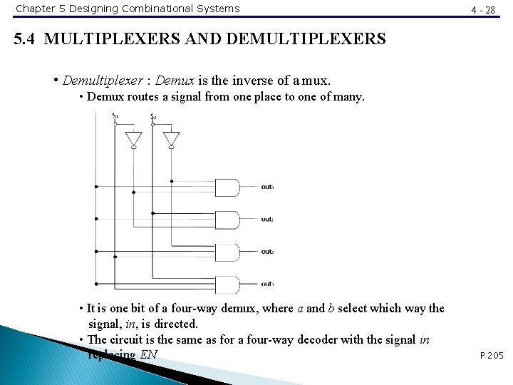
Chapter 5 Designing Combinational Systems 4 - 28 5. 4 MULTIPLEXERS AND DEMULTIPLEXERS • Demultiplexer : Demux is the inverse of a mux. • Demux routes a signal from one place to one of many. • It is one bit of a four-way demux, where a and b select which way the signal, in, is directed. • The circuit is the same as for a four-way decoder with the signal in replacing EN P 205
Chapter 5 Designing Combinational Systems 4 - 29 5. 5 THREE-STATE GATES • Assume that all logic levels were either 0 or 1. And encounter don’t care values. • but in any real circuit implementation, each don’t care took on either the value 0 or 1. • Never connect the output of one gate to the output of another gate, since if the two gates were producing opposite values, there would be a conflict. • Some design techniques have been used that do allow us to connect output to each other. • Three-state output gate. (or tristate output gates) • In a three-state gate, there is an enable input, shown on the side of the gate. • Input is active : the gate behaves as usual. • Control input is inactive : the output behaves as if it is not connected. • Output is typically represented by a Z. P 205
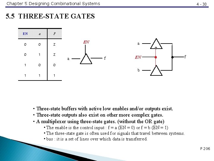
Chapter 5 Designing Combinational Systems 4 - 30 5. 5 THREE-STATE GATES EN a F 0 0 Z 0 1 Z 1 0 0 EN a a f EN f b 1 1 1 • Three-state buffers with active low enables and/or outputs exist. • Three-state outputs also exist on other more complex gates. • A multiplexer using three-state gates. (without the OR gate) • The enable is the control input : f = a (EN = 0) or f = b (EN = 1) • The three-state gate is often used for signals that travel between systems. • bus : it is a set of lines over which data is transferred. P 206
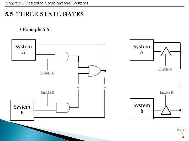
Chapter 5 Designing Combinational Systems 5. 5 THREE-STATE GATES • Example 5. 5 System A Enable A = = = Enable B System B P 206 431
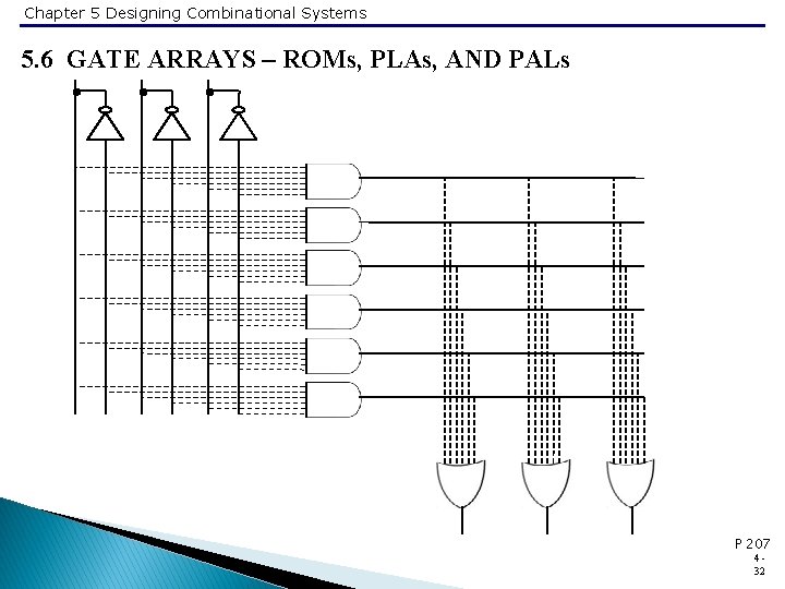
Chapter 5 Designing Combinational Systems 5. 6 GATE ARRAYS – ROMs, PLAs, AND PALs P 207 432
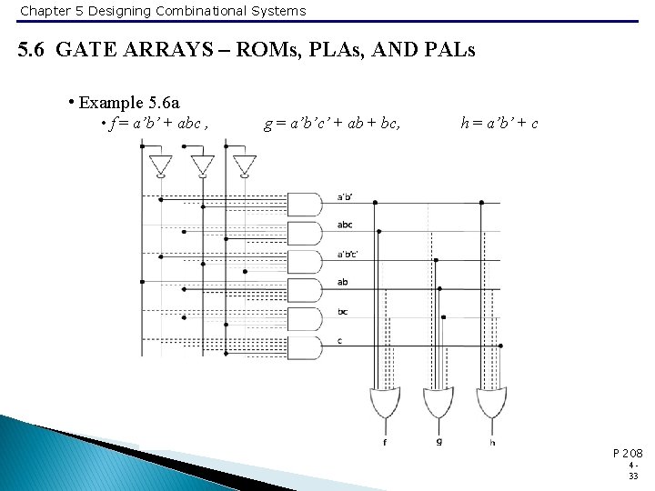
Chapter 5 Designing Combinational Systems 5. 6 GATE ARRAYS – ROMs, PLAs, AND PALs • Example 5. 6 a • f = a’b’ + abc , g = a’b’c’ + ab + bc, h = a’b’ + c P 208 433
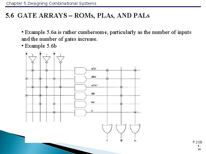
Chapter 5 Designing Combinational Systems 5. 6 GATE ARRAYS – ROMs, PLAs, AND PALs • Example 5. 6 a is rather cumbersome, particularly as the number of inputs and the number of gates increase. • Example 5. 6 b P 209 434
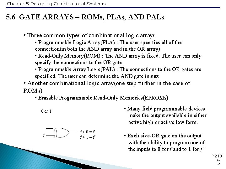
Chapter 5 Designing Combinational Systems 5. 6 GATE ARRAYS – ROMs, PLAs, AND PALs • Three common types of combinational logic arrays • Programmable Logic Array(PLA) : The user specifies all of the connection(in both the AND array and in the OR array) • Read-Only Memory(ROM) : The AND array is fixed. The user can only specify the connections to the OR gate • Programmable Array Logic(PAL) : The connections to the OR gates are specified. The user can determine the AND gate inputs • Another combinational logic array(one step further in the case of ROMs) • Erasable Programmable Read-Only Memories(EPROMs) • Many field programmable devices make the output available in either active high or active low form. 0 or 1 f f+0=f f + 1 = f’ • Exclusive-OR gate on the output with the ability to program one of the inputs to 0 for f and to 1 for f’ P 210 435
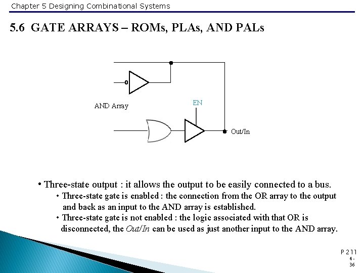
Chapter 5 Designing Combinational Systems 5. 6 GATE ARRAYS – ROMs, PLAs, AND PALs AND Array EN Out/In • Three-state output : it allows the output to be easily connected to a bus. • Three-state gate is enabled : the connection from the OR array to the output and back as an input to the AND array is established. • Three-state gate is not enabled : the logic associated with that OR is disconnected, the Out/In can be used as just another input to the AND array. P 211 436
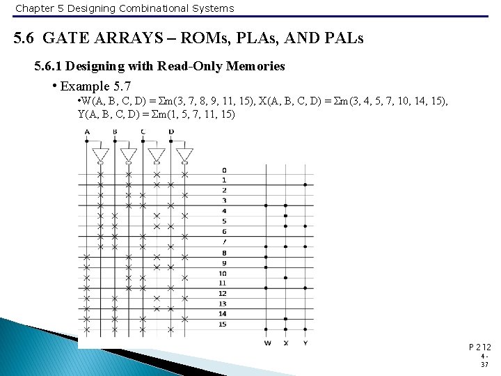
Chapter 5 Designing Combinational Systems 5. 6 GATE ARRAYS – ROMs, PLAs, AND PALs 5. 6. 1 Designing with Read-Only Memories • Example 5. 7 • W(A, B, C, D) = Σm(3, 7, 8, 9, 11, 15), X(A, B, C, D) = Σm(3, 4, 5, 7, 10, 14, 15), Y(A, B, C, D) = Σm(1, 5, 7, 11, 15) P 212 437
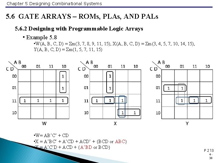
Chapter 5 Designing Combinational Systems 5. 6 GATE ARRAYS – ROMs, PLAs, AND PALs 5. 6. 2 Designing with Programmable Logic Arrays • Example 5. 8 • W(A, B, C, D) = Σm(3, 7, 8, 9, 11, 15), X(A, B, C, D) = Σm(3, 4, 5, 7, 10, 14, 15), Y(A, B, C, D) = Σm(1, 5, 7, 11, 15) • W= AB’C’ + CD • X = A’BC’ + A’CD + ACD’ + {BCD or ABC} • Y = A’C’D + ACD + {A’BD or BCD} P 213 438
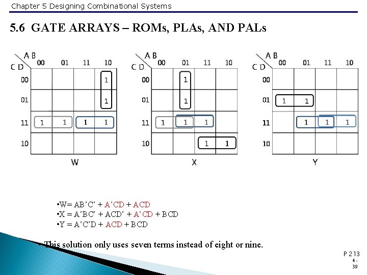
Chapter 5 Designing Combinational Systems 5. 6 GATE ARRAYS – ROMs, PLAs, AND PALs • W= AB’C’ + A’CD + ACD • X = A’BC’ + ACD’ + A’CD + BCD • Y = A’C’D + ACD + BCD • This solution only uses seven terms instead of eight or nine. P 213 439
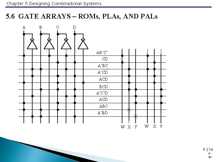
Chapter 5 Designing Combinational Systems 5. 6 GATE ARRAYS – ROMs, PLAs, AND PALs A B C D AB’C’ CD A’BC A’CD’ ACD ’ BCD A’C’D ACD ABC A’BD W X Y P 214 440
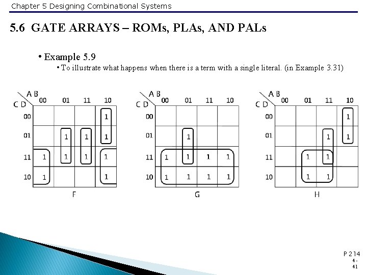
Chapter 5 Designing Combinational Systems 5. 6 GATE ARRAYS – ROMs, PLAs, AND PALs • Example 5. 9 • To illustrate what happens when there is a term with a single literal. (in Example 3. 31) P 214 441

Chapter 5 Designing Combinational Systems 5. 6 GATE ARRAYS – ROMs, PLAs, AND PALs A B C D B’C AB’C ’A’BD ABD BC C F G H P 215 442
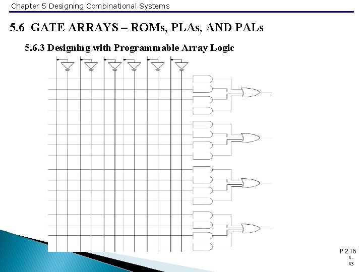
Chapter 5 Designing Combinational Systems 5. 6 GATE ARRAYS – ROMs, PLAs, AND PALs 5. 6. 3 Designing with Programmable Array Logic P 216 443
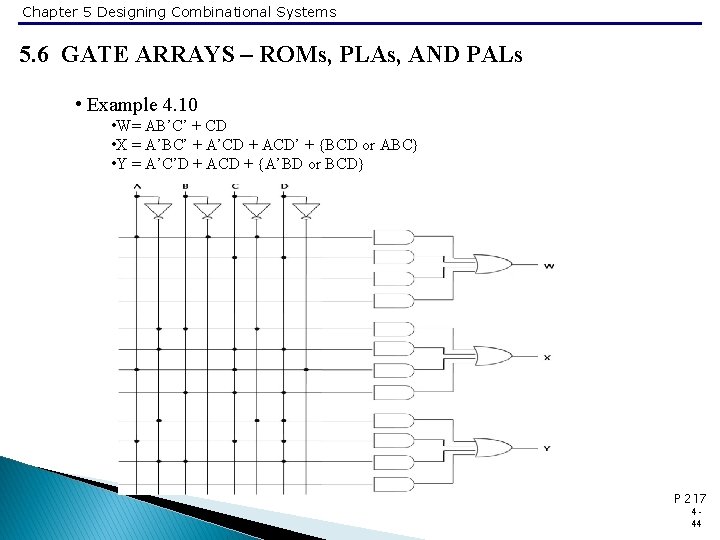
Chapter 5 Designing Combinational Systems 5. 6 GATE ARRAYS – ROMs, PLAs, AND PALs • Example 4. 10 • W= AB’C’ + CD • X = A’BC’ + A’CD + ACD’ + {BCD or ABC} • Y = A’C’D + ACD + {A’BD or BCD} P 217 444
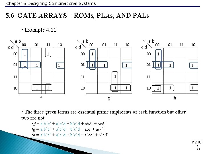
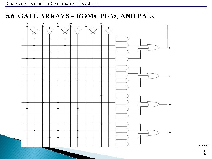
Chapter 5 Designing Combinational Systems 5. 6 GATE ARRAYS – ROMs, PLAs, AND PALs • Example 4. 11 • The three green terms are essential prime implicants of each function but other two are not. • f = a’b’c’ + a’c’d + b’c’d + abd’ + bcd’ • g = a’b’c’ + a’c’d + b’c’d + abc + acd’ • h = a’b’c’ + a’c’d + b’c’d + a’cd’ + b’cd’ P 218 445
Chapter 5 Designing Combinational Systems 5. 6 GATE ARRAYS – ROMs, PLAs, AND PALs P 219 446
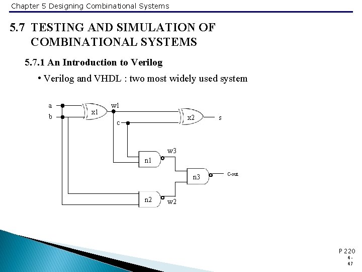
Chapter 5 Designing Combinational Systems 5. 7 TESTING AND SIMULATION OF COMBINATIONAL SYSTEMS 5. 7. 1 An Introduction to Verilog • Verilog and VHDL : two most widely used system a b x 1 w 1 x 2 c s w 3 n 1 n 3 n 2 c-out w 2 P 220 447
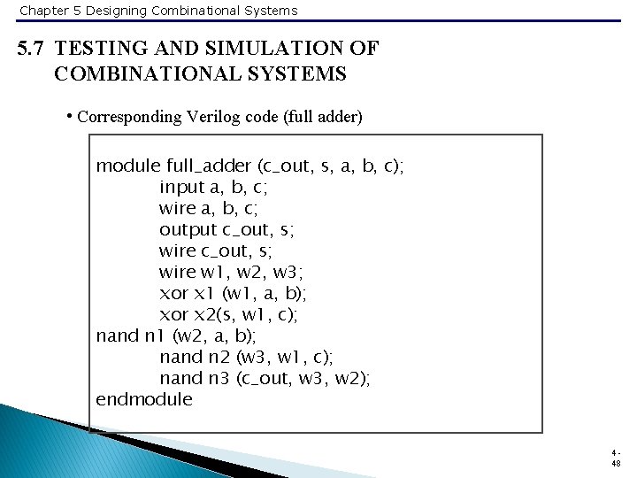
Chapter 5 Designing Combinational Systems 5. 7 TESTING AND SIMULATION OF COMBINATIONAL SYSTEMS • Corresponding Verilog code (full adder) module full_adder (c_out, s, a, b, c); input a, b, c; wire a, b, c; output c_out, s; wire w 1, w 2, w 3; xor x 1 (w 1, a, b); xor x 2(s, w 1, c); nand n 1 (w 2, a, b); nand n 2 (w 3, w 1, c); nand n 3 (c_out, w 3, w 2); endmodule 448
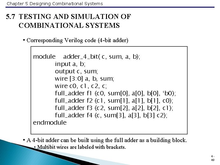
Chapter 5 Designing Combinational Systems 5. 7 TESTING AND SIMULATION OF COMBINATIONAL SYSTEMS • Corresponding Verilog code (4 -bit adder) module adder_4_bit( c, sum, a, b); input a, b; output c, sum; wire [3: 0] a, b, sum; wire c 0, c 1, c 2, c; full_adder f 1 (c 0, sum[0], a[0], b[0], ‘b 0); full_adder f 2 (c 1, sum[1], a[1], b[1], c 0); full_adder f 3 (c 2, sum[2], a[2], b[2], c 1); full_adder f 4 (c, sum[3], a[3], b[3] c 2); endmodule • A 4 -bit adder can be built using the full adder as a building block. • Multibit wires are labeled with brackets. 449
Chapter 5 Designing Combinational Systems 5. 7 TESTING AND SIMULATION OF COMBINATIONAL SYSTEMS • Verilog also providers for the description of the behavior of a system, without specifying the details of the structure. • This is often the first step in the design of a complex system, made up of a number of modules. • The behavioral description of each module can be completed and tested. • Behavioral Verilog uses notation very similar to the C programming language. • The normal mathematics operators are available : +, -, *, / • The bitwise logical operators : ~(not), &(and), |(or), ^(exclusive or) • Two behavioral Verilog descriptions of the full adder. 450
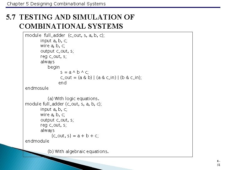
Chapter 5 Designing Combinational Systems 5. 7 TESTING AND SIMULATION OF COMBINATIONAL SYSTEMS module full_adder (c_out, s, a, b, c); input a, b, c; wire a, b, c; output c_out, s; reg c_out, s; always begin s = a ^ b ^ c; c_out = (a & b) | (a & c_in) | (b & c_in); endmosule (a) With logic equations. module full_adder (c_out, s, a, b, c); input a, b, c; wire a, b, c; output c_out, s; reg c_out, s; always {c_out, s} = a + b + c; endmodule (b) With algebraic equations. 451
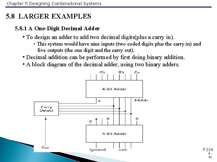
Chapter 5 Designing Combinational Systems 5. 8 LARGER EXAMPLES 5. 8. 1 A One-Digit Decimal Adder • To design an adder to add two decimal digits(plus a carry in). • This system would have nine inputs (two coded digits plus the carry in) and five outputs (the one digit and the carry out). • Decimal addition can be performed by first doing binary addition. • A block diagram of the decimal adder, using two binary adders. P 224 452
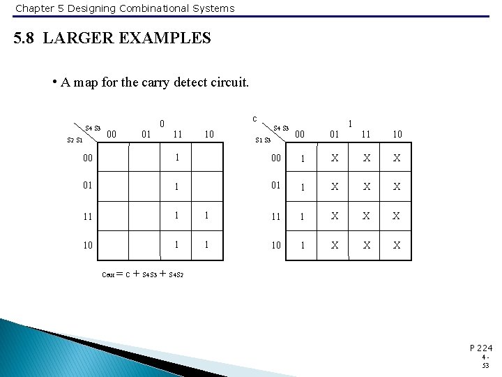
Chapter 5 Designing Combinational Systems 5. 8 LARGER EXAMPLES • A map for the carry detect circuit. s 4 s 3 s 2 s 1 00 01 0 c 11 10 s 4 s 3 s 1 s 3 00 01 1 11 10 00 1 X X X 01 1 X X X 11 1 1 11 1 X X X 10 1 1 10 1 X X X cout = c + s 4 s 3 + s 4 s 2 P 224 453
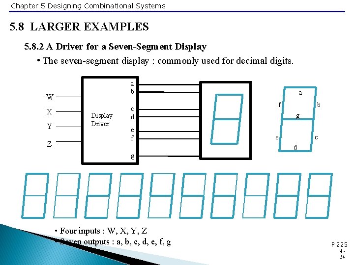
Chapter 5 Designing Combinational Systems 5. 8 LARGER EXAMPLES 5. 8. 2 A Driver for a Seven-Segment Display • The seven-segment display : commonly used for decimal digits. a b W X Y Z Display Driver c d e f a f b g e c d g • Four inputs : W, X, Y, Z • Seven outputs : a, b, c, d, e, f, g P 225 454
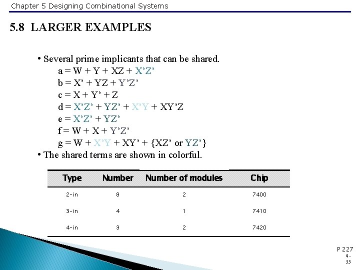
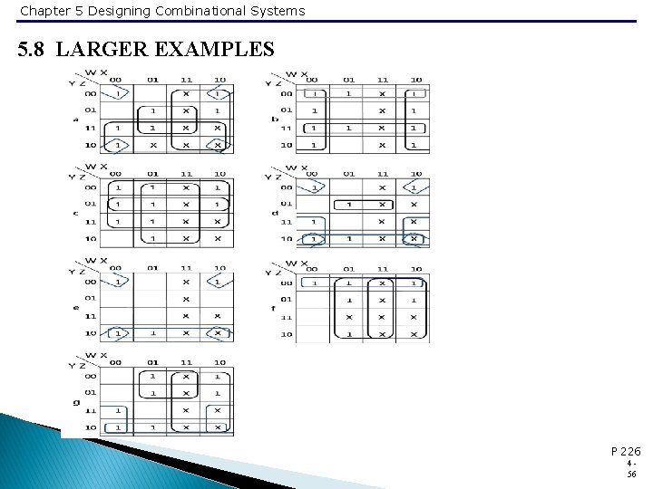
Chapter 5 Designing Combinational Systems 5. 8 LARGER EXAMPLES • Several prime implicants that can be shared. a = W + Y + XZ + X’Z’ b = X’ + YZ + Y’Z’ c = X + Y’ + Z d = X’Z’ + YZ’ + X’Y + XY’Z e = X’Z’ + YZ’ f = W + X + Y’Z’ g = W + X’Y + XY’ + {XZ’ or YZ’} • The shared terms are shown in colorful. Type Number of modules Chip 2 -in 8 2 7400 3 -in 4 1 7410 4 -in 3 2 7420 P 227 455
Chapter 5 Designing Combinational Systems 5. 8 LARGER EXAMPLES P 226 456
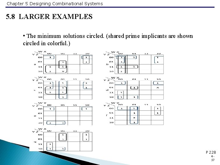
Chapter 5 Designing Combinational Systems 5. 8 LARGER EXAMPLES • The minimum solutions circled. (shared prime implicants are shown circled in colorful. ) P 228 457
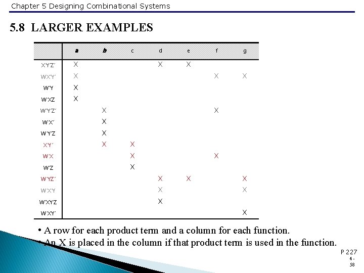
Chapter 5 Designing Combinational Systems 5. 8 LARGER EXAMPLES a X’Y’Z’ X WX’Y’ X W’Y X W’XZ X b W’Y’Z’ X W’X’ X W’Y’Z X X’Y’ X c d e X X g X X W’X X W’Z X X W’YZ’ X W’X’Y X W’XY’Z X W’XY’ f X X • A row for each product term and a column for each function. • An X is placed in the column if that product term is used in the function. P 227 458
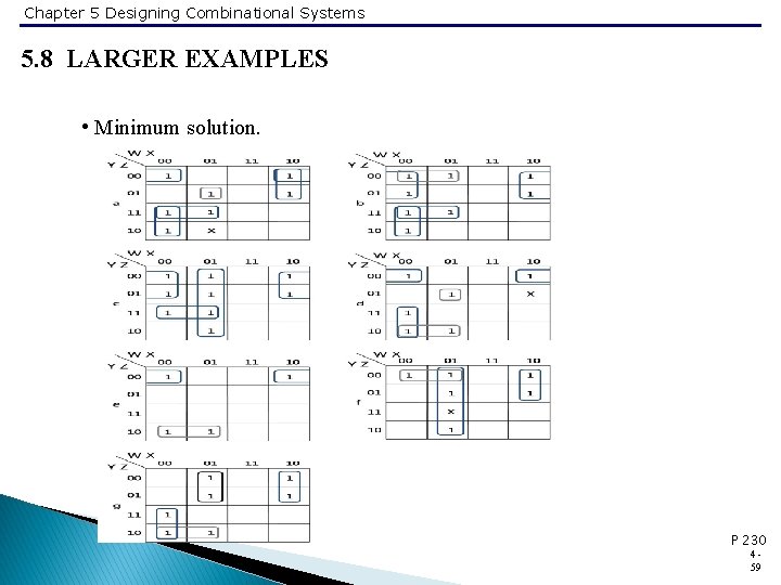
Chapter 5 Designing Combinational Systems 5. 8 LARGER EXAMPLES • Minimum solution. P 230 459
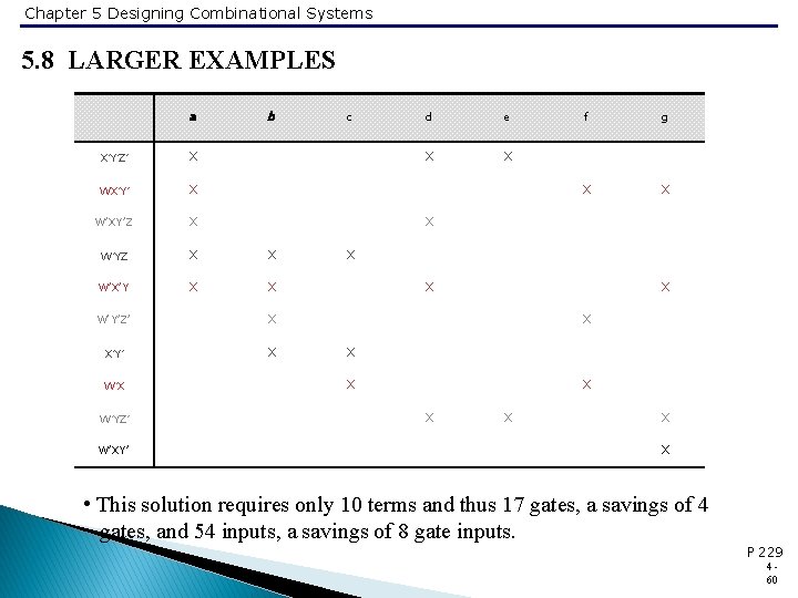
Chapter 5 Designing Combinational Systems 5. 8 LARGER EXAMPLES a b X’Y’Z’ X WX’Y’ X W’XY’Z X W’YZ X X W’X’Y X X’Y’ X W’YZ’ W’XY’ d e X X f g X X X W’Y’Z’ W’X c X X X • This solution requires only 10 terms and thus 17 gates, a savings of 4 gates, and 54 inputs, a savings of 8 gate inputs. P 229 460
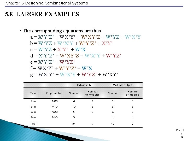
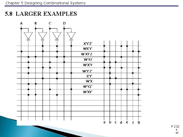
Chapter 5 Designing Combinational Systems 5. 8 LARGER EXAMPLES • The corresponding equations are thus a = X’Y’Z’ + WX’Y’ + W’XY’Z + W’YZ + W’X’Y b = W’YZ + W’X’Y + W’Y’Z’ + X’Y’ c = W’YZ + X’Y’ + W’X d = X’Y’Z’ + W’XY’Z + W’X’Y + W’YZ’ e = X’Y’Z’ + W’YZ’ f = WX’Y’ + W’Y’Z’ + W’X g = WX’Y’ + W’X’Y + W’YZ’ + W’XY’ Individually Multiple output Type Chip number Number of modules Number of module 2 -in 7400 6 2 3 1 3 -in 7410 10 3 9 3 4 -in 7420 5 3 4 2 8 -in 7430 0 1 1 17 7 Total 21 8 P 231 461
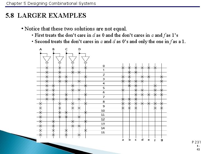
Chapter 5 Designing Combinational Systems 5. 8 LARGER EXAMPLES • Notice that these two solutions are not equal. • First treats the don’t care in d as 0 and the don’t cares in a and f as 1’s • Second treats the don’t cares in a and d as 0’s and only the one in f as a 1. P 231 462
Chapter 5 Designing Combinational Systems 5. 8 LARGER EXAMPLES P 232 463
- Slides: 63