Chapter 5 Computer Organization BrooksCole 2003 OBJECTIVES After
Chapter 5 Computer Organization ©Brooks/Cole, 2003
OBJECTIVES After reading this chapter, the reader should be able to: Distinguish between the three components of a computer hardware. List the functionality of each component. Understand memory addressing and calculate the number of bytes for a specified purpose. Distinguish between different types of memories. Understand how each input/output device works. Continued on the next slide ©Brooks/Cole, 2003
OBJECTIVES (continued) Understand the systems used to connect different components together. Understand the addressing system for input/output devices. Understand the program execution and machine cycles. Distinguish between programmed I/O, interrupt-driven I/O and direct memory access (DMA). Understand the two major architectures used to define the instruction sets of a computer: CISC and RISC. ©Brooks/Cole, 2003
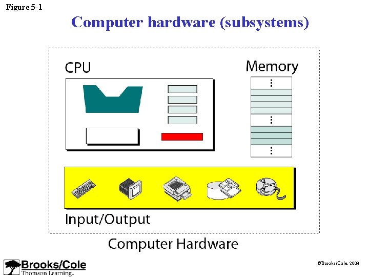
Figure 5 -1 Computer hardware (subsystems) ©Brooks/Cole, 2003
5. 1 CENTRAL PROCESSING UNIT (CPU) ©Brooks/Cole, 2003
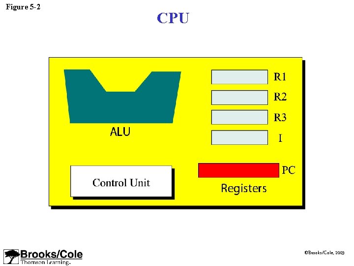
Figure 5 -2 CPU ©Brooks/Cole, 2003
5. 2 MAIN MEMORY ©Brooks/Cole, 2003
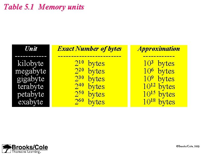
Table 5. 1 Memory units Unit ------kilobyte megabyte gigabyte terabyte petabyte exabyte Exact Number of bytes ------------210 bytes 220 bytes 230 bytes 240 bytes 250 bytes 260 bytes Approximation ------103 bytes 106 bytes 109 bytes 1012 bytes 1015 bytes 1018 bytes ©Brooks/Cole, 2003
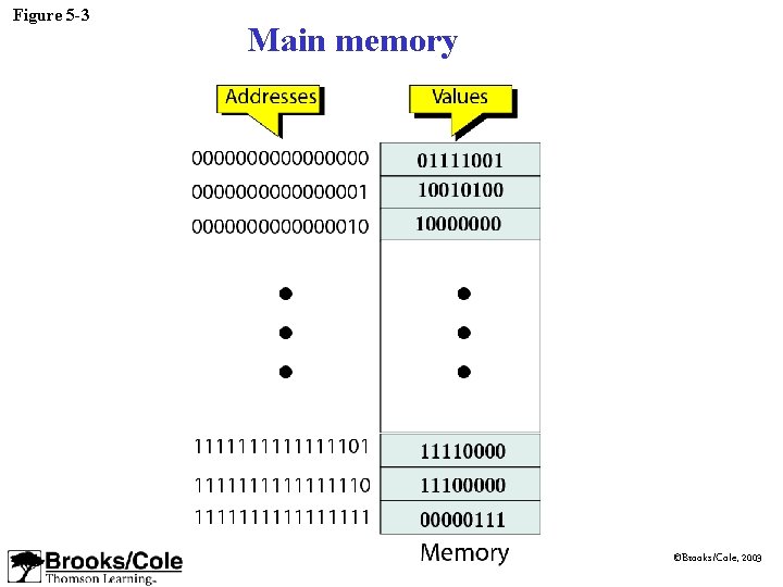
Figure 5 -3 Main memory ©Brooks/Cole, 2003
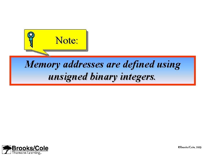
Note: Memory addresses are defined using unsigned binary integers. ©Brooks/Cole, 2003
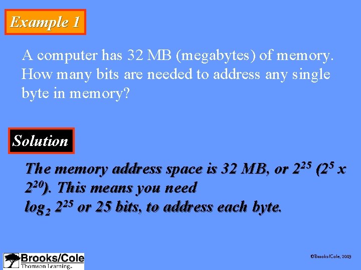
Example 1 A computer has 32 MB (megabytes) of memory. How many bits are needed to address any single byte in memory? Solution The memory address space is 32 MB, or 225 (25 x 220). This means you need log 2 225 or 25 bits, to address each byte. ©Brooks/Cole, 2003
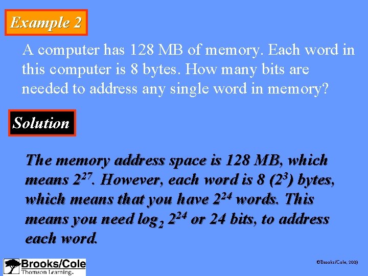
Example 2 A computer has 128 MB of memory. Each word in this computer is 8 bytes. How many bits are needed to address any single word in memory? Solution The memory address space is 128 MB, which means 227. However, each word is 8 (23) bytes, which means that you have 224 words. This means you need log 2 224 or 24 bits, to address each word. ©Brooks/Cole, 2003
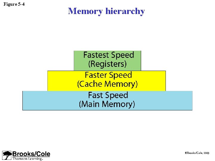
Figure 5 -4 Memory hierarchy ©Brooks/Cole, 2003
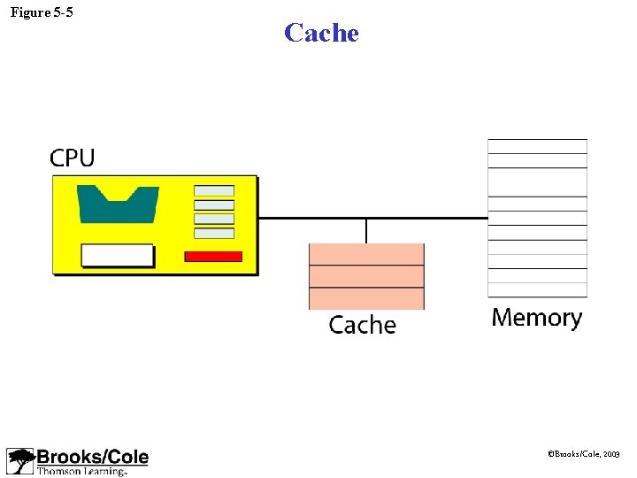
Figure 5 -5 Cache ©Brooks/Cole, 2003

5. 3 INPUT / OUTPUT ©Brooks/Cole, 2003
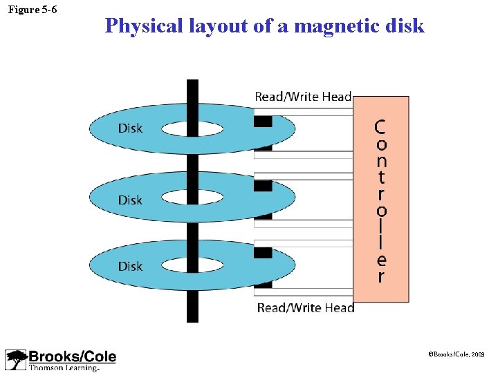
Figure 5 -6 Physical layout of a magnetic disk ©Brooks/Cole, 2003
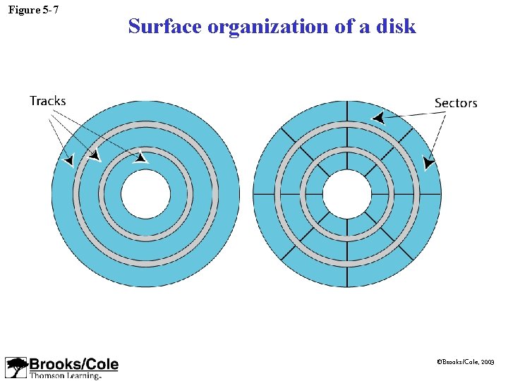
Figure 5 -7 Surface organization of a disk ©Brooks/Cole, 2003
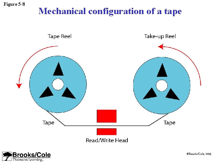
Figure 5 -8 Mechanical configuration of a tape ©Brooks/Cole, 2003
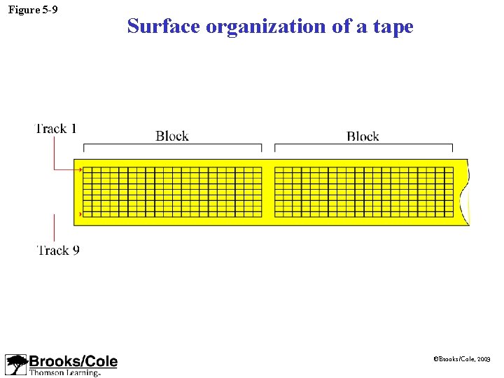
Figure 5 -9 Surface organization of a tape ©Brooks/Cole, 2003
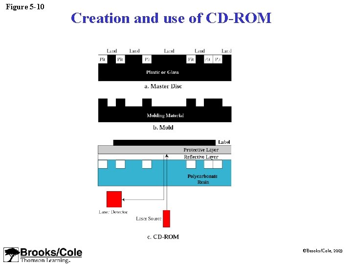
Figure 5 -10 Creation and use of CD-ROM ©Brooks/Cole, 2003
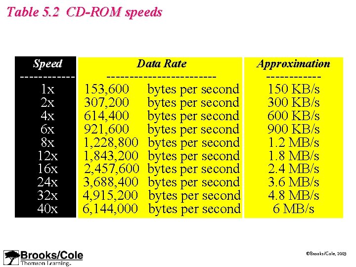
Table 5. 2 CD-ROM speeds Speed ------1 x 2 x 4 x 6 x 8 x 12 x 16 x 24 x 32 x 40 x Data Rate ------------153, 600 bytes per second 307, 200 bytes per second 614, 400 bytes per second 921, 600 bytes per second 1, 228, 800 bytes per second 1, 843, 200 bytes per second 2, 457, 600 bytes per second 3, 688, 400 bytes per second 4, 915, 200 bytes per second 6, 144, 000 bytes per second Approximation ------150 KB/s 300 KB/s 600 KB/s 900 KB/s 1. 2 MB/s 1. 8 MB/s 2. 4 MB/s 3. 6 MB/s 4. 8 MB/s 6 MB/s ©Brooks/Cole, 2003
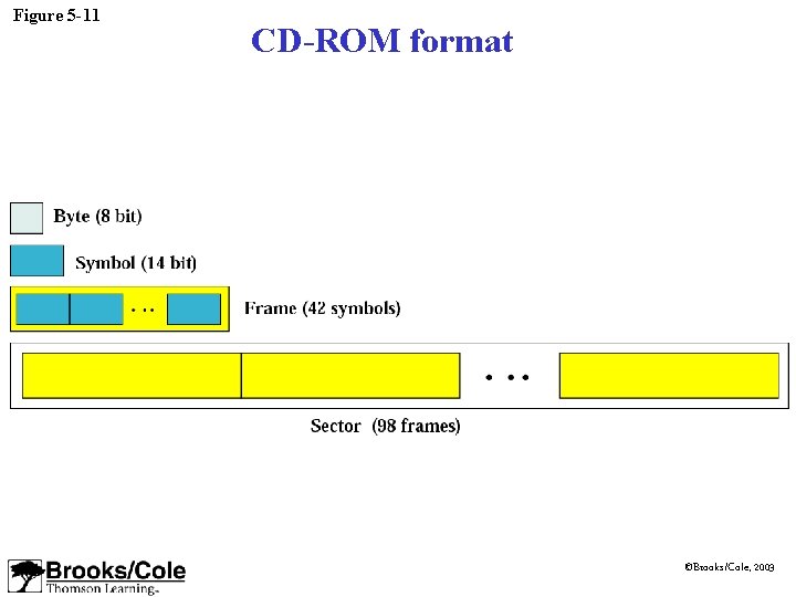
Figure 5 -11 CD-ROM format ©Brooks/Cole, 2003
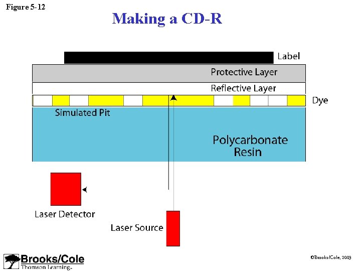
Figure 5 -12 Making a CD-R ©Brooks/Cole, 2003
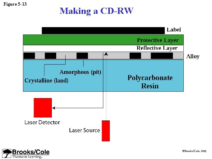
Figure 5 -13 Making a CD-RW ©Brooks/Cole, 2003
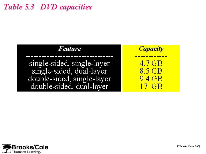
Table 5. 3 DVD capacities Feature ----------------single-sided, single-layer single-sided, dual-layer double-sided, single-layer double-sided, dual-layer Capacity ------4. 7 GB 8. 5 GB 9. 4 GB 17 GB ©Brooks/Cole, 2003
5. 4 SUBSYSTEM INTERCONNECTION ©Brooks/Cole, 2003
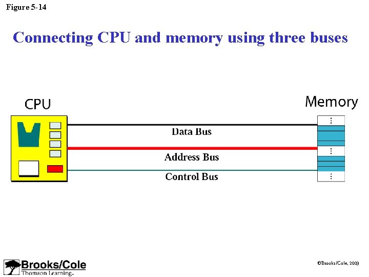
Figure 5 -14 Connecting CPU and memory using three buses ©Brooks/Cole, 2003
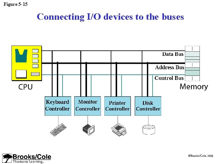
Figure 5 -15 Connecting I/O devices to the buses ©Brooks/Cole, 2003
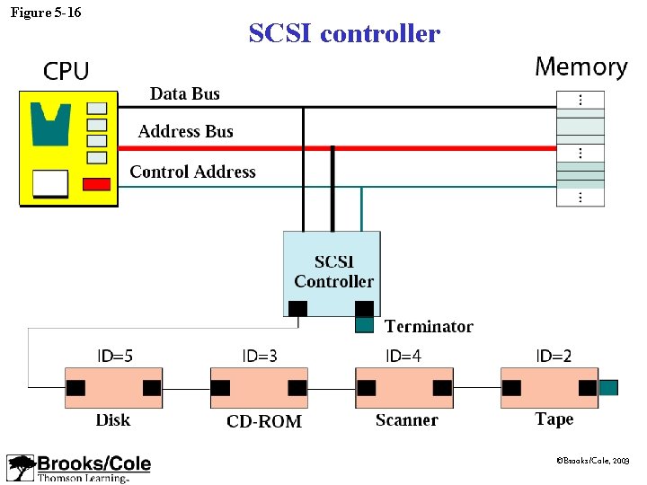
Figure 5 -16 SCSI controller ©Brooks/Cole, 2003
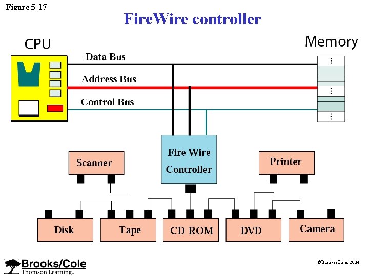
Figure 5 -17 Fire. Wire controller ©Brooks/Cole, 2003
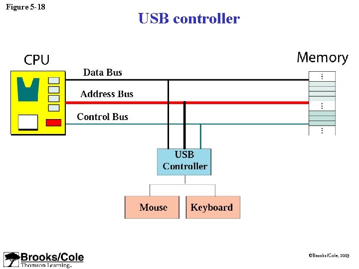
Figure 5 -18 USB controller ©Brooks/Cole, 2003
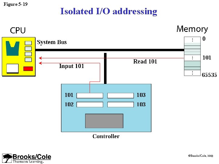
Figure 5 -19 Isolated I/O addressing ©Brooks/Cole, 2003
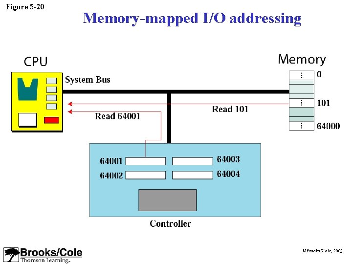
Figure 5 -20 Memory-mapped I/O addressing ©Brooks/Cole, 2003
5. 5 PROGRAM EXECUTION ©Brooks/Cole, 2003
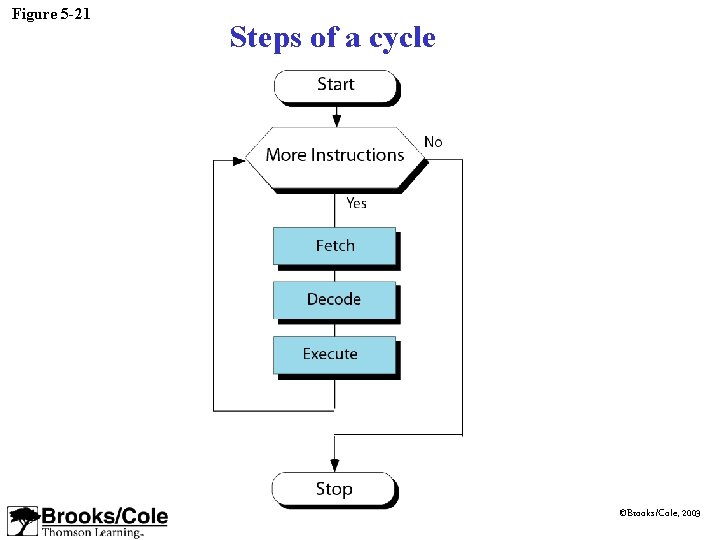
Figure 5 -21 Steps of a cycle ©Brooks/Cole, 2003
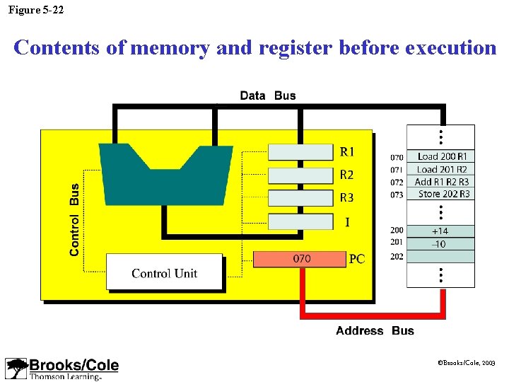
Figure 5 -22 Contents of memory and register before execution ©Brooks/Cole, 2003
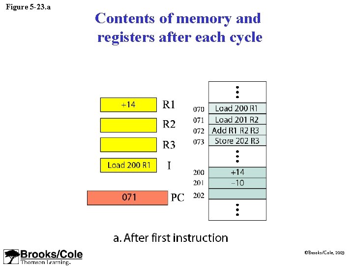
Figure 5 -23. a Contents of memory and registers after each cycle ©Brooks/Cole, 2003
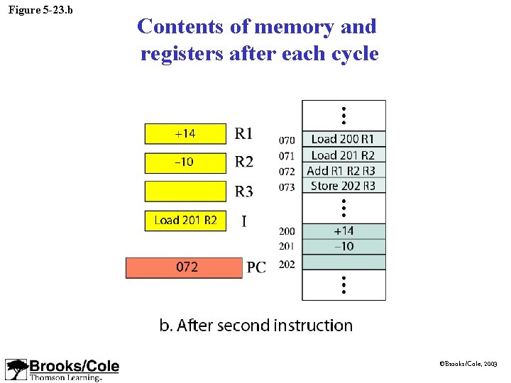
Figure 5 -23. b Contents of memory and registers after each cycle ©Brooks/Cole, 2003
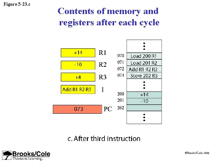
Figure 5 -23. c Contents of memory and registers after each cycle ©Brooks/Cole, 2003
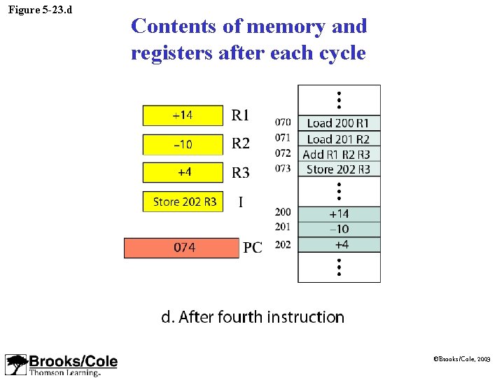
Figure 5 -23. d Contents of memory and registers after each cycle ©Brooks/Cole, 2003
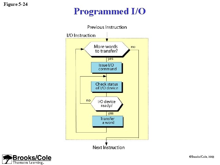
Figure 5 -24 Programmed I/O ©Brooks/Cole, 2003
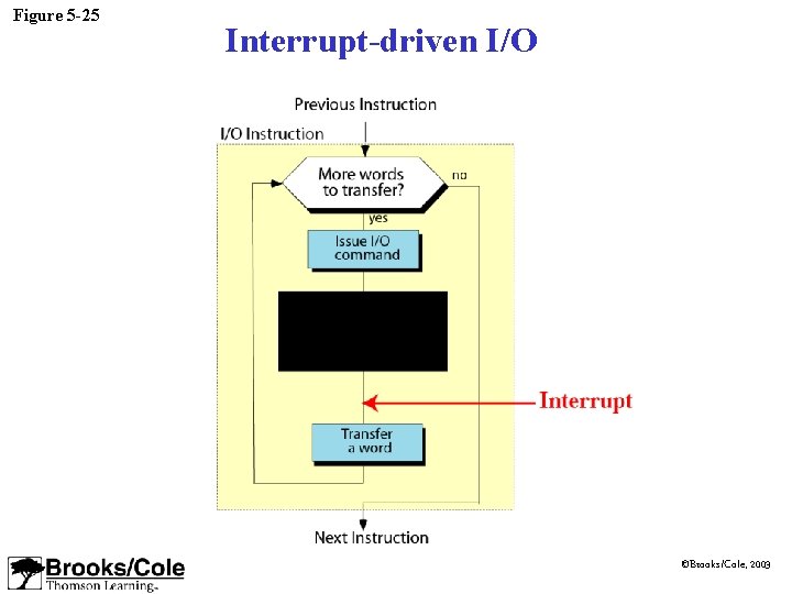
Figure 5 -25 Interrupt-driven I/O ©Brooks/Cole, 2003
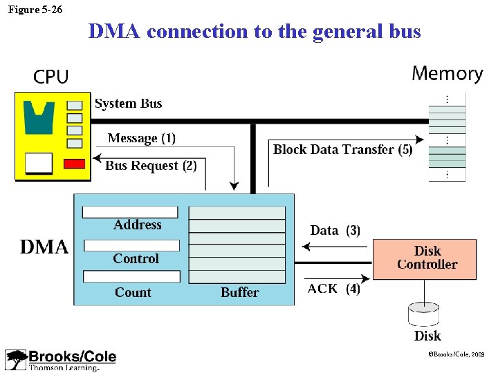
Figure 5 -26 DMA connection to the general bus ©Brooks/Cole, 2003
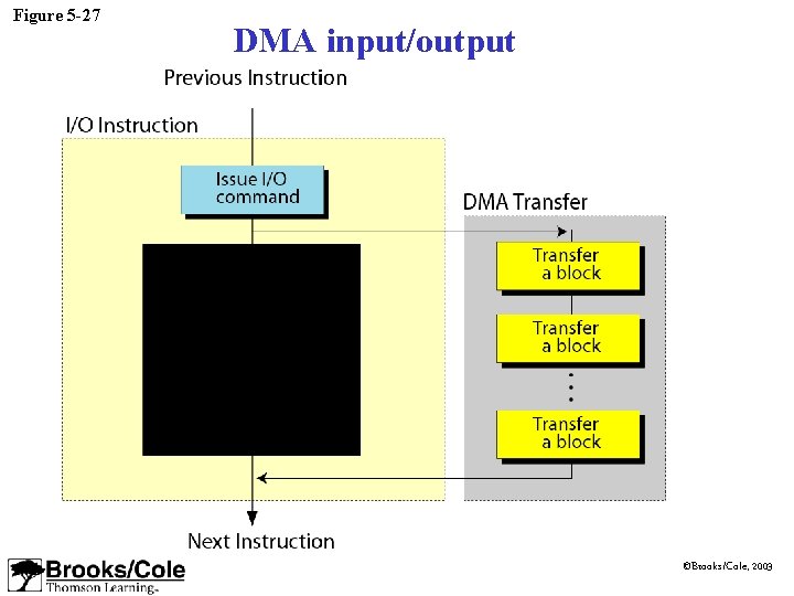
Figure 5 -27 DMA input/output ©Brooks/Cole, 2003
5. 6 TWO DIFFERENT ARCHITECTURES ©Brooks/Cole, 2003
- Slides: 45