Chapter 5 Combinational Logic By Taweesak Reungpeerakul 241
Chapter 5 Combinational Logic By Taweesak Reungpeerakul 241 -208 CH 5 1
Contents n n n 241 -208 CH 5 Basic Combinational Logic Circuits Implement SOP and POS using Basic Logic Gates Universal Property of NAND and NOR Combinational Logic using NAND and NOR Operation with Pulse Waveforms Digital System Application 2
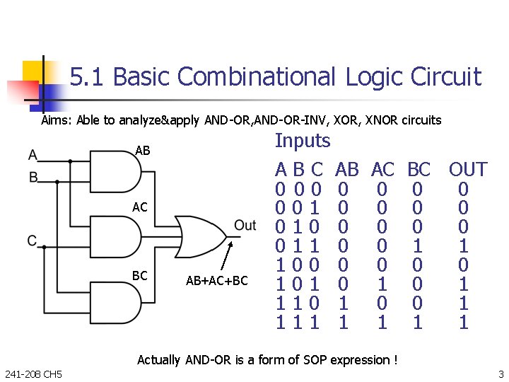
5. 1 Basic Combinational Logic Circuit Aims: Able to analyze&apply AND-OR, AND-OR-INV, XOR, XNOR circuits AB AC BC AB+AC+BC Inputs A B C AB 0 001 0 010 0 011 0 100 0 101 0 110 1 111 1 AC 0 0 0 1 BC OUT 0 0 0 1 1 1 Actually AND-OR is a form of SOP expression ! 241 -208 CH 5 3
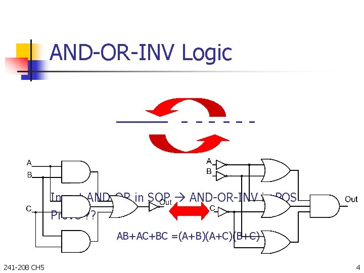
AND-OR-INV Logic Invert AND-OR in SOP AND-OR-INV in POS Prove ? ? AB+AC+BC =(A+B)(A+C)(B+C) 241 -208 CH 5 4
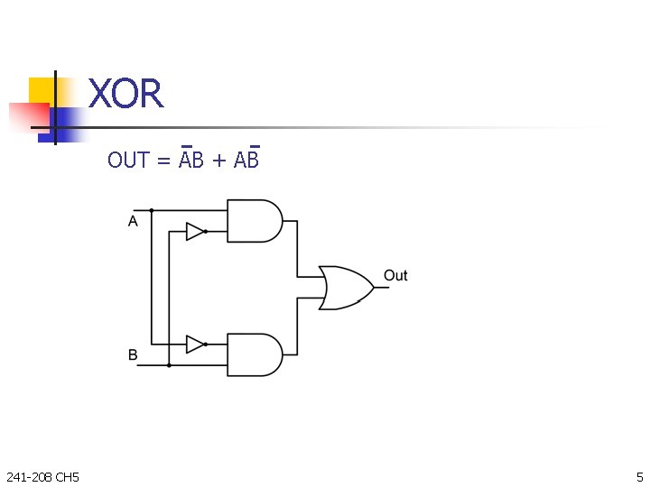
XOR OUT = AB + AB 241 -208 CH 5 5
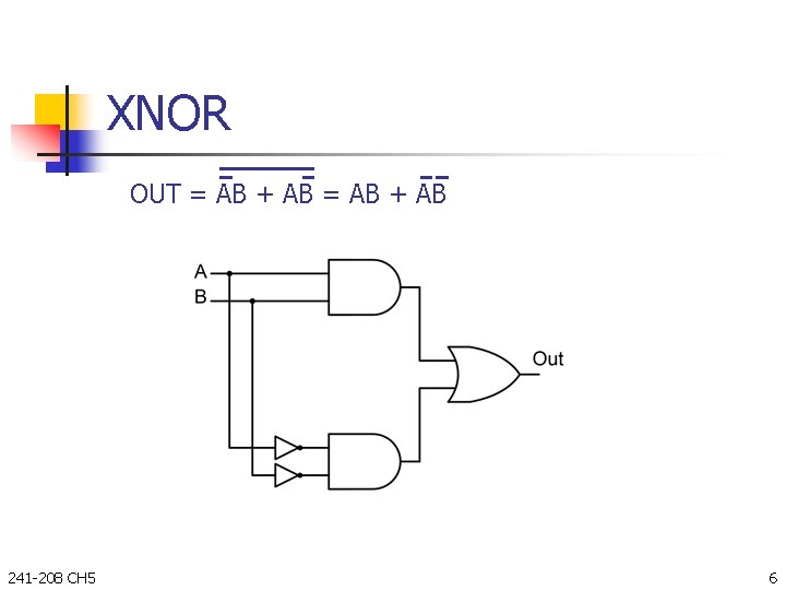
XNOR OUT = AB + AB 241 -208 CH 5 6
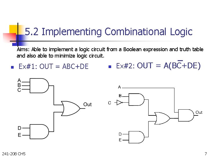
5. 2 Implementing Combinational Logic Aims: Able to implement a logic circuit from a Boolean expression and truth table and also able to minimize logic circuit. n Ex#1: OUT = ABC+DE 241 -208 CH 5 n Ex#2: OUT = A(BC+DE) 7
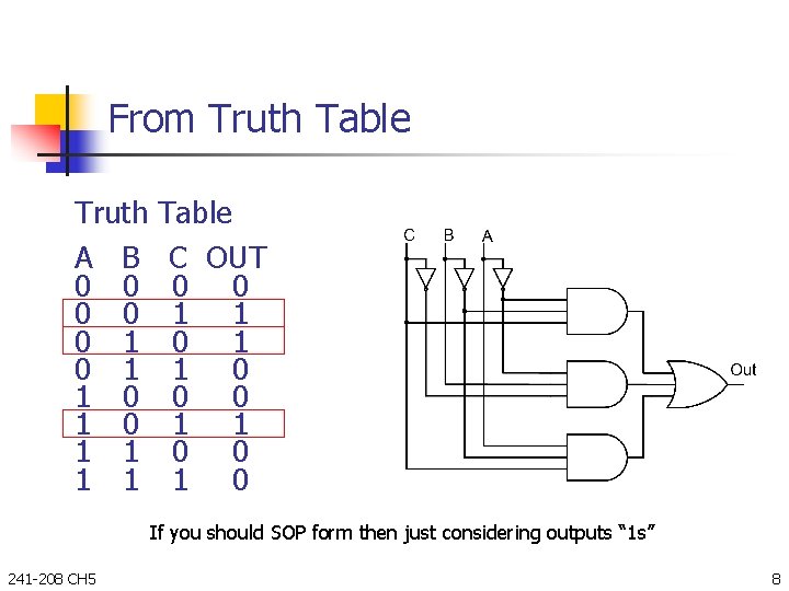
From Truth Table Truth A B 0 0 0 1 0 1 1 1 1 Table C OUT 0 0 1 1 0 0 1 0 If you should SOP form then just considering outputs “ 1 s” 241 -208 CH 5 8
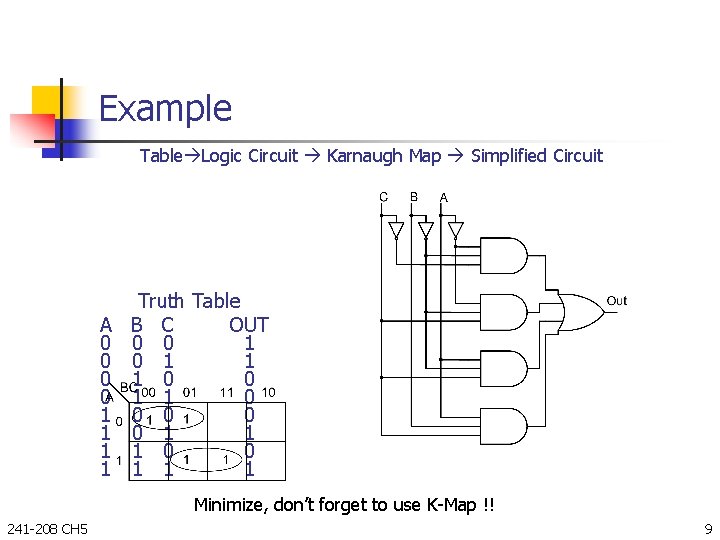
Example Table Logic Circuit Karnaugh Map Simplified Circuit A 0 0 1 1 Truth Table B C OUT 0 0 1 1 1 0 0 0 0 0 1 1 1 Minimize, don’t forget to use K-Map !! 241 -208 CH 5 9
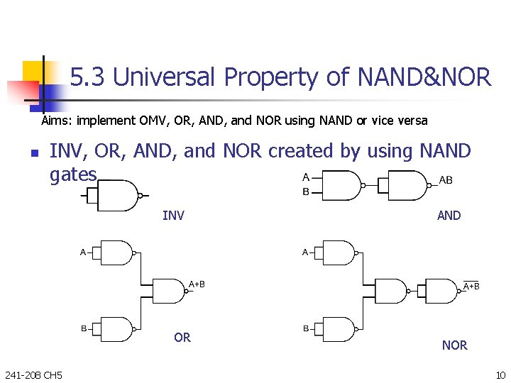
5. 3 Universal Property of NAND&NOR Aims: implement OMV, OR, AND, and NOR using NAND or vice versa n INV, OR, AND, and NOR created by using NAND gates INV OR 241 -208 CH 5 AND NOR 10
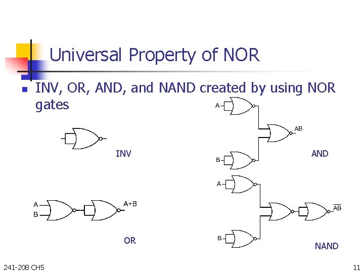
Universal Property of NOR n INV, OR, AND, and NAND created by using NOR gates INV OR 241 -208 CH 5 AND NAND 11
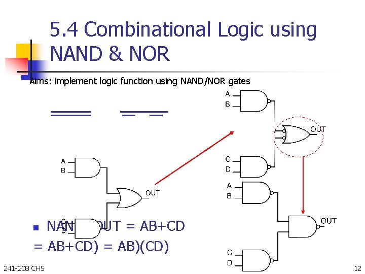
5. 4 Combinational Logic using NAND & NOR Aims: implement logic function using NAND/NOR gates NAND; OUT = AB+CD) = AB)(CD) n 241 -208 CH 5 12
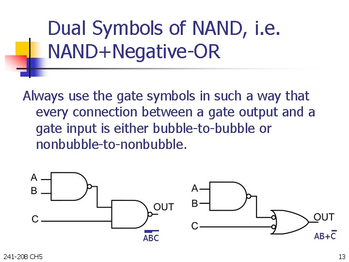
Dual Symbols of NAND, i. e. NAND+Negative-OR Always use the gate symbols in such a way that every connection between a gate output and a gate input is either bubble-to-bubble or nonbubble-to-nonbubble. ABC 241 -208 CH 5 AB+C 13
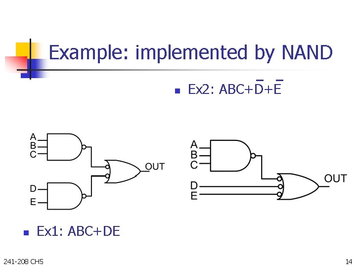
Example: implemented by NAND n n Ex 2: ABC+D+E Ex 1: ABC+DE 241 -208 CH 5 14
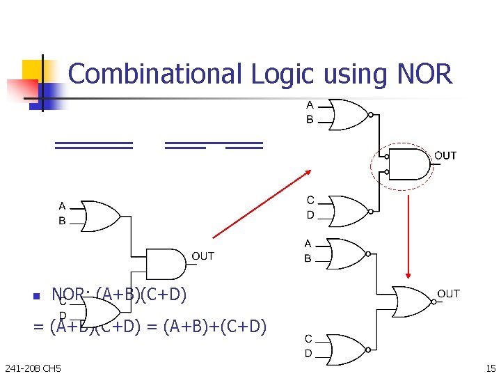
Combinational Logic using NOR n NOR; (A+B)(C+D) = (A+B)+(C+D) 241 -208 CH 5 15
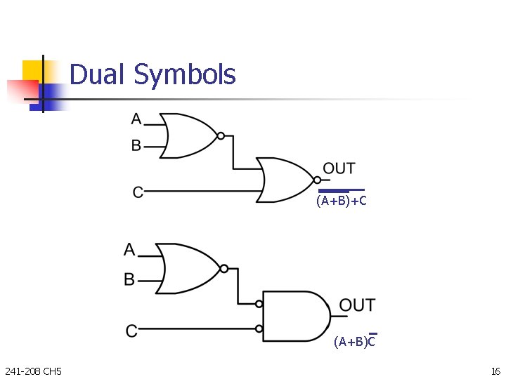
Dual Symbols (A+B)+C (A+B)C 241 -208 CH 5 16
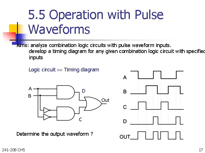
5. 5 Operation with Pulse Waveforms Aims: analyze combination logic circuits with pulse waveform inputs. develop a timing diagram for any given combination logic circuit with specified inputs Logic circuit Timing diagram D C Determine the output waveform ? 241 -208 CH 5 17
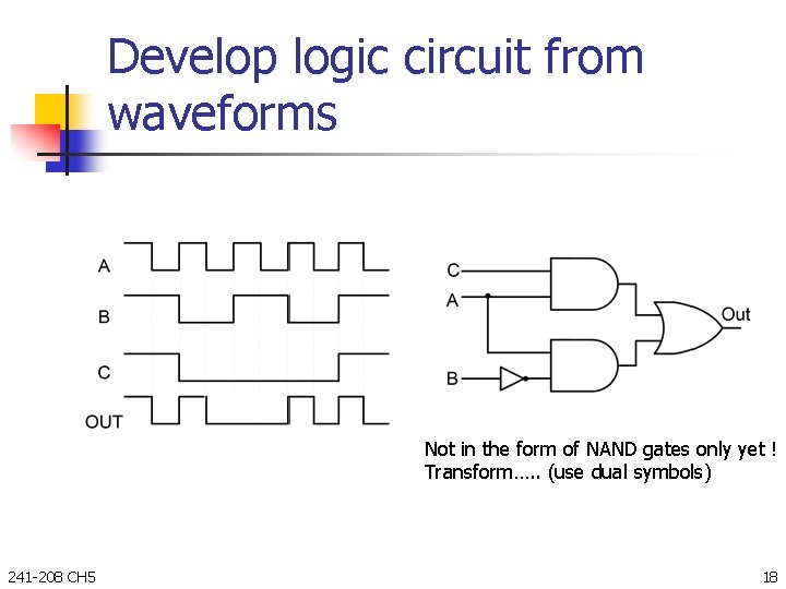
Develop logic circuit from waveforms Not in the form of NAND gates only yet ! Transform…. . (use dual symbols) 241 -208 CH 5 18
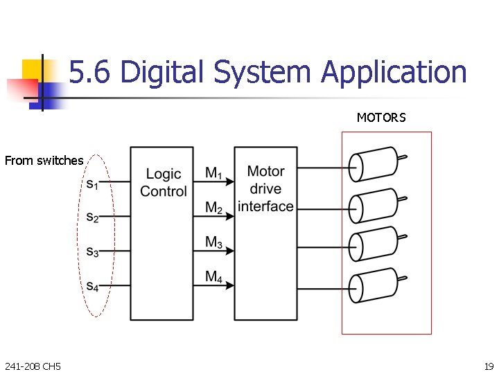
5. 6 Digital System Application MOTORS From switches 241 -208 CH 5 19
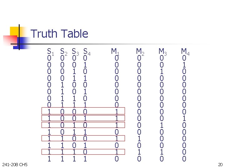
Truth Table 241 -208 CH 5 S 1 0 0 0 0 1 1 1 1 S 2 0 0 0 0 1 1 1 1 S 3 0 0 1 1 S 4 0 1 0 1 M 1 0 0 0 0 1 1 1 0 1 0 M 2 0 0 0 1 0 M 3 0 0 1 0 0 0 1 0 M 4 0 1 0 0 0 20
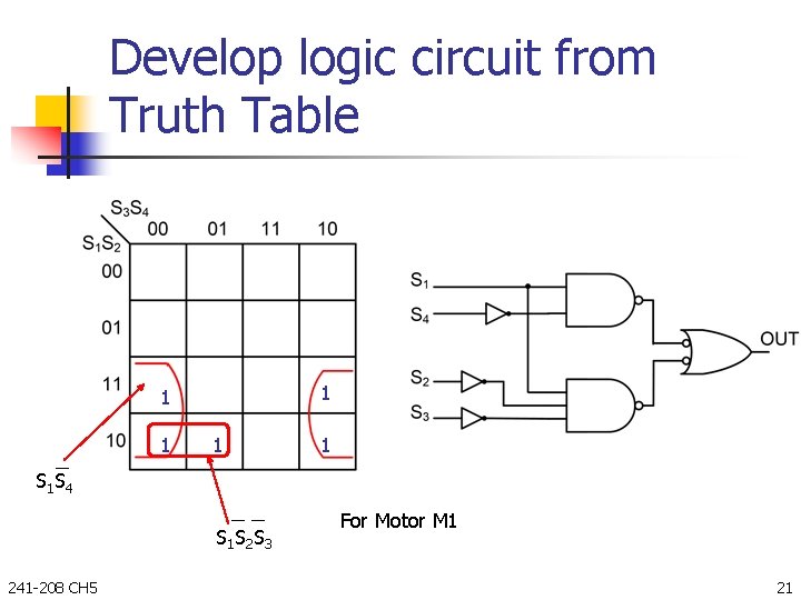
Develop logic circuit from Truth Table 1 1 1 S 4 S 1 S 2 S 3 241 -208 CH 5 For Motor M 1 21
- Slides: 21