Chapter 4 SYSTEM DESIGN Requirement Analysis What is
- Slides: 26

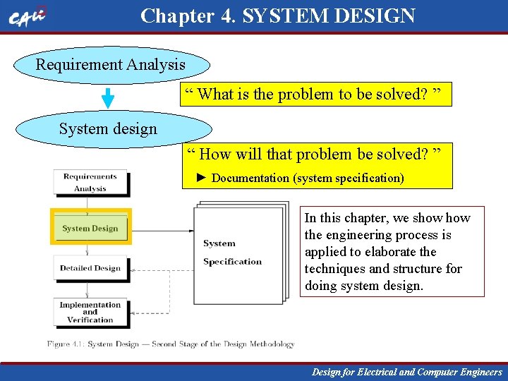
Chapter 4. SYSTEM DESIGN Requirement Analysis “ What is the problem to be solved? ” System design “ How will that problem be solved? ” ► Documentation (system specification) In this chapter, we show the engineering process is applied to elaborate the techniques and structure for doing system design. Design for Electrical and Computer Engineers

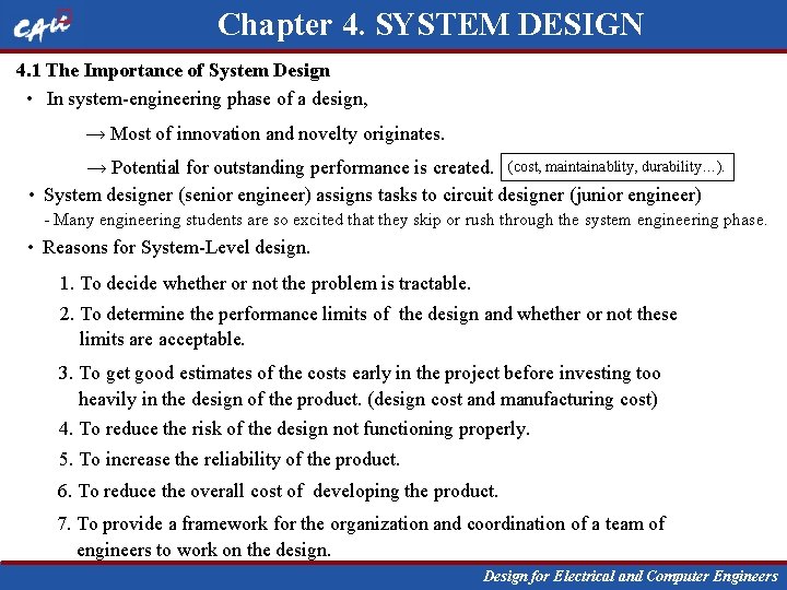
Chapter 4. SYSTEM DESIGN 4. 1 The Importance of System Design • In system-engineering phase of a design, → Most of innovation and novelty originates. → Potential for outstanding performance is created. (cost, maintainablity, durability…). • System designer (senior engineer) assigns tasks to circuit designer (junior engineer) - Many engineering students are so excited that they skip or rush through the system engineering phase. • Reasons for System-Level design. 1. To decide whether or not the problem is tractable. 2. To determine the performance limits of the design and whether or not these limits are acceptable. 3. To get good estimates of the costs early in the project before investing too heavily in the design of the product. (design cost and manufacturing cost) 4. To reduce the risk of the design not functioning properly. 5. To increase the reliability of the product. 6. To reduce the overall cost of developing the product. 7. To provide a framework for the organization and coordination of a team of engineers to work on the design. Design for Electrical and Computer Engineers

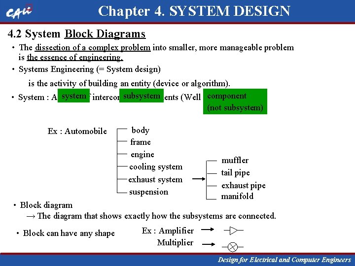
Chapter 4. SYSTEM DESIGN 4. 2 System Block Diagrams • The dissection of a complex problem into smaller, more manageable problem is the essence of engineering. • Systems Engineering (= System design) is the activity of building an entity (device or algorithm). systemof interconnected subsystem component • System : A group elements (Well defined function) (not subsystem) Ex : Automobile body frame engine cooling system exhaust system suspension muffler tail pipe exhaust pipe manifold • Block diagram → The diagram that shows exactly how the subsystems are connected. • Block can have any shape Ex : Amplifier Multiplier Design for Electrical and Computer Engineers

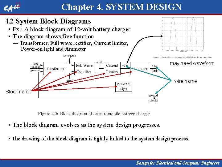
Chapter 4. SYSTEM DESIGN 4. 2 System Block Diagrams • Ex : A block diagram of 12 -volt battery charger • The diagram shows five function → Transformer, Full wave rectifier, Current limiter, Power-on light and Ammeter may need waveform wire name Block name • The block diagram evolves as the system design progresses. • The drawing of the block diagram is tightly linked to the system design process. Design for Electrical and Computer Engineers

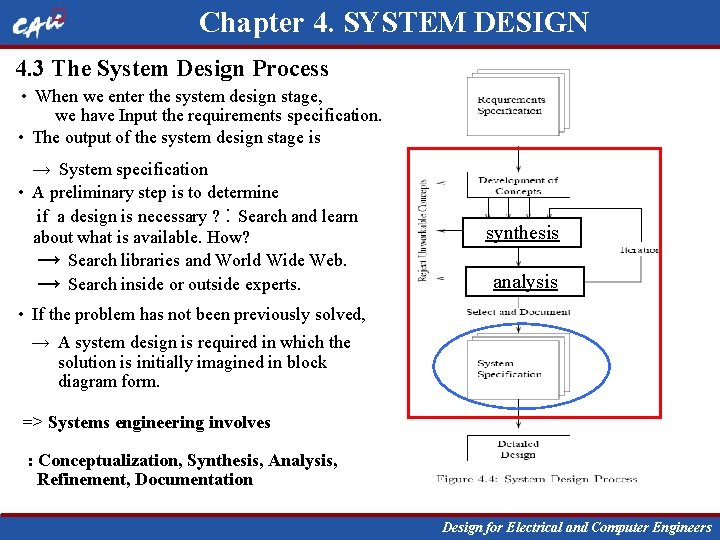
Chapter 4. SYSTEM DESIGN 4. 3 The System Design Process • When we enter the system design stage, we have Input the requirements specification. • The output of the system design stage is → System specification • A preliminary step is to determine if a design is necessary ? : Search and learn about what is available. How? → Search libraries and World Wide Web. → Search inside or outside experts. synthesis analysis • If the problem has not been previously solved, → A system design is required in which the solution is initially imagined in block diagram form. => Systems engineering involves : Conceptualization, Synthesis, Analysis, Refinement, Documentation Design for Electrical and Computer Engineers

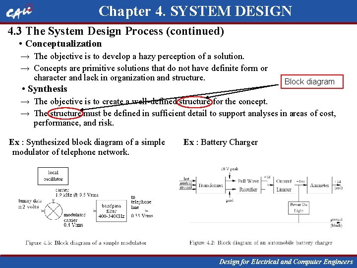
Chapter 4. SYSTEM DESIGN 4. 3 The System Design Process (continued) • Conceptualization → The objective is to develop a hazy perception of a solution. → Concepts are primitive solutions that do not have definite form or character and lack in organization and structure. • Synthesis Block diagram → The objective is to create a well-defined structure for the concept. → The structure must be defined in sufficient detail to support analyses in areas of cost, performance, and risk. Ex : Synthesized block diagram of a simple modulator of telephone network. Ex : Battery Charger Design for Electrical and Computer Engineers

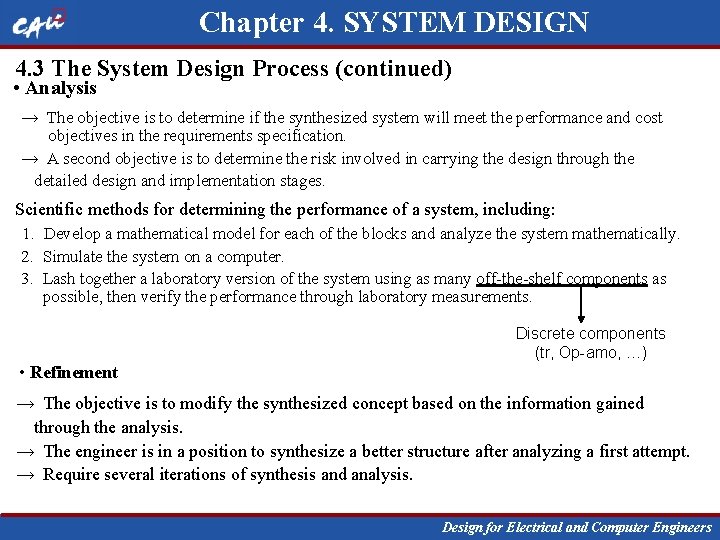
Chapter 4. SYSTEM DESIGN 4. 3 The System Design Process (continued) • Analysis → The objective is to determine if the synthesized system will meet the performance and cost objectives in the requirements specification. → A second objective is to determine the risk involved in carrying the design through the detailed design and implementation stages. Scientific methods for determining the performance of a system, including: 1. Develop a mathematical model for each of the blocks and analyze the system mathematically. 2. Simulate the system on a computer. 3. Lash together a laboratory version of the system using as many off-the-shelf components as possible, then verify the performance through laboratory measurements. • Refinement Discrete components (tr, Op-amo, …) → The objective is to modify the synthesized concept based on the information gained through the analysis. → The engineer is in a position to synthesize a better structure after analyzing a first attempt. → Require several iterations of synthesis and analysis. Design for Electrical and Computer Engineers

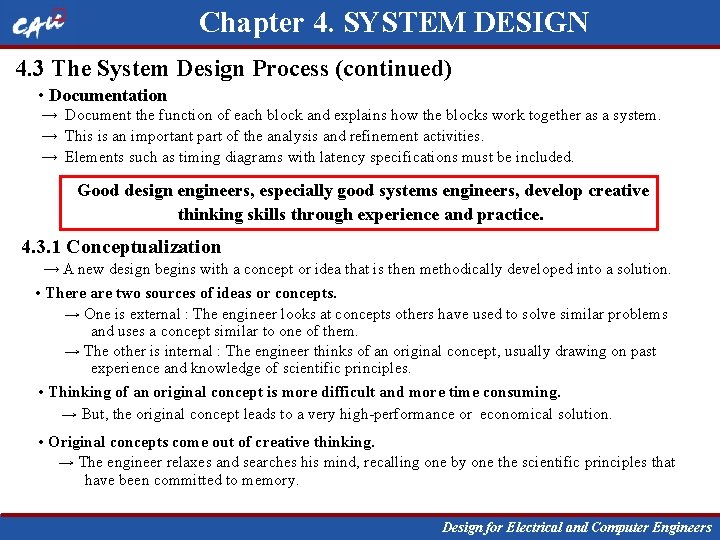
Chapter 4. SYSTEM DESIGN 4. 3 The System Design Process (continued) • Documentation → Document the function of each block and explains how the blocks work together as a system. → This is an important part of the analysis and refinement activities. → Elements such as timing diagrams with latency specifications must be included. Good design engineers, especially good systems engineers, develop creative thinking skills through experience and practice. 4. 3. 1 Conceptualization → A new design begins with a concept or idea that is then methodically developed into a solution. • There are two sources of ideas or concepts. → One is external : The engineer looks at concepts others have used to solve similar problems and uses a concept similar to one of them. → The other is internal : The engineer thinks of an original concept, usually drawing on past experience and knowledge of scientific principles. • Thinking of an original concept is more difficult and more time consuming. → But, the original concept leads to a very high-performance or economical solution. • Original concepts come out of creative thinking. → The engineer relaxes and searches his mind, recalling one by one the scientific principles that have been committed to memory. Design for Electrical and Computer Engineers

Chapter 4. SYSTEM DESIGN 4. 3 The System Design Process 4. 3. 1 Conceptualization (example) • The problem of measuring the speed of a baseball 1. A radio wave experiences a Doppler shift when it is reflected from a moving object. 2. The velocity of an object is inversely proportional to the time it takes to travel a set distance. 3. The size of the image in a video camera depends on the distance between the object and the camera. 4. The momentum of an object is proportional to its velocity. 5. Bernoulli’s law relates velocity to pressure. 6. The trajectory of a projectile in a gravitational field is parabolic, with the curvature depending on the horizontal velocity of the projectile. Which one is better? (Performance, cost, maintainabilty, reliability. ) To determine, you need knowledge. That’s why you study hard!!! Design for Electrical and Computer Engineers

Chapter 4. SYSTEM DESIGN 4. 3. 2 Synthesis : the process of bringing structure to the initial concept. • There are two conflicting forces that drive the design process. → One is the need to have design completed quickly. → The other is the need for a novel solution that offers either a cost or performance advantage over the competition. • The goal is to interpolate or extrapolate a reference design to produce one that solves the problem. → Adapting an existing design to fit the problem at hand is often done with straightforward, logical reasoning. • But, synthesis driven by linear thinking does not offer great hope for drastically reducing cost or improving performance. → However, it is the most economical and reliable approach an the most commonly used. 4. 3. 3 Analysis : taught in most engineering classes. • There are many tools available for analysis → Such as MATLAB for mathematical analysis and SIMULINK for the simulation of block diagrams. Design for Electrical and Computer Engineers

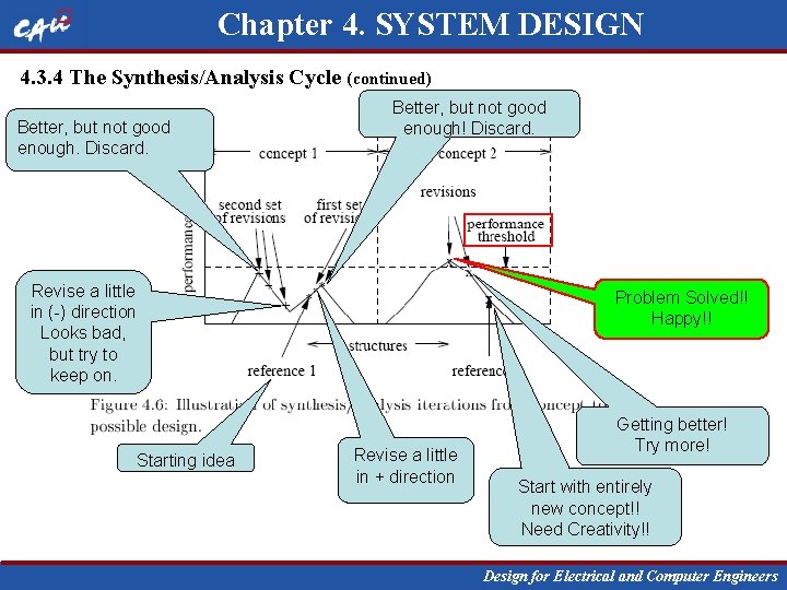
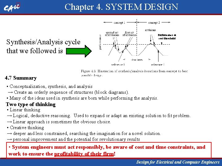
Chapter 4. SYSTEM DESIGN 4. 3. 4 The Synthesis/Analysis Cycle • Refinement of the design and elaboration of the block diagram take place through an iterative cycle of synthesis and analysis. • To be successful, an engineer must be willing to synthesize structures for concept after concept until one is found whose deficiencies can be corrected. • The analysis of the structure is put on paper. This will be a logical argument supported with mathematics, computer simulation, and laboratory tests. When the structure is not good enough and the engineer is out of ideas for improvement, if he or she decides to push on, there are three ways to proceed: 1. Go back to the structure first synthesized from the concept and look at modifying it in a different way in hopes that the synthesis/analysis iterations will lead to a structure that meets the cost and performance objectives. 2. Synthesize a new structure from the same concept. 3. Use creative thinking to conceive a new concept and then synthesize a structure used on this concept. Design for Electrical and Computer Engineers

Chapter 4. SYSTEM DESIGN 4. 3. 4 The Synthesis/Analysis Cycle (continued) Better, but not good enough. Discard. Better, but not good enough! Discard. Revise a little in (-) direction Looks bad, but try to keep on. Starting idea Problem Solved!! Happy!! Revise a little in + direction Getting better! Try more! Start with entirely new concept!! Need Creativity!! Design for Electrical and Computer Engineers

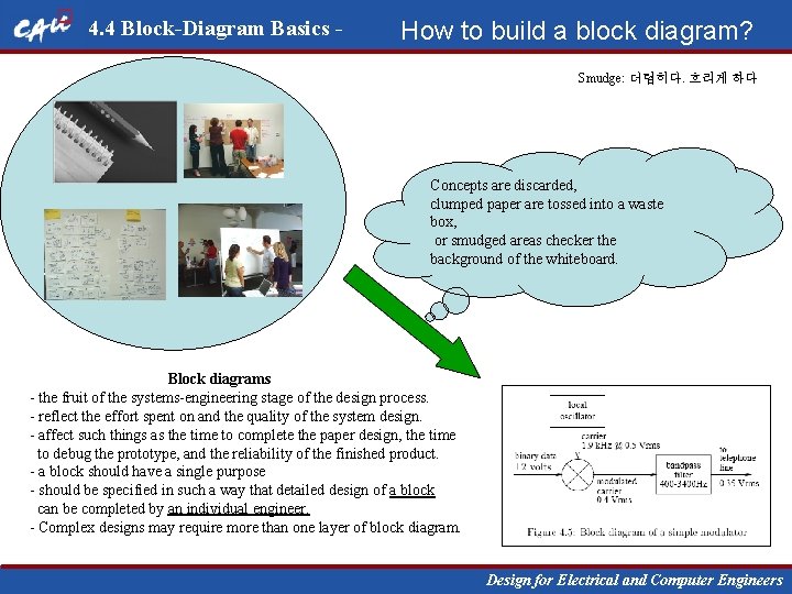
4. 4 Block-Diagram Basics - How to build a block diagram? Smudge: 더럽히다. 흐리게 하다 Concepts are discarded, clumped paper are tossed into a waste box, or smudged areas checker the background of the whiteboard. Block diagrams - the fruit of the systems-engineering stage of the design process. - reflect the effort spent on and the quality of the system design. - affect such things as the time to complete the paper design, the time to debug the prototype, and the reliability of the finished product. - a block should have a single purpose - should be specified in such a way that detailed design of a block can be completed by an individual engineer. - Complex designs may require more than one layer of block diagram. Design for Electrical and Computer Engineers

Capstone (절정, 극치, 건축에서 마지막에 올리는 돌) Design What is capstone design? Capstone Design applies the engineering sciences to the design of a system, component or process. Students choose the particular design project with approval of appropriate faculty. Design teams are organized. Each project includes the use of open-ended problems, development and use of design methodology, formulation of design problem statements and specification, consideration of alternative solutions, feasibility consideration and detailed system descriptions. It also includes realistic constraints (such as economic factors and social impact). Capstone Design 공학계열의 학생이 이론과 실습위주의 교육에서 벗어나 실무 에서 접하는 문제를 해결할 수 있도록 학부에서 배운 지식을 바 탕으로 팀을 구성하고 제품을 기획, 설계, 제작하는 종합설계과 목이다. Design for Electrical and Computer Engineers

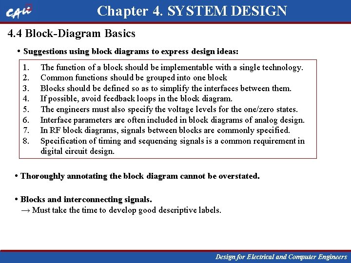
Chapter 4. SYSTEM DESIGN 4. 4 Block-Diagram Basics • Suggestions using block diagrams to express design ideas: 1. 2. 3. 4. 5. 6. 7. 8. The function of a block should be implementable with a single technology. Common functions should be grouped into one block Blocks should be defined so as to simplify the interfaces between them. If possible, avoid feedback loops in the block diagram. The engineers must also specify the voltage levels for the one/zero states. Interface parameters are often included in block diagrams of analog design. In RF block diagrams, signals between blocks are commonly specified. Specification of timing and sequencing signals is a common requirement in digital circuit design. • Thoroughly annotating the block diagram cannot be overstated. • Blocks and interconnecting signals. → Must take the time to develop good descriptive labels. Design for Electrical and Computer Engineers

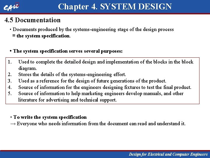
Chapter 4. SYSTEM DESIGN 4. 5 Documentation • Documents produced by the systems-engineering stage of the design process = the system specification. • The system specification serves several purposes: 1. 2. 3. 4. 5. Used to complete the detailed design and implementation of the blocks in the block diagram. Stores the details of the systems-engineering effort. Used as a reference for the design of future generations of the product. Source of information for the engineers designing fixtures to test the final product. Source of information to help marketing engineers develop manuals, and other literature for advertising and technical support. • To write the system specification → Everyone who needs information from the document can read and understand it. Design for Electrical and Computer Engineers

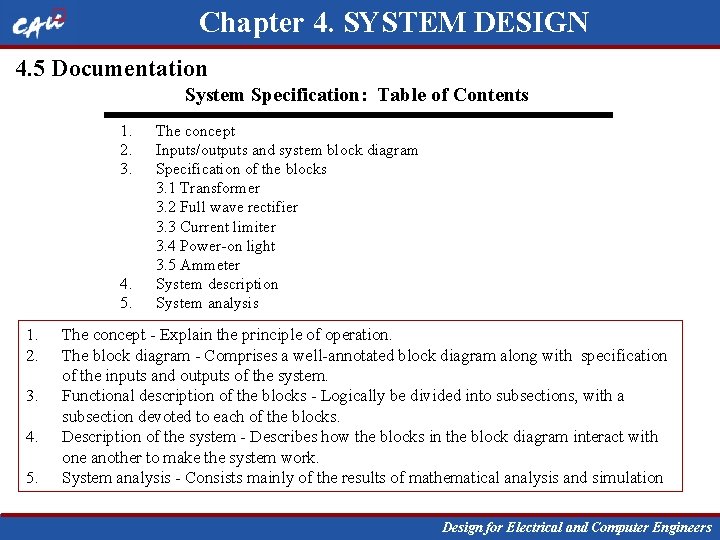
Chapter 4. SYSTEM DESIGN 4. 5 Documentation System Specification: Table of Contents 1. 2. 3. 4. 5. 1. 2. 3. 4. 5. The concept Inputs/outputs and system block diagram Specification of the blocks 3. 1 Transformer 3. 2 Full wave rectifier 3. 3 Current limiter 3. 4 Power-on light 3. 5 Ammeter System description System analysis The concept - Explain the principle of operation. The block diagram - Comprises a well-annotated block diagram along with specification of the inputs and outputs of the system. Functional description of the blocks - Logically be divided into subsections, with a subsection devoted to each of the blocks. Description of the system - Describes how the blocks in the block diagram interact with one another to make the system work. System analysis - Consists mainly of the results of mathematical analysis and simulation Design for Electrical and Computer Engineers

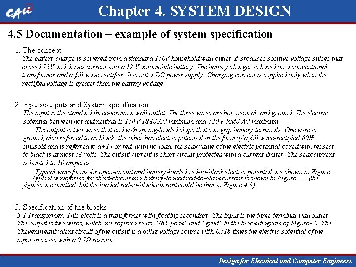
Chapter 4. SYSTEM DESIGN 4. 5 Documentation – example of system specification 1. The concept The battery charge is powered from a standard 110 V household wall outlet. It produces positive voltage pulses that exceed 12 V and drives current into a 12 V automobile battery. The battery charger is based on a conventional transformer and a full wave rectifier. It is not a DC power supply. Charging current is supplied only when the rectified voltage is greater than the battery voltage. 2. Inputs/outputs and System specification The input is the standard three-terminal wall outlet. The three wires are hot, neutral, and ground. The electric potential between hot and neutral is 110 V RMS AC minimum and 120 V RMS AC maximum. The output is two wires that end with spring-loaded claps that can grip battery terminals. One wire is ground, also referred to as black: the other has electric potential in the form of a full wave-rectified 60 Hz sinusoid and is referred to a+14 or red. With no load, the peak value of the electric potential of red with respect to black is at most 18 volts. The output current is short-circuit protected with a current limiter. The peak current is limited to 10 amperes. Typical waveforms for open-circuit and battery-loaded red-to-black electric potential are shown in Figure · · ·. Typical waveforms for short-circuit and battery-loaded red-to-black current is shown in Figure · · · (the figures are omitted, but the loaded red-to-black current could be that in Figure 4. 3). 3. Specification of the blocks 3. 1 Transformer: This block is a transformer with floating secondary. The input is the three-terminal wall outlet. The output is two wires, which are referred to as “ 18 V peak” and “grnd” in the block diagram of Figure 4. 2. Thevenin equivalent circuit of the output is a 60 Hz voltage source with 0. 118 times the electric potential of the input in series with a 0. 1Ω resistor. Design for Electrical and Computer Engineers

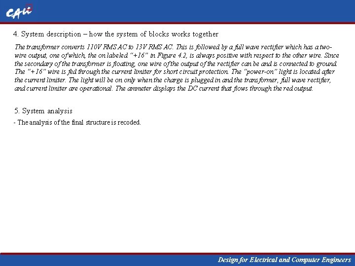
4. System description – how the system of blocks works together The transformer converts 110 V RMS AC to 13 V RMS AC. This is followed by a full wave rectifier which has a twowire output, one of which, the on labeled “+16” in Figure 4. 2, is always positive with respect to the other wire. Since the secondary of the transformer is floating, one wire of the output of the rectifier can be and is connected to ground. The “+16” wire is fed through the current limiter for short circuit protection. The “power-on” light is located after the current limiter. The light will be on only when the charge is plugged in and the transformer, full wave rectifier, and current limiter are operational. The ammeter displays the DC current that flows through the red output. 5. System analysis - The analysis of the final structure is recoded. Design for Electrical and Computer Engineers

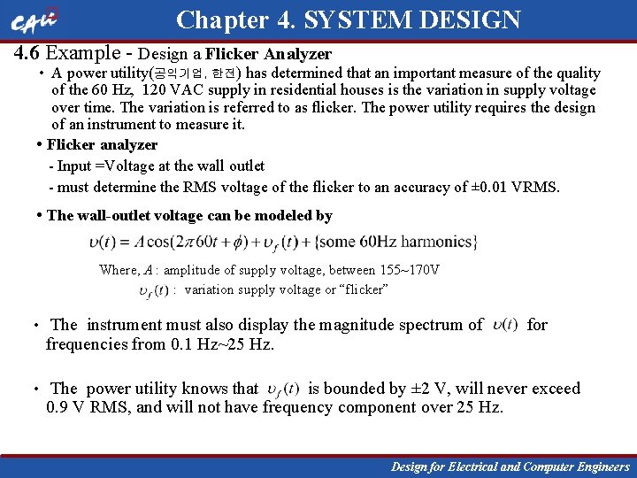
Chapter 4. SYSTEM DESIGN 4. 6 Example - Design a Flicker Analyzer • A power utility(공익기업, 한전) has determined that an important measure of the quality of the 60 Hz, 120 VAC supply in residential houses is the variation in supply voltage over time. The variation is referred to as flicker. The power utility requires the design of an instrument to measure it. • Flicker analyzer - Input =Voltage at the wall outlet - must determine the RMS voltage of the flicker to an accuracy of ± 0. 01 VRMS. • The wall-outlet voltage can be modeled by Where, A : amplitude of supply voltage, between 155~170 V : variation supply voltage or “flicker” • The instrument must also display the magnitude spectrum of frequencies from 0. 1 Hz~25 Hz. for • The power utility knows that is bounded by ± 2 V, will never exceed 0. 9 V RMS, and will not have frequency component over 25 Hz. Design for Electrical and Computer Engineers

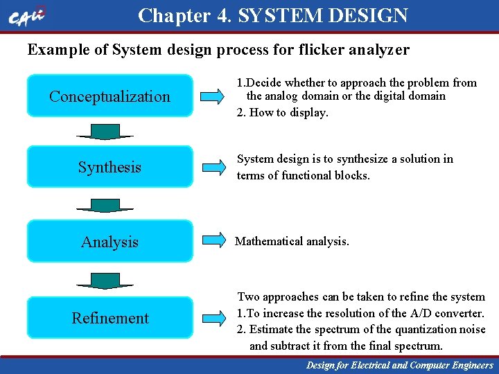
Chapter 4. SYSTEM DESIGN Example of System design process for flicker analyzer Conceptualization 1. Decide whether to approach the problem from the analog domain or the digital domain 2. How to display. Synthesis System design is to synthesize a solution in terms of functional blocks. Analysis Mathematical analysis. Refinement Two approaches can be taken to refine the system 1. To increase the resolution of the A/D converter. 2. Estimate the spectrum of the quantization noise and subtract it from the final spectrum. Design for Electrical and Computer Engineers

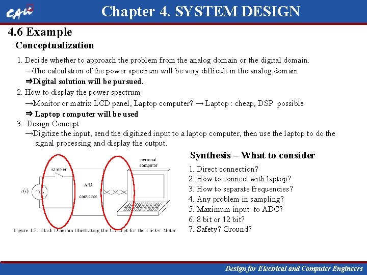
Chapter 4. SYSTEM DESIGN 4. 6 Example Conceptualization 1. Decide whether to approach the problem from the analog domain or the digital domain. →The calculation of the power spectrum will be very difficult in the analog domain ⇒Digital solution will be pursued. 2. How to display the power spectrum →Monitor or matrix LCD panel, Laptop computer? → Laptop : cheap, DSP possible ⇒ Laptop computer will be used 3. Design Concept →Digitize the input, send the digitized input to a laptop computer, then use the laptop to do the signal processing and display the output. Synthesis – What to consider 1. Direct connection? 2. How to connect with laptop? 3. How to separate frequencies? 4. Any problem in sampling? 5. Maximum input to ADC? 6. 8 bit or 12 bit? 7. Safety? Ground? Design for Electrical and Computer Engineers

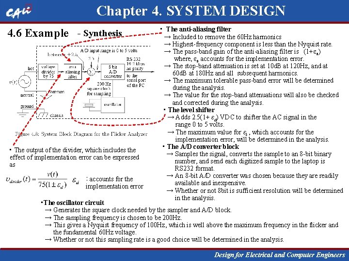
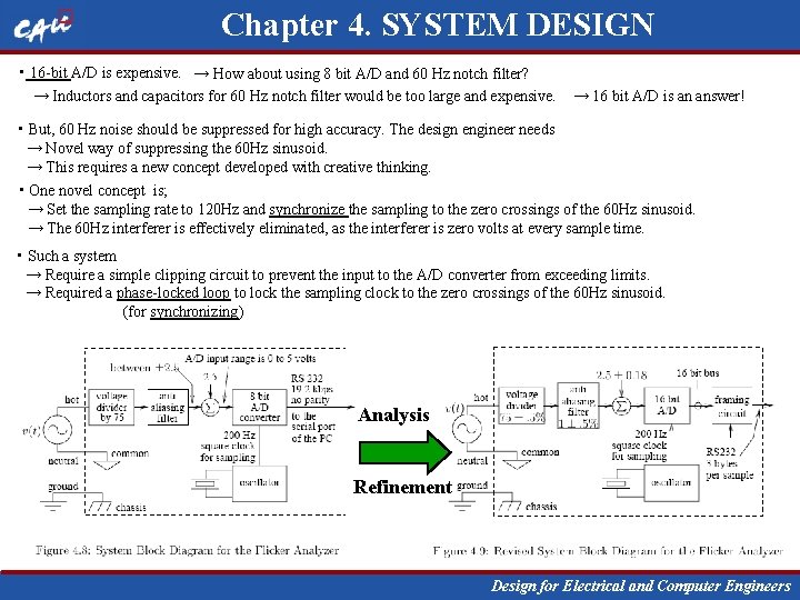
Chapter 4. SYSTEM DESIGN 4. 6 Example - Synthesis • The output of the divider, which includes the effect of implementation error can be expressed as : accounts for the implementation error • The anti-aliasing filter → Included to remove the 60 Hz harmonics → Highest-frequency component is less than the Nyquist rate. → The pass-band gain of the anti-aliasing filter is (1+εa) where, εa accounts for the implementation error. → The stop-band attenuation is set at 10 d. B at 120 Hz, and at 60 d. B at 180 Hz and all subsequent harmonics. → The maximum tolerable pass-band error will be determined during the analysis. → The value for the stop-band attenuations will also be checked and corrected during the analysis. • The level shifter → Adds 2. 5(1+ εd) VDC to shifter the AC signal in the range 0 to 5 volts. → The maximum value for εl , which accounts for the implementation error, will be determined in the analysis. • The A/D converter block → Samples the signal, converts the sample to an 8 -bit binary number, and send each digitized sample to the laptop is RS 232 format. → An 8 -bit A/D converter was chosen because they are readily available and inexpensive. → Whether or not 8 bit is sufficient resolution will be determined in the analysis. • The oscillator circuit → Generates the square clock needed by the sampler and A/D block. → The sampling frequency is chosen to be 200 Hz. → This gives a Nyquist frequency of 100 Hz, which is well above the maximum frequency in the flicker and the fundamental 60 Hz voltage. → Whether or not this sampling rate is a good choice will be determined in the analysis. Design for Electrical and Computer Engineers

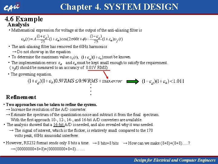
Chapter 4. SYSTEM DESIGN 4. 6 Example Analysis • Mathematical expression for voltage at the output of the anti-aliasing filter is • The anti-aliasing filter has removed the 60 Hz harmonics → Do not show up in the equation • To determine the maximum value must be known. • The implementation errors εd and εa must be kept small enough to satisfy the requirement. ( υf(t) should be measured to an accuracy of 0. 01 V RMS) • The governing equation. Refinement • Two approaches can be taken to refine the system. → Increase the resolution of the A/D converter. → Estimate the spectrum of the quantization noise and subtract it from the final spectrum. With the first approach 10 -, 12 -, 14 -, and 16 -bit A/D converters are available. • The analysis showed that a 16 -bit A/D is needed, and also revealed why it was needed. → The signal of interest, which is the flicker, is relatively small compared to the 170 volts peak, 60 Hz sinusoidal interferer. • However, RS 232 format sends only 8 bits a time. → 8 bits+8 bits → (0000+8+8)+(0000+8+8)……. → How can we make (8+8)+(8+8)…. . ? Design for Electrical and Computer Engineers

Chapter 4. SYSTEM DESIGN • 16 -bit A/D is expensive. → How about using 8 bit A/D and 60 Hz notch filter? → Inductors and capacitors for 60 Hz notch filter would be too large and expensive. → 16 bit A/D is an answer! • But, 60 Hz noise should be suppressed for high accuracy. The design engineer needs → Novel way of suppressing the 60 Hz sinusoid. → This requires a new concept developed with creative thinking. • One novel concept is; → Set the sampling rate to 120 Hz and synchronize the sampling to the zero crossings of the 60 Hz sinusoid. → The 60 Hz interferer is effectively eliminated, as the interferer is zero volts at every sample time. • Such a system → Require a simple clipping circuit to prevent the input to the A/D converter from exceeding limits. → Required a phase-locked loop to lock the sampling clock to the zero crossings of the 60 Hz sinusoid. (for synchronizing) Analysis Refinement Design for Electrical and Computer Engineers

Chapter 4. SYSTEM DESIGN Synthesis/Analysis cycle that we followed is Performance or cost threshold 4. 7 Summary • Conceptualization, synthesis, and analysis → Create an orderly sequence of structures (block diagrams). • Many of the ideas used in synthesis are born while performing the analysis. Two type of thinking • Linear thinking → Logical, deductive reasoning. Used to expand or adapt an existing solution to fit problem. → Linear approach is sometimes the obvious choice. • Creative thinking → deeper and less constrained, searching the imagination for a novel solution. → personal improvement and the potential for revolutionary results • System engineers must act responsibly, be aware of cost and time constraints, and work to ensure the profitability of their firm! Design for Electrical and Computer Engineers