CHAPTER 4 PART 1 INTERCONNECTION IN IC ASSEMBLY
CHAPTER 4 PART 1 INTERCONNECTION IN IC ASSEMBLY DMT 243 PACKAGING ELECTRONICS
CONTENTS § § Level of Interconnection. Wire Bonding. Tape Automated Bonding (TAB). Flip Chip.
INTRODUCTION TO IC ASSEMBLY § IC assembly definition : § Process of electrically connecting I/O bond pads on the IC to the corresponding bond pads on the packages. § First processing step after wafer fabrication and singulation that enables ICs to be packaged for systems use. § The packages included single chip package, multichip package, system level board. § IC assembly process involves 3 interfaces : 1. Metallurgical bond pad interface on the packages. 2. Electrical interconnection between these two interfaces. 3. Metallurgical bond pad interface on the IC.
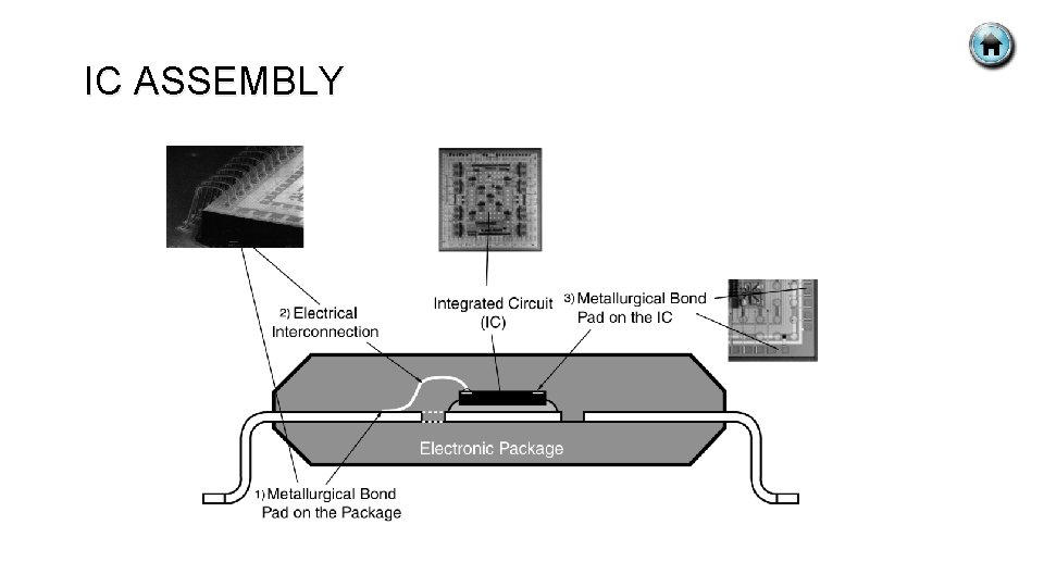
IC ASSEMBLY
PURPOSES OF IC ASSEMBLY § Enable an IC to be electrically interconnected to the package, and to allow that IC to be handled, tested and “burnt-in”. § Such “qualified” IC used in electronic product. § Interconnected to other ICs, passives, flat panel displays, keyboards, sensors, connectors, antennas, switches, etc. § PRIMARY purposes of IC assembly : § To provide signal and power distribution of the packaged IC to the system. § To provide mechanical support to fragile IC. § To provide environmental protection of the IC. § Dissipate heat generated by IC chips. § Facilitate the packaging and handling of IC chips.
REQUIREMENTS OF IC ASSEMBLY § To provide acceptable electrical properties such as capacitance resistance, and inductance. (wirebonding have long lengths resulting in high impedance and longer signal delay times). § IC assembly technologies should provide a low cost solution for the electrical interface between the chip and packages. § High throughput manufacturing. § High reliability. (Flip chip on ceramic technology has been a highly reliable interconnection technique). § Repairability where the interconnection between the IC and the package should provide replacement with a new high quality IC.
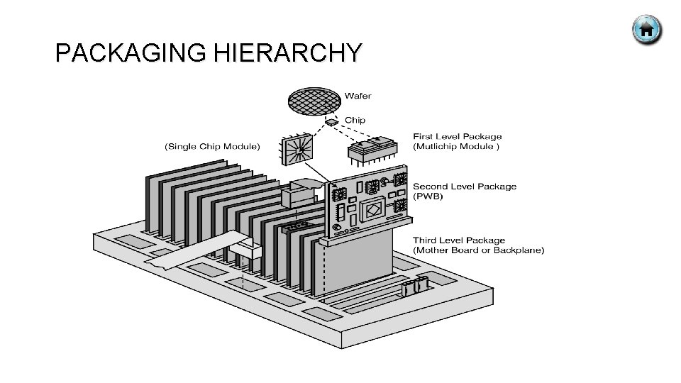
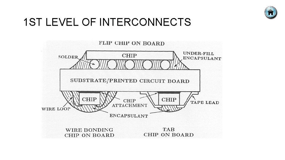
LEVEL OF INTERCONNECTS § Six levels of interconnects : § Level 1 : Chip pad to package leads, e. G. , Wire bonds. § Level 2 : Components to circuit board, e. G. , PLCC socket. § Level 3 : Circuit board (board-to-board) connector, e. G. , Edgeboard connection. § Level 4 : Subassembly interconnects, e. G. , Ribbon cables. § Level 5 : Subassembly to i/o, e. G. , BNC connector. § Level 6 : System interconnects, e. G. , Ethernet connectors.
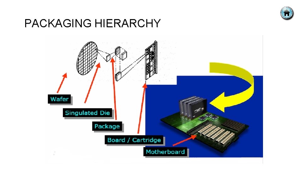
PACKAGING HIERARCHY
PACKAGING HIERARCHY
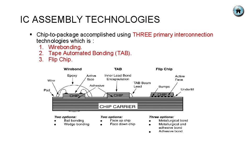
IC ASSEMBLY TECHNOLOGIES § Chip-to-package accomplished using THREE primary interconnection technologies which is : 1. Wirebonding. 2. Tape Automated Bonding (TAB). 3. Flip Chip.
1 ST LEVEL OF INTERCONNECTS
WIREBONDING Wafer Backgrinding Die Preparation Die Attach WIRE BONDING Die Overcoat Electrical Testing DTFS Lead Finish Marking Sealing Molding Tape & Reel Dry Packing Boxing & Labelling
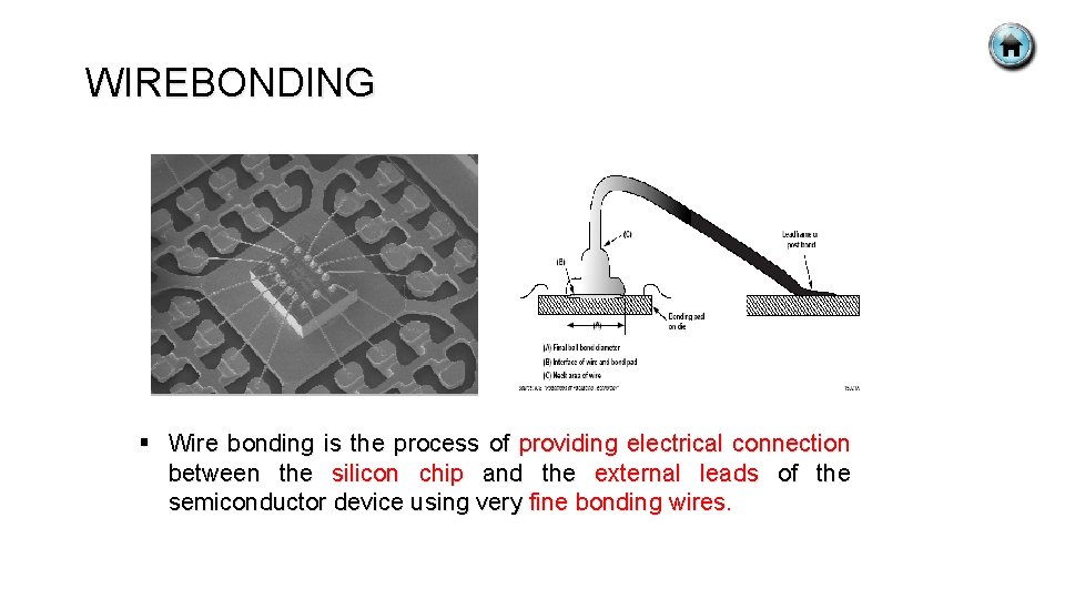
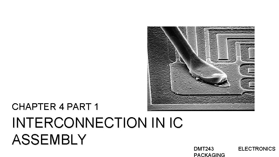
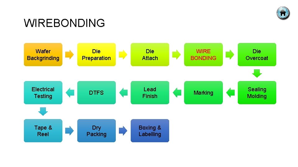
WIREBONDING § Wire bonding is the process of providing electrical connection between the silicon chip and the external leads of the semiconductor device using very fine bonding wires.
WIREBONDING § Technology is originated with AT&T’s beam lead bonding in 1950 s. § Chip-to-package interconnection technique where fine metal is attached between each of the I/O pads on the chip, one at the time. § Two major types of wirebonding : § Gold ball to wedge bonding. § Aluminum wedge to wedge bonding. § Focus on ball bonding, since it dominates this technology. § Gold wire (25µm thickness) is bonded using thermosonic bonding between the IC bond pad and the matching package pad. § Well over 90% of all chip-to-package interconnections formed in 1999.
ADVANTAGES/DISADVANTAGES OF WIREBONDING § Advantages : § Highly flexible chip-to-package interconnection process. § Low defect rates or high yields interconnection processing (40 -1000 ppm). § Easily program or taught bonding cycles. § High reliability interconnection structures. § Very large industry infrastructure supporting the technology. § Rapid advance in equipment, tools and material technology. § Disadvantages : § Slower interconnection rates due point-to-point processing of each wirebonding. § Long chip-to-package interconnection lengths, degrading electrical performances. § Larger footprint (bond pad) required for chip to package interconnect. § Potential for wire sweep during encapsulation overmolding.
WIREBONDING § Ball Bonding : § The most common technique (over 95%) § Wedge Bonding : § The finest pitch bonding capabilities, because the fact that the bonds can be formed by deforming the wire only 25 -30% beyond the original diameter. § Fundamentals of ultrasonic bonding : § Theory states that ultrasonic energy allows the materials to plastically deform at much lower stress compared to pure thermal or mechanical energy. § Materials used in wirebonding : § Gold for ball bonding and aluminum for wedge bonding. § Typical wire diameter is 25µm.
IC/PACKAGES BOND PAD INTERFACES § IC bond pad interfaces : § Al is predominant IC bond pad interface for wire bond interconnect. However, Cu metallization is gaining interest due to increase of performances. § Packages bond pad interfaces : § Metallized leadframes : § Most common material are Cu alloys (e. g Cu-Fe, Cu-Cr, Cu-Ni. Si and Cu-Sn) and some instance Fe-Ni or Fe-Ni-Co alloys are also used. § Lastly at final it will plated/coated with Ni, Au or Sn. § Metallized chip carrier and PWB : § Most common conductor is Cu which is plated with Ni and soft or immersion gold for good solderability.
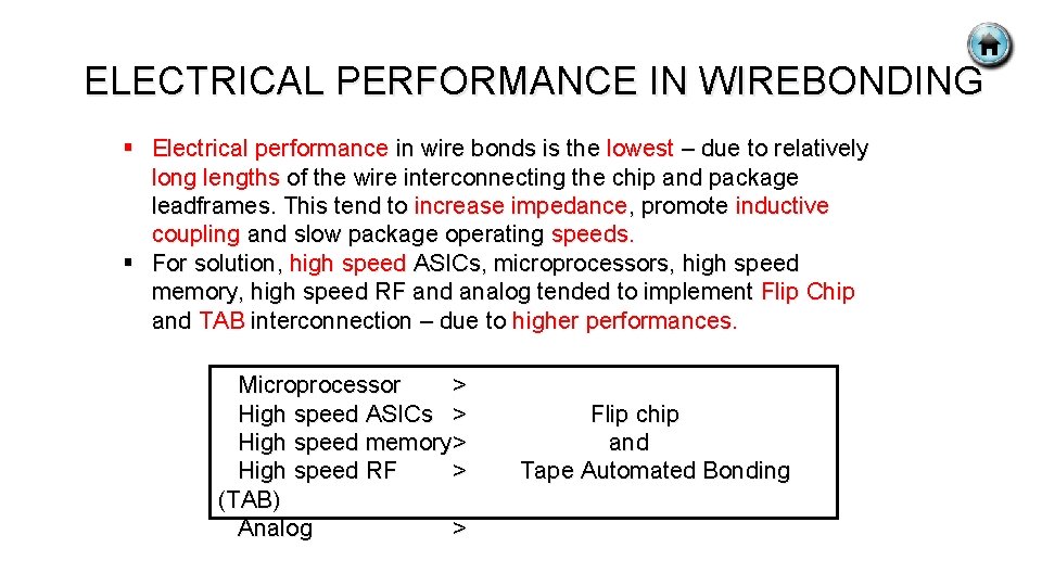
ELECTRICAL PERFORMANCE IN WIREBONDING § Electrical performance in wire bonds is the lowest – due to relatively long lengths of the wire interconnecting the chip and package leadframes. This tend to increase impedance, promote inductive coupling and slow package operating speeds. § For solution, high speed ASICs, microprocessors, high speed memory, high speed RF and analog tended to implement Flip Chip and TAB interconnection – due to higher performances. Microprocessor > High speed ASICs > High speed memory > High speed RF > (TAB) Analog > Flip chip and Tape Automated Bonding
IMPORTANT PARAMETER IN WIREBONDING § Bonding temperature : § Thermal energy is required to 'soften' the harder metal (aluminum) to match their hardness especially if the bond and bond pad are composed of different metals, such as in the case of gold ball/aluminum bond pad bonding. § Au-Al ball bonding generally takes place at 200 -240 deg C. § In cases where the wire and bond pad have similar metallurgies, bonding may occur at ambient temperature, such as in the case of aluminum wedge/aluminum bond pad bonding. § Bonding time : § Optimum time provide good interconnection. Longer time would cause excessive force being applied to the die.
IMPORTANT PARAMETER IN WIREBONDING § Bonding pressure : § Pressure is to keep the bonding tool in control as it scrubs the bond against the bond pad. § Without pressure, the bonding tool would bounce around the bond pad as it receives and transmits the ultrasonic energy. § Ultrasonic energy : § Cleans the bond pad of debris and oxides, exposing a fresh surface of the bond pad. § It also further enhances the metallurgical bond or weld between the bond and the bond pad.
WIREBONDING FAILURE MECHANISMS § Ball bond lifting : § Detachment of the ball bond from the silicon chip; also refers to non-sticking of the ball bond to the bond pad. § Common causes : § Contamination on the bond pad. § Incorrect wirebonding parameter settings. § Instability of the die during bonding. § Bond pad corrosion. § Excessive bond pad probing. § Kirkendall voiding. § Excessive thermal stress resulting in excessive intermetallic formation. § Bond pad metallization/barrier metallization lifting. § Cratering.
WIREBONDING FAILURE MECHANISMS § Wedge bond lifting : § Detachment of the wedge bond from the silicon chip, bonding post, or leadfinger; non-sticking of the wedge bond to the bond pad, post, or leadfinger. § Common causes : § Contamination on the bond pad or leadfinger. § Incorrect parameter settings. § Instability of the die or leadframe during bonding. § Bond pad or leadfinger corrosion. § Excessive bond pad probing.
WIREBONDING FAILURE MECHANISMS § Ball bond neck break : § Breakage of the wire at the neck of the Au ball bond. § Common causes : § Incorrect wirebonding parameter settings, incorrect wire looping, die-to-package delamination, excessive wire sweeping during mold, excessive die overcoat, 'bamboo' grain structure due to excessive thermal treatment. § Midspan wire break : § Breakage along the span of the wire. § Common causes : § Wire nicks or damage, wire corrosion, tight wire looping, excessive wire sweeping, electrical overstress.
WIREBONDING FAILURE MECHANISMS § Bond-to-metal shorting : § Electrical shorting between the bond a metal line on the die. § Common causes : § Incorrect wirebonding parameter settings, incorrect bond placement, insufficient bond pad-to-metal distances. § Bond-to-bond shorting : § Electrical shorting between two bonds. § Common causes : § incorrect wirebond parameter settings, incorrect bond placement, insufficient bond pad-to-bond pad distance. § Wedge bond heel break : § Breakage of the wire at the heel of the Al wedge bond. § Common causes : § Incorrect wirebond parameter settings, incorrect wire looping, leadfinger-to-package delamination.
WIREBONDING FAILURE MECHANISMS § Wire to wire shorting : § Electrical shorting between two wires. § Common causes : § Incorrect wire looping, excessive wiresweeping, insufficient wire-to-wire distance. § Cratering : § Silicon damage under the bond pad, the worst of which is when a chunk of silicon is completely detached from the active circuit. § Common causes : § Incorrect wirebond parameter settings, excessive bond pad probing.
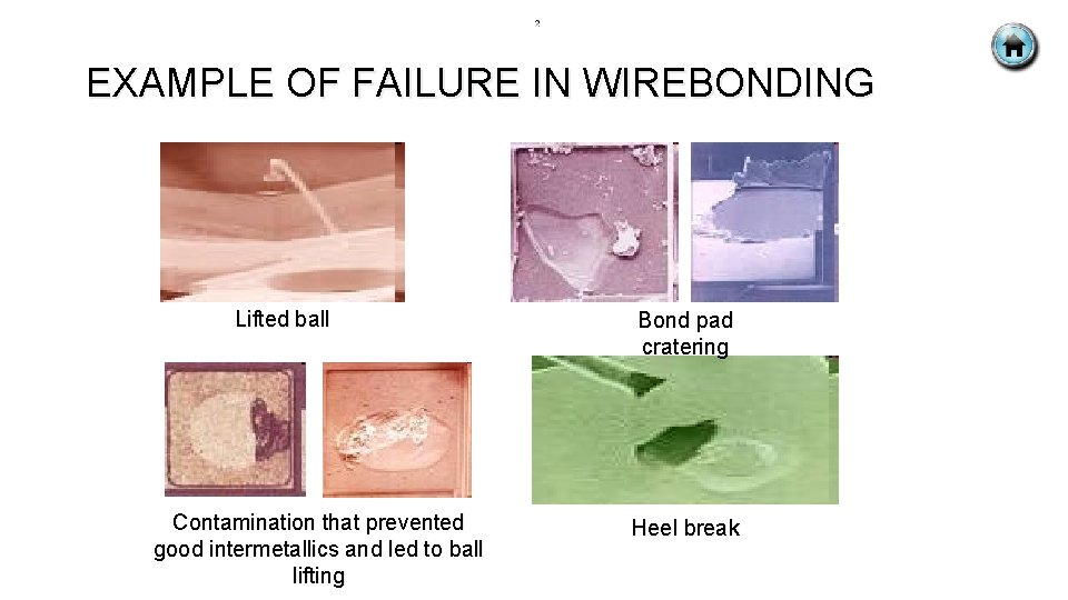
EXAMPLE OF FAILURE IN WIREBONDING Lifted ball Contamination that prevented good intermetallics and led to ball lifting Bond pad cratering Heel break
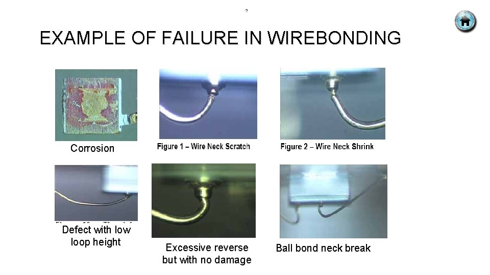
EXAMPLE OF FAILURE IN WIREBONDING Corrosion Defect with low loop height Excessive reverse but with no damage Ball bond neck break
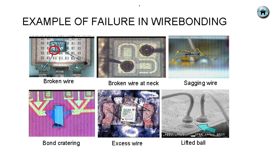
EXAMPLE OF FAILURE IN WIREBONDING Broken wire Bond cratering Broken wire at neck Excess wire Sagging wire Lifted ball
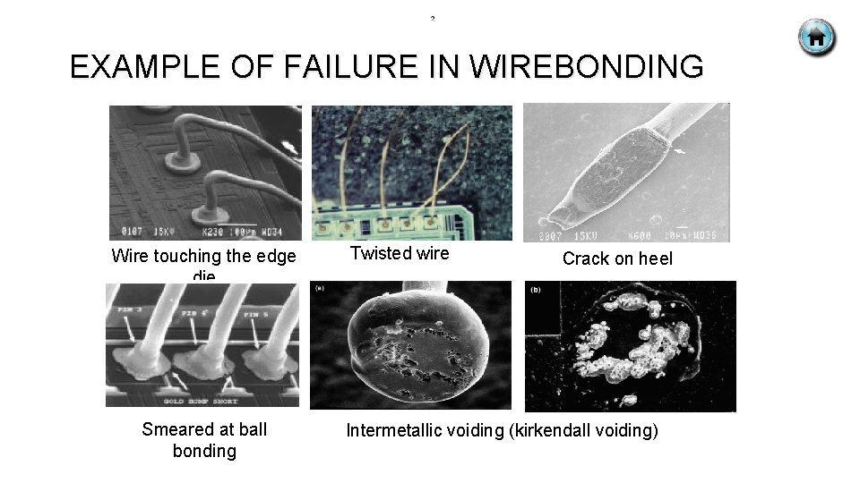
EXAMPLE OF FAILURE IN WIREBONDING Wire touching the edge die Smeared at ball bonding Twisted wire Crack on heel Intermetallic voiding (kirkendall voiding)
- Slides: 29