Chapter 4 Memory Design SOC and BoardBased Systems
Chapter 4 Memory Design: SOC and Board-Based Systems Computer System Design System-on-Chip by M. Flynn & W. Luk Pub. Wiley 2011 (copyright 2011) soc 4. 1
Cache and Memory • cache – performance – cache partitioning – multi-level cache • memory – off-die memory designs soc 4. 2

Outline for memory design soc 4. 3
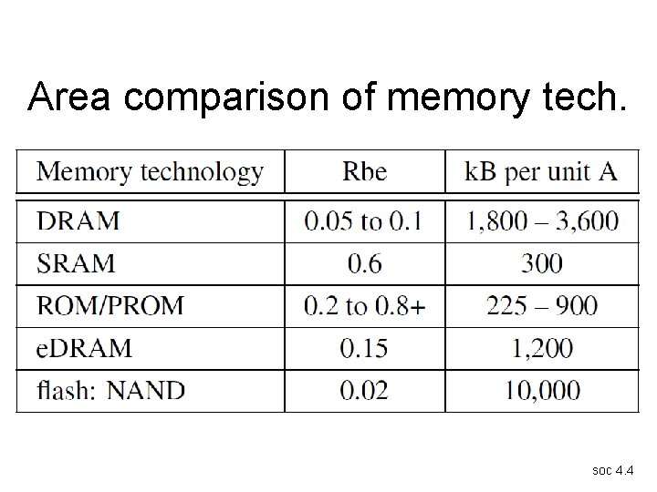
Area comparison of memory tech. soc 4. 4
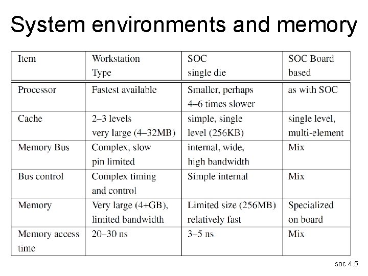
System environments and memory soc 4. 5
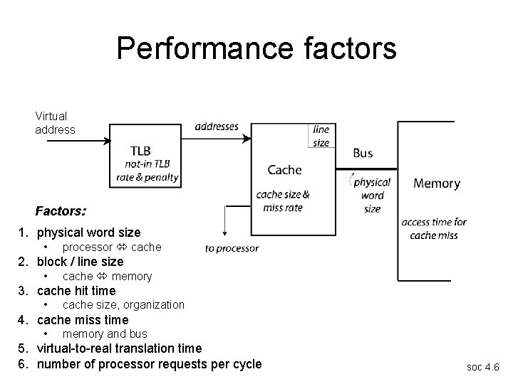
Performance factors Virtual address Factors: 1. physical word size • processor cache 2. block / line size • cache memory 3. cache hit time • cache size, organization 4. cache miss time • memory and bus 5. virtual-to-real translation time 6. number of processor requests per cycle soc 4. 6
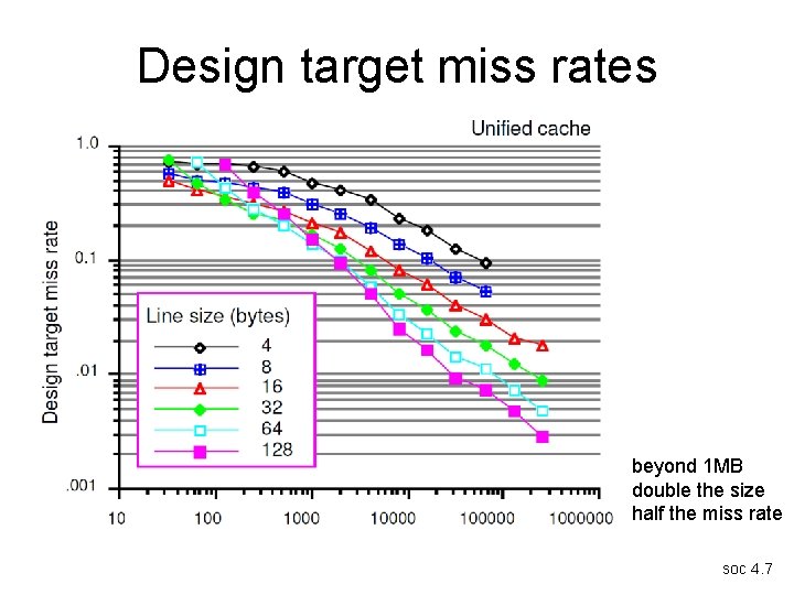
Design target miss rates beyond 1 MB double the size half the miss rate soc 4. 7
System effects limit hit rate • operating System affects the miss ratio – about 20% increase • so does multiprogramming (M) – miss rates may not be affected by increased cache size – Q = no. instructions between task switches soc 4. 8
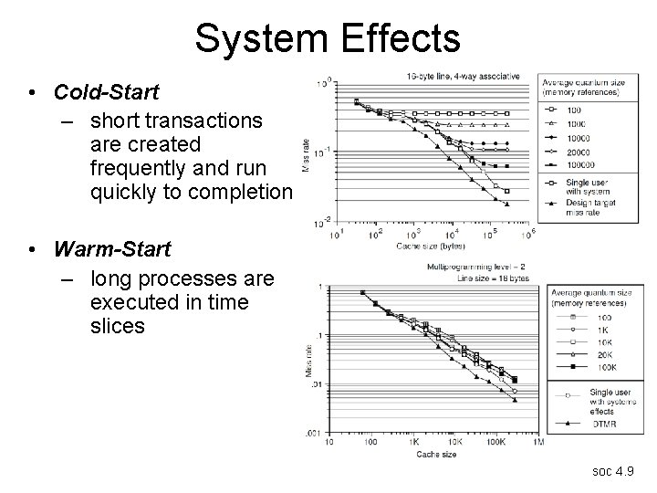
System Effects • Cold-Start – short transactions are created frequently and run quickly to completion • Warm-Start – long processes are executed in time slices COLD soc 4. 9
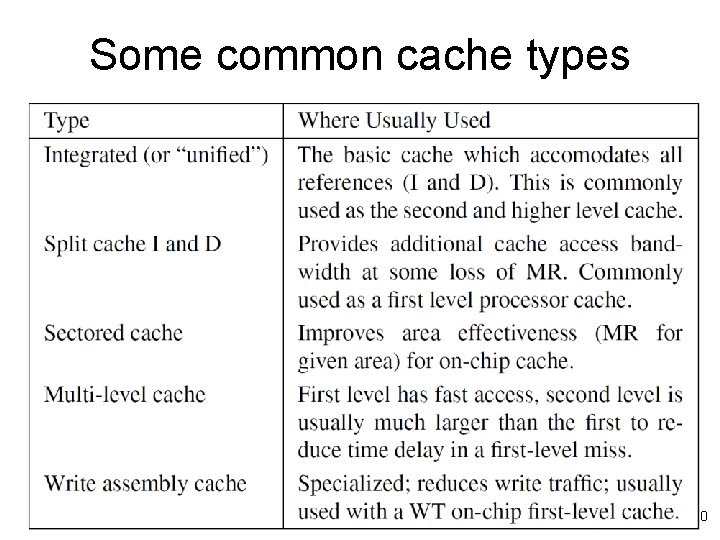
Some common cache types soc 4. 10
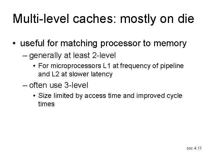
Multi-level caches: mostly on die • useful for matching processor to memory – generally at least 2 -level • For microprocessors L 1 at frequency of pipeline and L 2 at slower latency – often use 3 -level • Size limited by access time and improved cycle times soc 4. 11
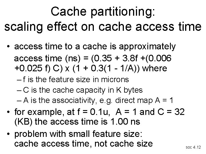
Cache partitioning: scaling effect on cache access time • access time to a cache is approximately access time (ns) = (0. 35 + 3. 8 f +(0. 006 +0. 025 f) C) x (1 + 0. 3(1 - 1/A)) where – f is the feature size in microns – C is the cache capacity in K bytes – A is the associativity, e. g. direct map A = 1 • for example, at f = 0. 1 u, A = 1 and C = 32 (KB) the access time is 1. 00 ns • problem with small feature size: cache access time, not cache size soc 4. 12
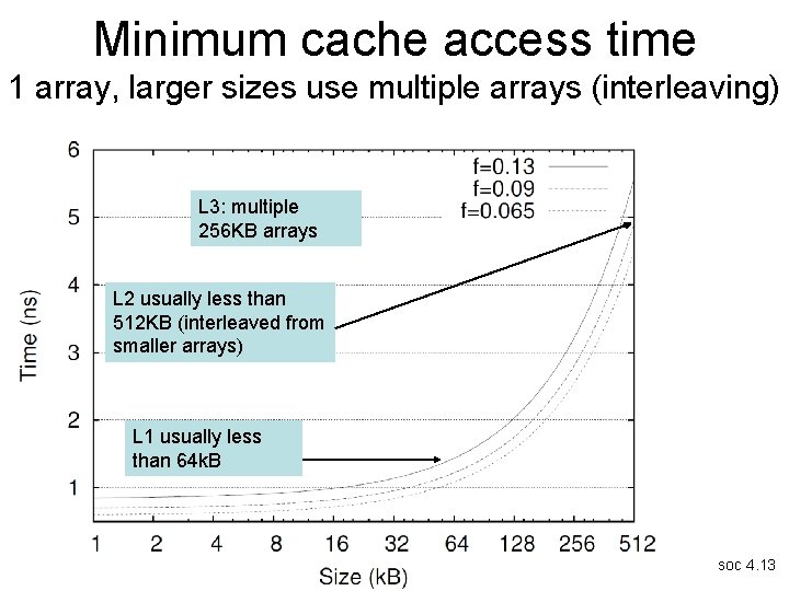
Minimum cache access time 1 array, larger sizes use multiple arrays (interleaving) L 3: multiple 256 KB arrays L 2 usually less than 512 KB (interleaved from smaller arrays) L 1 usually less than 64 k. B soc 4. 13
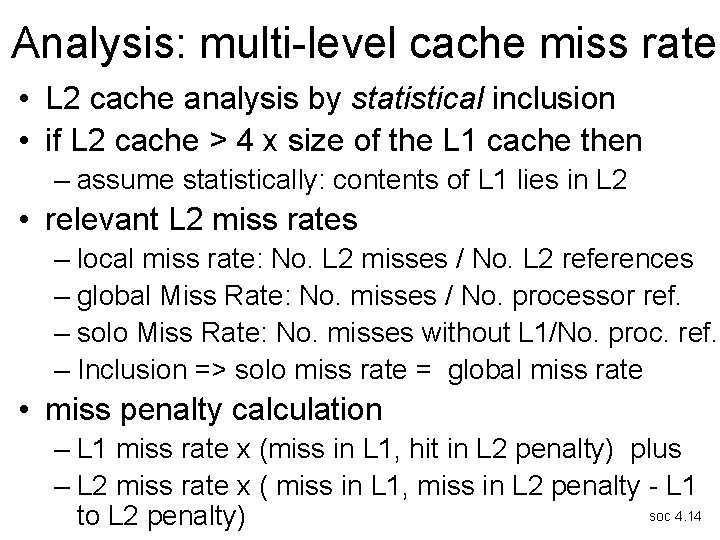
Analysis: multi-level cache miss rate • L 2 cache analysis by statistical inclusion • if L 2 cache > 4 x size of the L 1 cache then – assume statistically: contents of L 1 lies in L 2 • relevant L 2 miss rates – local miss rate: No. L 2 misses / No. L 2 references – global Miss Rate: No. misses / No. processor ref. – solo Miss Rate: No. misses without L 1/No. proc. ref. – Inclusion => solo miss rate = global miss rate • miss penalty calculation – L 1 miss rate x (miss in L 1, hit in L 2 penalty) plus – L 2 miss rate x ( miss in L 1, miss in L 2 penalty - L 1 soc 4. 14 to L 2 penalty)
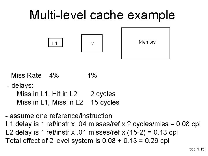
Multi-level cache example L 1 L 2 Memory Miss Rate 4% 1% - delays: Miss in L 1, Hit in L 2 2 cycles Miss in L 1, Miss in L 2 15 cycles - assume one reference/instruction L 1 delay is 1 ref/instr x. 04 misses/ref x 2 cycles/miss = 0. 08 cpi L 2 delay is 1 ref/instr x. 01 misses/ref x (15 -2) = 0. 13 cpi Total effect of 2 level system is 0. 08 + 0. 13 = 0. 29 cpi soc 4. 15
Memory design • • • logical inclusion embedded RAM off-die: DRAM basic memory model Strecker’s model soc 4. 16
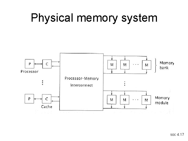
Physical memory system soc 4. 17
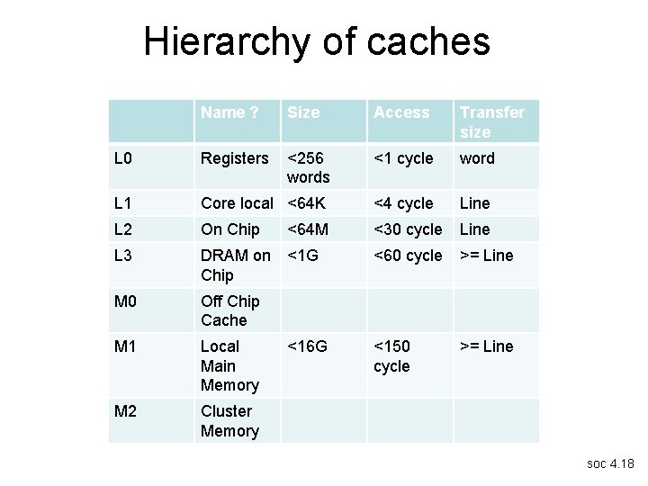
Hierarchy of caches Name ? Size Access Transfer size L 0 Registers <256 words <1 cycle word L 1 Core local <64 K <4 cycle Line L 2 On Chip <64 M <30 cycle Line L 3 DRAM on Chip <1 G <60 cycle >= Line M 0 Off Chip Cache M 1 Local Main Memory <16 G <150 cycle >= Line M 2 Cluster Memory soc 4. 18
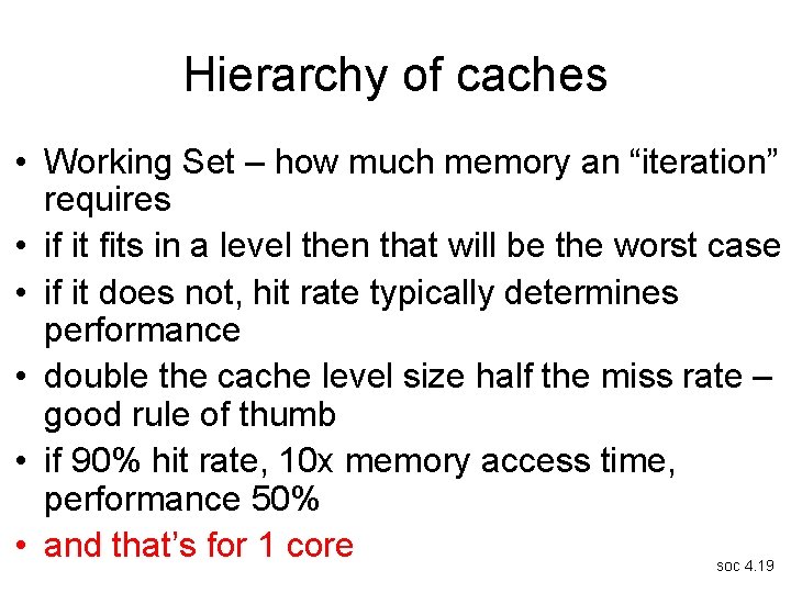
Hierarchy of caches • Working Set – how much memory an “iteration” requires • if it fits in a level then that will be the worst case • if it does not, hit rate typically determines performance • double the cache level size half the miss rate – good rule of thumb • if 90% hit rate, 10 x memory access time, performance 50% • and that’s for 1 core soc 4. 19
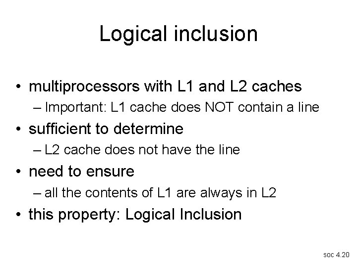
Logical inclusion • multiprocessors with L 1 and L 2 caches – Important: L 1 cache does NOT contain a line • sufficient to determine – L 2 cache does not have the line • need to ensure – all the contents of L 1 are always in L 2 • this property: Logical Inclusion soc 4. 20
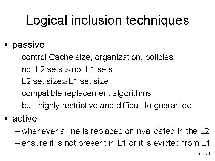
Logical inclusion techniques • passive – control Cache size, organization, policies – no. L 2 sets no. L 1 sets – L 2 set size L 1 set size – compatible replacement algorithms – but: highly restrictive and difficult to guarantee • active – whenever a line is replaced or invalidated in the L 2 – ensure it is not present in L 1 or it is evicted from L 1 soc 4. 21
Memory system design outline • memory chip technology – on-die or off die • static versus dynamic: – SRAM versus DRAM • access protocol: talking to memory – synchronous vs asynchronous DRAMs • simple memory performance model – Strecker’s model for memory banks soc 4. 22
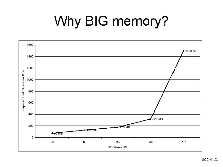
Why BIG memory? soc 4. 23
Memory • many times, computation limited by memory – not processor organization or cycle time • memory: characterized by 3 parameters – size – access time: latency – cycle time: bandwidth soc 4. 24
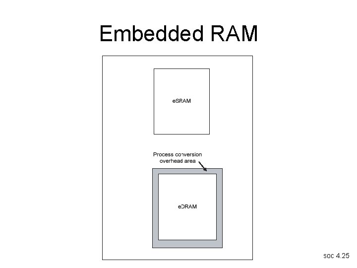
Embedded RAM soc 4. 25

Embedded RAM density (1) soc 4. 26

Embedded RAM density (2) soc 4. 27
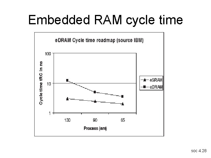
Embedded RAM cycle time soc 4. 28
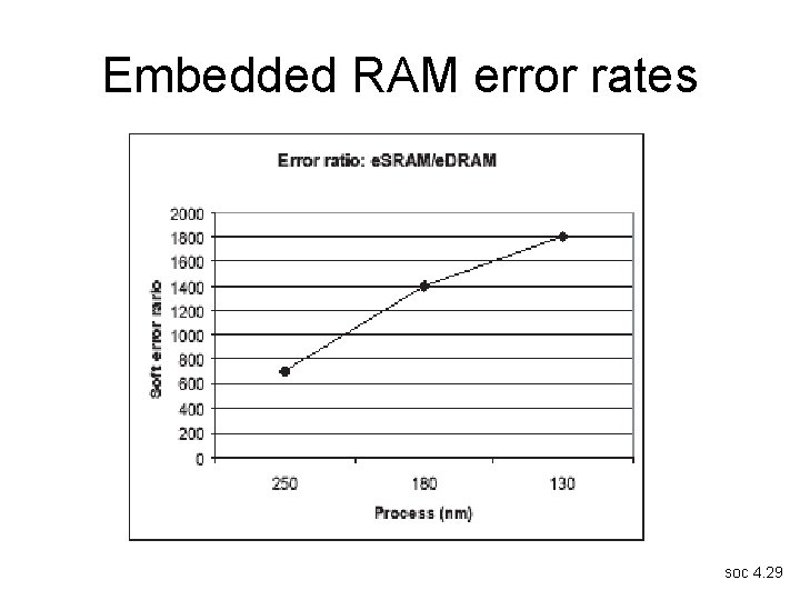
Embedded RAM error rates soc 4. 29
Off-die Memory Module • module contains the DRAM chips that make up the physical memory word • if the DRAM is organized 2 n words x b bits and the memory has p bits/ physical word then the module has p/b DRAM chips. • total memory size is then 2 n words x p bits • Parity or Error-Correction Code (ECC) generally required for error detection and availability soc 4. 30
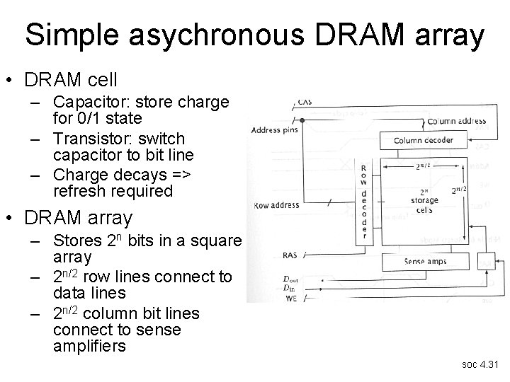
Simple asychronous DRAM array • DRAM cell – Capacitor: store charge for 0/1 state – Transistor: switch capacitor to bit line – Charge decays => refresh required • DRAM array – Stores 2 n bits in a square array – 2 n/2 row lines connect to data lines – 2 n/2 column bit lines connect to sense amplifiers soc 4. 31
DRAM basics • Row read is destructive • Sequence – Read row into SRAM from dynamic memory(>1000 bits) – Select word (<64 bits) – Write Word into row (writing) – Repeat till done with row – WRITE back row into dynamic memory soc 4. 32
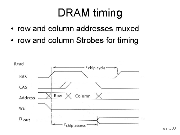
DRAM timing • row and column addresses muxed • row and column Strobes for timing soc 4. 33
Increase DRAM bandwidth • Burst Mode – aka page mode, nibble mode, fast page mode • Synchronous DRAM (SDRAM) • DDR SDRAM – DDR 1 – DDR 2 – DDR 3 soc 4. 34
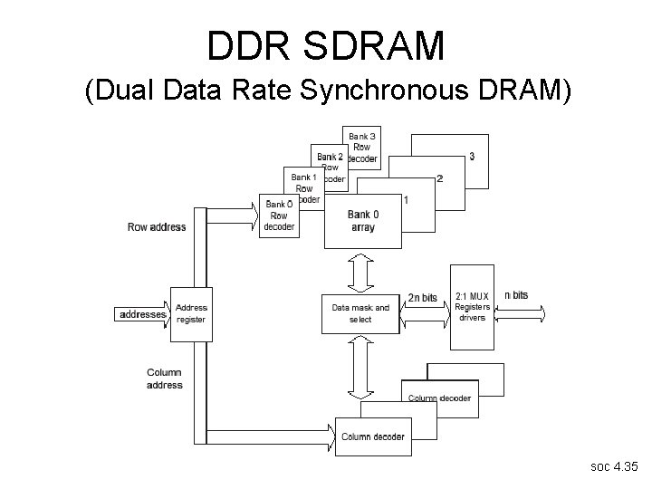
DDR SDRAM (Dual Data Rate Synchronous DRAM) soc 4. 35
Burst mode • burst mode – save most recently accessed row (“page”) – only need column row + CAS to access within page • most DDR SDRAMs: multiple rows can be open – address counter in each row for sequential accesses – only need CAS (DRAM) or bus clock (SDRAM) for sequential accesses soc 4. 36
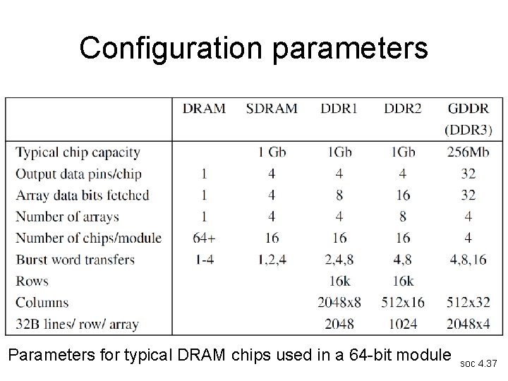
Configuration parameters Parameters for typical DRAM chips used in a 64 -bit module soc 4. 37
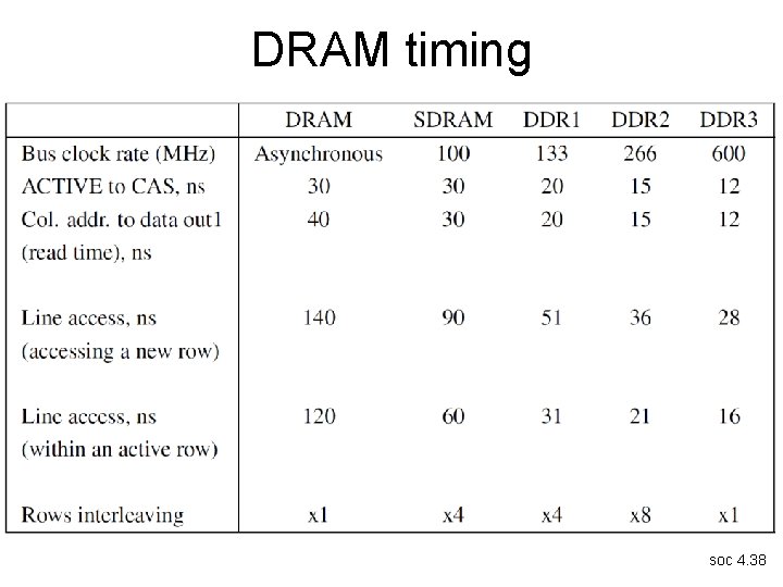
DRAM timing soc 4. 38
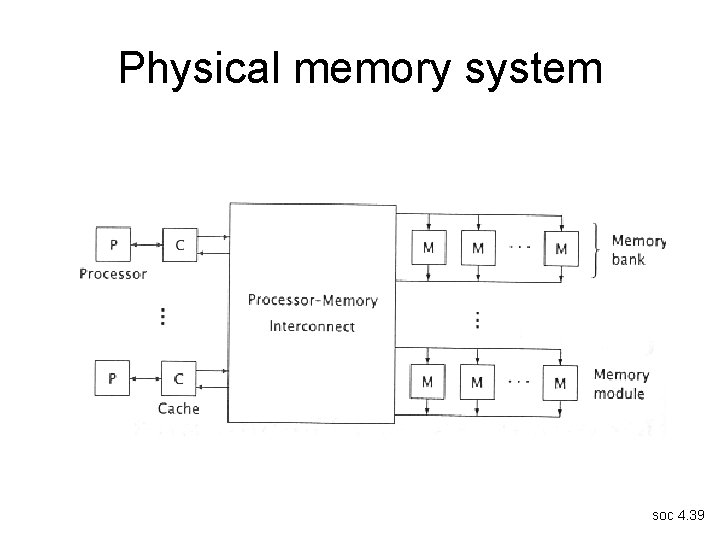
Physical memory system soc 4. 39
Basic memory model • assume that n processors – each make 1 request per Tc to one of m memories • B(n, m) – number of successes • Tc – memory cycle time to the memory • one processor making n requests per Tc – behaves as n processors making 1 request per Tc soc 4. 40
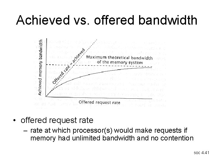
Achieved vs. offered bandwidth • offered request rate – rate at which processor(s) would make requests if memory had unlimited bandwidth and no contention soc 4. 41
Basic terms • B = B(m, n) or B(m) – number of requests that succeed each Tc (= average number of busy modules) – B: bandwidth normalized to Tc • Ts: more generalized term for service time – Tc = Ts • BW: achieved bandwidth – in requests serviced per second – BW = B / Ts = B(m, n)/ Ts soc 4. 42
Modeling + evaluation methodology • relevant physical parameters for memory – word size – module size – number of modules – cycle time Tc (=Ts) • find the offered Bandwidth – number of requests/Ts • find the bottleneck – performance limited by most restrictive service point soc 4. 43
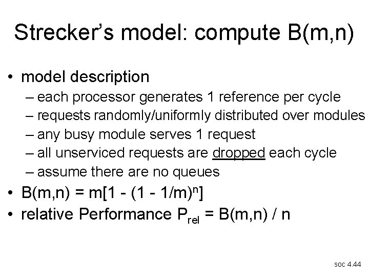
Strecker’s model: compute B(m, n) • model description – each processor generates 1 reference per cycle – requests randomly/uniformly distributed over modules – any busy module serves 1 request – all unserviced requests are dropped each cycle – assume there are no queues • B(m, n) = m[1 - (1 - 1/m)n] • relative Performance Prel = B(m, n) / n soc 4. 44
![Deriving Strecker’s model • Prob[given processor not reference module] = (1 – 1/m) • Deriving Strecker’s model • Prob[given processor not reference module] = (1 – 1/m) •](http://slidetodoc.com/presentation_image_h2/99c8abe5f4fb6be80f13ded8971c05b5/image-45.jpg)
Deriving Strecker’s model • Prob[given processor not reference module] = (1 – 1/m) • Prob[no processor references module] = P[idle] = (1 – 1/m)n • Prob[module busy] = 1 - (1 – 1/m)n • average number of busy modules is B(m, n) • B(m, n) = m[1 - (1 - 1/m)n] soc 4. 45
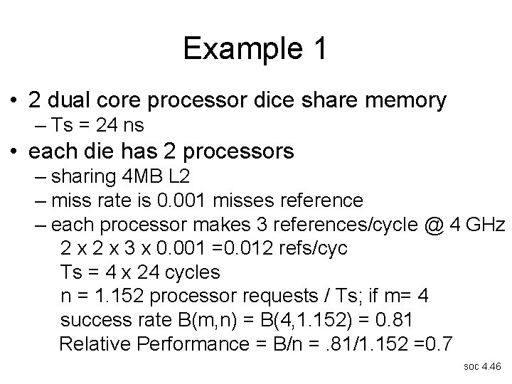
Example 1 • 2 dual core processor dice share memory – Ts = 24 ns • each die has 2 processors – sharing 4 MB L 2 – miss rate is 0. 001 misses reference – each processor makes 3 references/cycle @ 4 GHz 2 x 3 x 0. 001 =0. 012 refs/cyc Ts = 4 x 24 cycles n = 1. 152 processor requests / Ts; if m= 4 success rate B(m, n) = B(4, 1. 152) = 0. 81 Relative Performance = B/n =. 81/1. 152 =0. 7 soc 4. 46
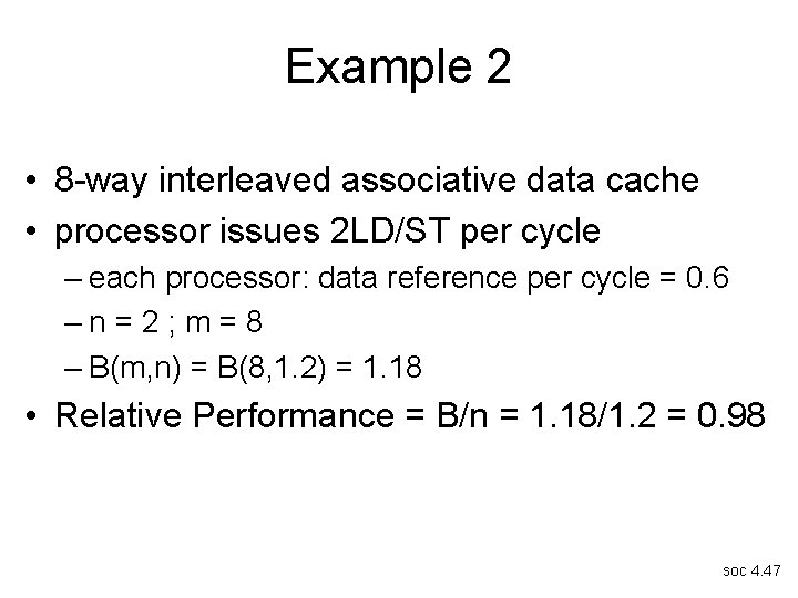
Example 2 • 8 -way interleaved associative data cache • processor issues 2 LD/ST per cycle – each processor: data reference per cycle = 0. 6 –n=2; m=8 – B(m, n) = B(8, 1. 2) = 1. 18 • Relative Performance = B/n = 1. 18/1. 2 = 0. 98 soc 4. 47
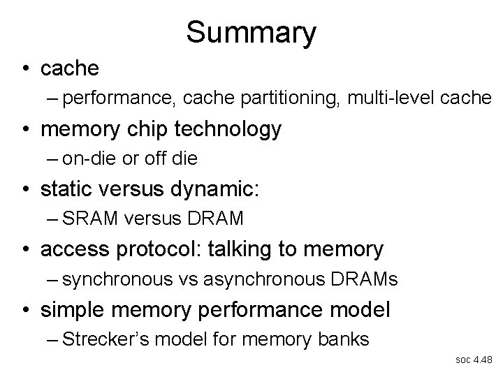
Summary • cache – performance, cache partitioning, multi-level cache • memory chip technology – on-die or off die • static versus dynamic: – SRAM versus DRAM • access protocol: talking to memory – synchronous vs asynchronous DRAMs • simple memory performance model – Strecker’s model for memory banks soc 4. 48
- Slides: 48