Chapter 4 Introduction to Computer Organization 2021 05
- Slides: 31

Chapter 4 Introduction to Computer Organization 2021 -05 -26 1

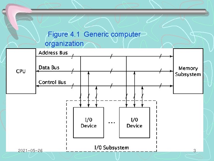
4. 1 Basic Computer Organization Bus (Refer to Figure 4. 1) Address bus Data bus Control bus I/O bus (local bus) 2021 -05 -26 2

Figure 4. 1 Generic computer organization 2021 -05 -26 3

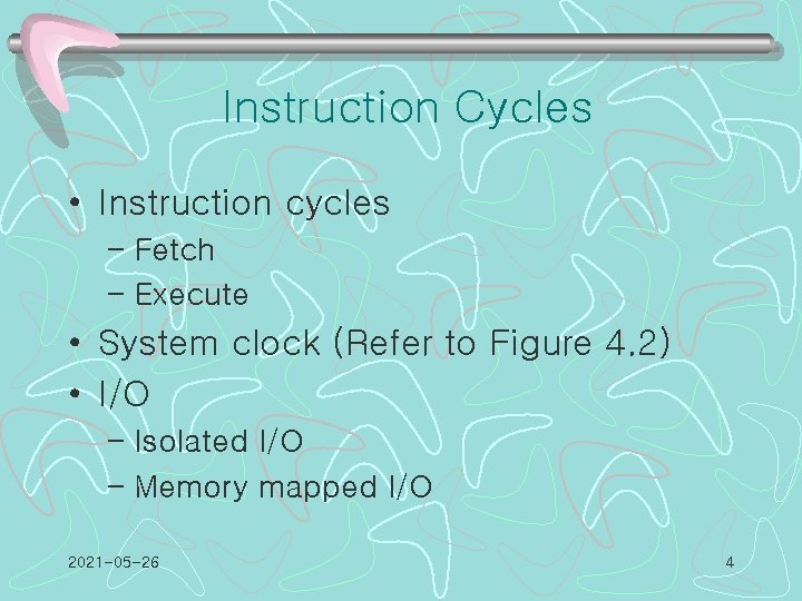
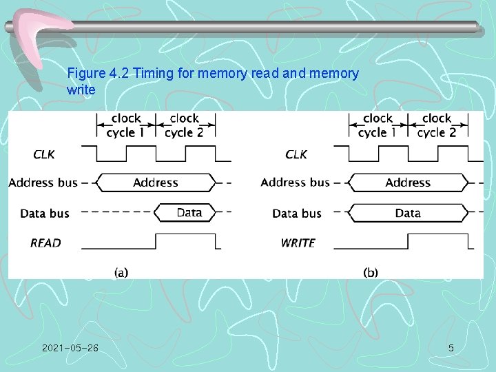
Instruction Cycles • Instruction cycles – Fetch – Execute • System clock (Refer to Figure 4. 2) • I/O – Isolated I/O – Memory mapped I/O 2021 -05 -26 4

Figure 4. 2 Timing for memory read and memory write 2021 -05 -26 5

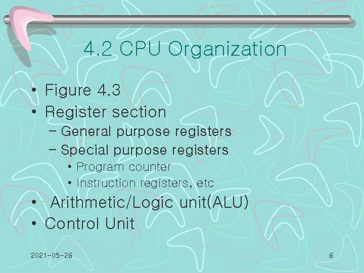
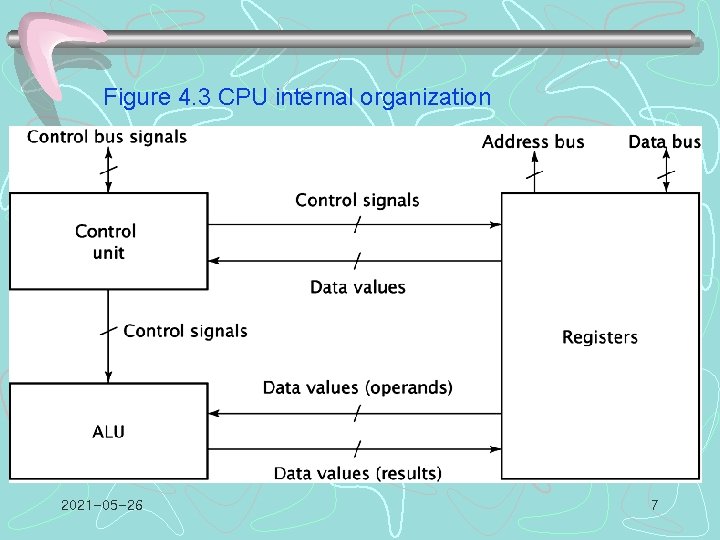
4. 2 CPU Organization • Figure 4. 3 • Register section – General purpose registers – Special purpose registers • Program counter • Instruction registers, etc • Arithmetic/Logic unit(ALU) • Control Unit 2021 -05 -26 6

Figure 4. 3 CPU internal organization 2021 -05 -26 7

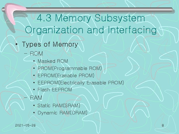
4. 3 Memory Subsystem Organization and Interfacing • Types of Memory – ROM • • • Masked ROM PROM(Programmable ROM) EPROM(Erasable PROM) EEPROM(Electrically Erasable PROM) Flash EEPROM – RAM • Static RAM(SRAM) • Dynamic RAM(DRAM) 2021 -05 -26 8

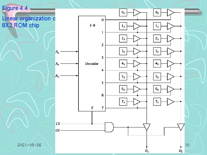
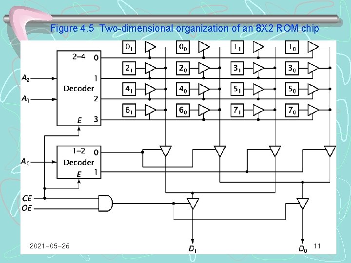
Internal Chip Organization • Linear organization (Figure 4. 4) • Two-dimension organization (Figure 4. 5) 2021 -05 -26 9

Figure 4. 4 Linear organization of an 8 X 2 ROM chip 2021 -05 -26 10

Figure 4. 5 Two-dimensional organization of an 8 X 2 ROM chip 2021 -05 -26 11

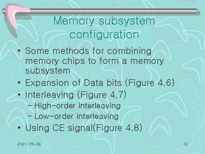
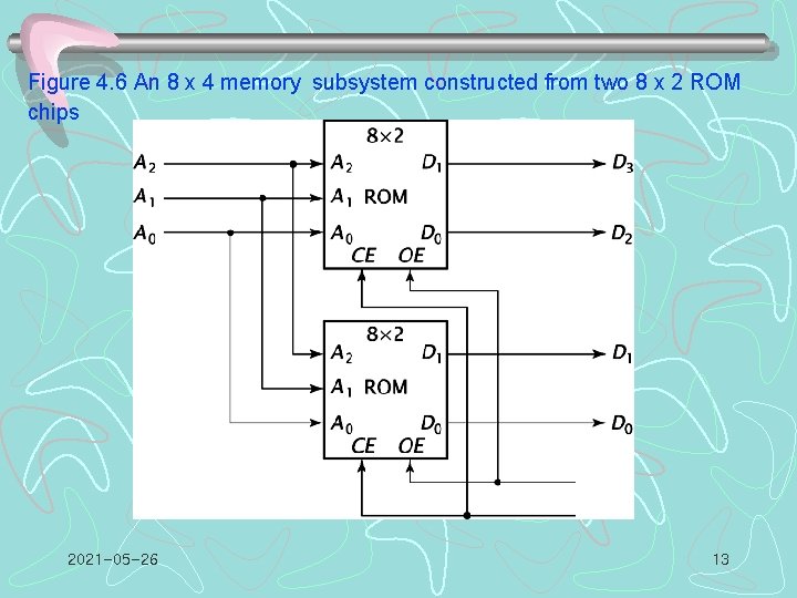
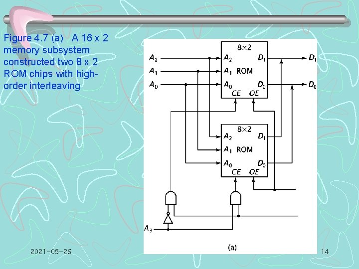
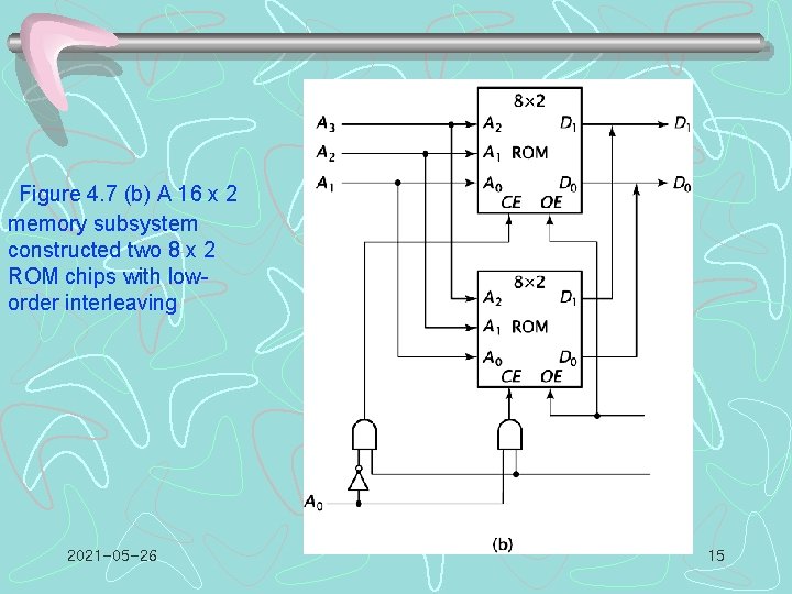
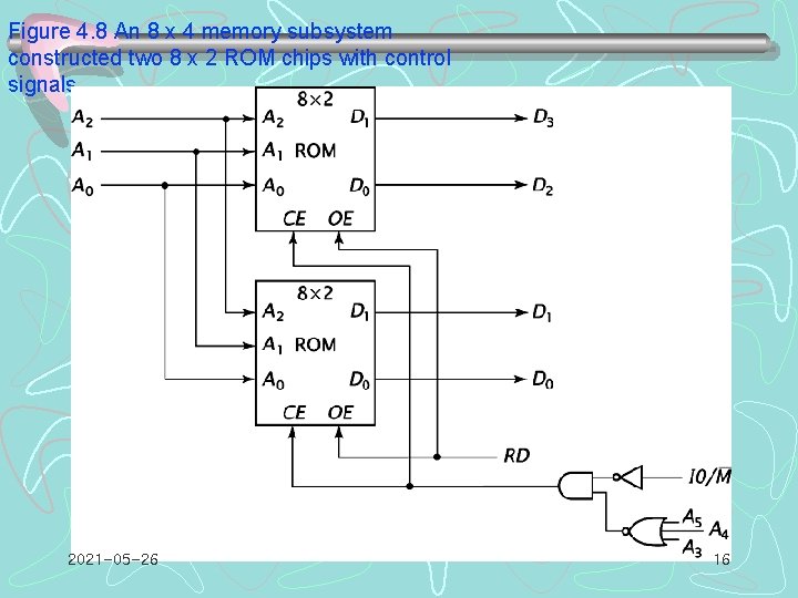
Memory subsystem configuration • Some methods for combining memory chips to form a memory subsystem • Expansion of Data bits (Figure 4. 6) • Interleaving (Figure 4. 7) – High-order interleaving – Low-order interleaving • Using CE signal(Figure 4. 8) 2021 -05 -26 12

Figure 4. 6 An 8 x 4 memory subsystem constructed from two 8 x 2 ROM chips 2021 -05 -26 13

Figure 4. 7 (a) A 16 x 2 memory subsystem constructed two 8 x 2 ROM chips with highorder interleaving 2021 -05 -26 14

Figure 4. 7 (b) A 16 x 2 memory subsystem constructed two 8 x 2 ROM chips with loworder interleaving 2021 -05 -26 15

Figure 4. 8 An 8 x 4 memory subsystem constructed two 8 x 2 ROM chips with control signals 2021 -05 -26 16

Historical perspective • Von Neumann architectures • Harvard architectures 2021 -05 -26 17

Multibyte data organization • Table 3. 1 – Big endian – Little endian • Alignment of multibyte words 2021 -05 -26 18

Beyond the basics • Cache memory • Virtual memory 2021 -05 -26 19

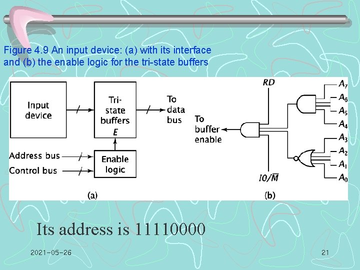
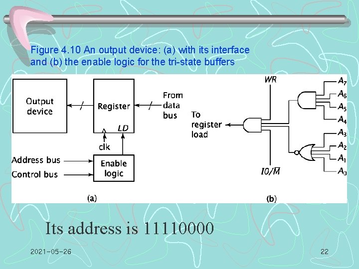
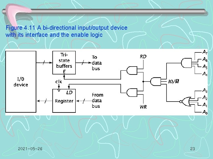
4. 4 I/O Subsystem Organization and Interfacing • Enable logic 2021 -05 -26 20

Figure 4. 9 An input device: (a) with its interface and (b) the enable logic for the tri-state buffers Its address is 11110000 2021 -05 -26 21

Figure 4. 10 An output device: (a) with its interface and (b) the enable logic for the tri-state buffers Its address is 11110000 2021 -05 -26 22

Figure 4. 11 A bi-directional input/output device with its interface and the enable logic 2021 -05 -26 23

Interrupts and DMA? 2021 -05 -26 24

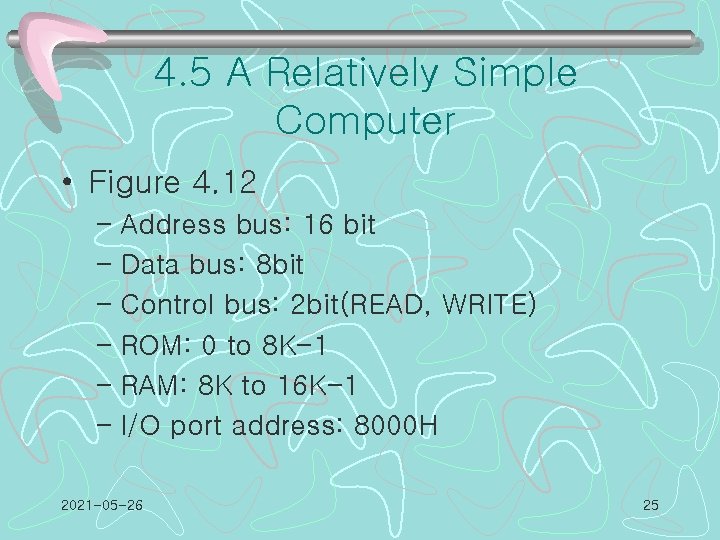
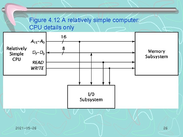
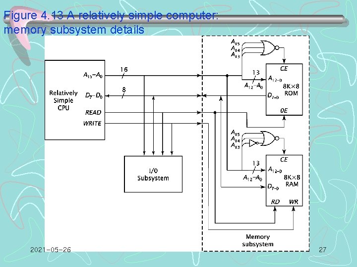
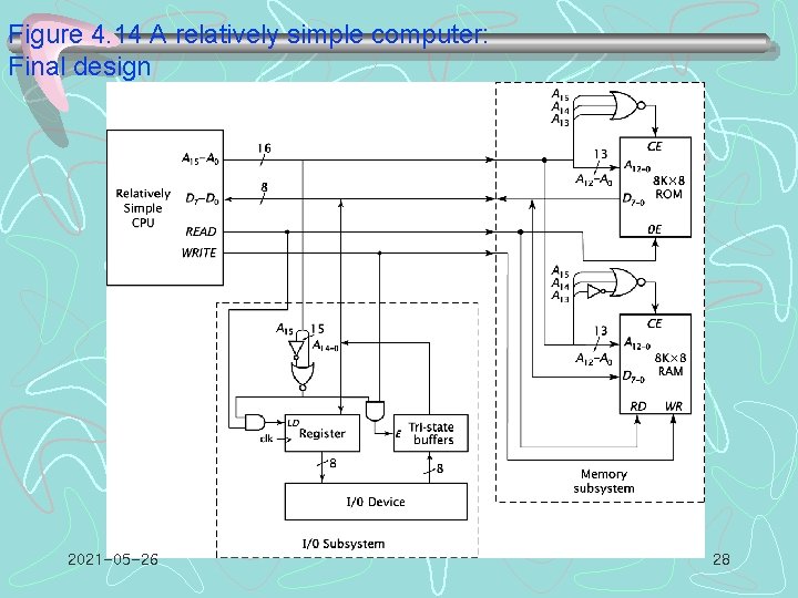
4. 5 A Relatively Simple Computer • Figure 4. 12 – Address bus: 16 bit – Data bus: 8 bit – Control bus: 2 bit(READ, WRITE) – ROM: 0 to 8 K-1 – RAM: 8 K to 16 K-1 – I/O port address: 8000 H 2021 -05 -26 25

Figure 4. 12 A relatively simple computer: CPU details only 2021 -05 -26 26

Figure 4. 13 A relatively simple computer: memory subsystem details 2021 -05 -26 27

Figure 4. 14 A relatively simple computer: Final design 2021 -05 -26 28

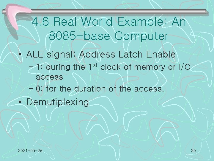
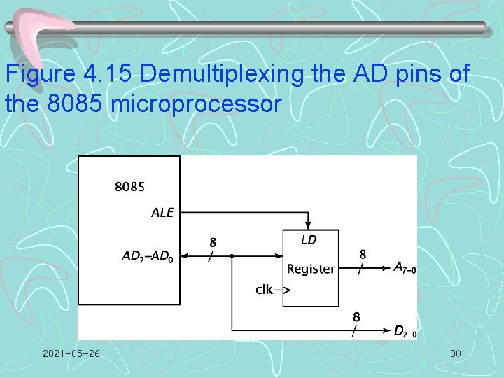
4. 6 Real World Example: An 8085 -base Computer • ALE signal: Address Latch Enable – 1: during the 1 st clock of memory or I/O access – 0: for the duration of the access. • Demutiplexing 2021 -05 -26 29

Figure 4. 15 Demultiplexing the AD pins of the 8085 microprocessor 2021 -05 -26 30

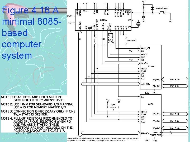
Figure 4. 16 A minimal 8085 based computer system 2021 -05 -26 31