Chapter 4 FieldEffect Transistors Microelectronic Circuit Design Richard
- Slides: 63

Chapter 4 Field-Effect Transistors Microelectronic Circuit Design Richard C. Jaeger Travis N. Blalock Jaeger/Blalock 7/1/03 Microelectronic Circuit Design Mc. Graw-Hill Chap 4 -1

Chapter Goals • Describe operation of MOSFETs and JFETs. • Define FET characteristics in operation regions of cutoff, triode and saturation. • Develop mathematical models for i-v characteristics of MOSFETs and JFETs. • Introduce graphical representations for output and transfer characteristic descriptions of electron devices. • Define and contrast characteristics of enhancement-mode and depletion -mode FETs. • Define symbols to represent FETs in circuit schematics. • Investigate circuits that bias transistors into different operating regions. • Learn basic structure and mask layout for MOS transistors and circuits. • Explore MOS device scaling Jaeger/Blalock 7/1/03 Microelectronic Circuit Design Mc. Graw-Hill Chap 1 -2

Chapter Goals (contd. ) • Contrast 3 and 4 terminal device behavior. • Descibe sources of capacitance in MOSFETs and JFETs. • Explore FET modeling in SPICE. Jaeger/Blalock 7/1/03 Microelectronic Circuit Design Mc. Graw-Hill Chap 1 -3

Types of Field-Effect Transistors • MOSFET (Metal-Oxide Semiconductor Field-Effect Transistor) – Primary componenet in high-density VLSI chips such as memories and microprocessors • JFET (Junction Field-Effect Transistor) – Finds application especially in analog and RF circuit design Jaeger/Blalock 7/1/03 Microelectronic Circuit Design Mc. Graw-Hill Chap 1 -4

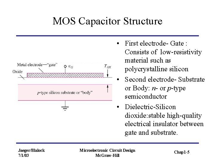
MOS Capacitor Structure • First electrode- Gate : Consists of low-resistivity material such as polycrystalline silicon • Second electrode- Substrate or Body: n- or p-type semiconductor • Dielectric-Silicon dioxide: stable high-quality electrical insulator between gate and substrate. Jaeger/Blalock 7/1/03 Microelectronic Circuit Design Mc. Graw-Hill Chap 1 -5

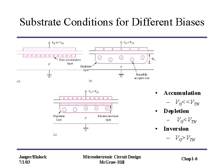
Substrate Conditions for Different Biases • Accumulation – VG<<VTN • Depletion – VG<VTN • Inversion – VG>VTN Jaeger/Blalock 7/1/03 Microelectronic Circuit Design Mc. Graw-Hill Chap 1 -6

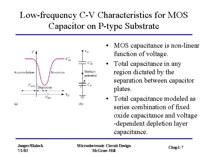
Low-frequency C-V Characteristics for MOS Capacitor on P-type Substrate • MOS capacitance is non-linear function of voltage. • Total capacitance in any region dictated by the separation between capacitor plates. • Total capacitance modeled as series combination of fixed oxide capacitance and voltage -dependent depletion layer capacitance. Jaeger/Blalock 7/1/03 Microelectronic Circuit Design Mc. Graw-Hill Chap 1 -7

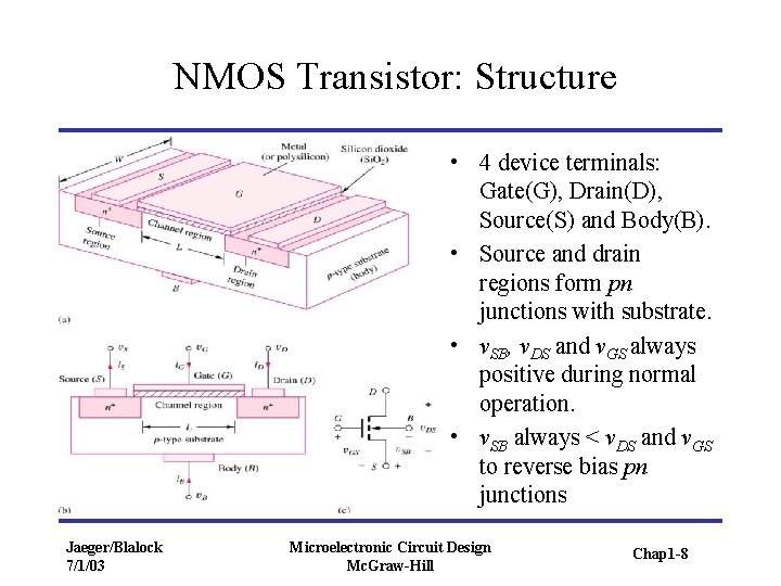
NMOS Transistor: Structure • 4 device terminals: Gate(G), Drain(D), Source(S) and Body(B). • Source and drain regions form pn junctions with substrate. • v. SB, v. DS and v. GS always positive during normal operation. • v. SB always < v. DS and v. GS to reverse bias pn junctions Jaeger/Blalock 7/1/03 Microelectronic Circuit Design Mc. Graw-Hill Chap 1 -8

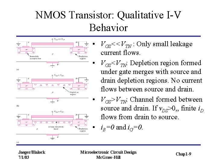
NMOS Transistor: Qualitative I-V Behavior • VGS<<VTN : Only small leakage current flows. • VGS<VTN: Depletion region formed under gate merges with source and drain depletion regions. No current flows between source and drain. • VGS>VTN: Channel formed between source and drain. If v. DS>0, , finite i. D flows from drain to source. • i. B=0 and i. G=0. Jaeger/Blalock 7/1/03 Microelectronic Circuit Design Mc. Graw-Hill Chap 1 -9

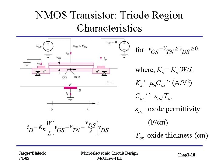
NMOS Transistor: Triode Region Characteristics for where, Kn= Kn’W/L Kn’=μn. Cox’’ (A/V 2) Cox’’=εox/Tox εox=oxide permittivity (F/cm) Tox=oxide thickness (cm) Jaeger/Blalock 7/1/03 Microelectronic Circuit Design Mc. Graw-Hill Chap 1 -10

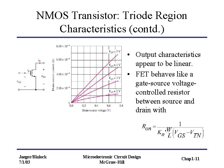
NMOS Transistor: Triode Region Characteristics (contd. ) • Output characteristics appear to be linear. • FET behaves like a gate-source voltagecontrolled resistor between source and drain with Jaeger/Blalock 7/1/03 Microelectronic Circuit Design Mc. Graw-Hill Chap 1 -11

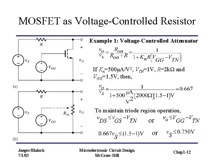
MOSFET as Voltage-Controlled Resistor Example 1: Voltage-Controlled Attenuator If Kn=500μA/V 2, VTN=1 V, R=2 kΩ and VGG=1. 5 V, then, To maintain triode region operation, or or Jaeger/Blalock 7/1/03 Microelectronic Circuit Design Mc. Graw-Hill Chap 1 -12

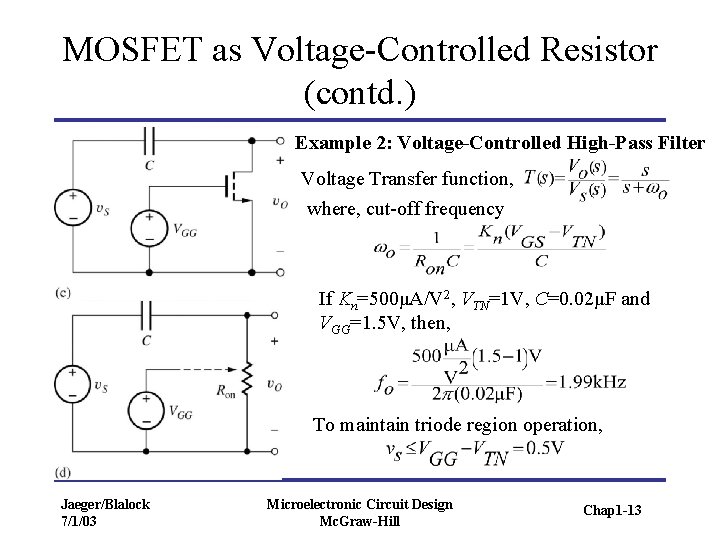
MOSFET as Voltage-Controlled Resistor (contd. ) Example 2: Voltage-Controlled High-Pass Filter Voltage Transfer function, where, cut-off frequency If Kn=500μA/V 2, VTN=1 V, C=0. 02μF and VGG=1. 5 V, then, To maintain triode region operation, Jaeger/Blalock 7/1/03 Microelectronic Circuit Design Mc. Graw-Hill Chap 1 -13

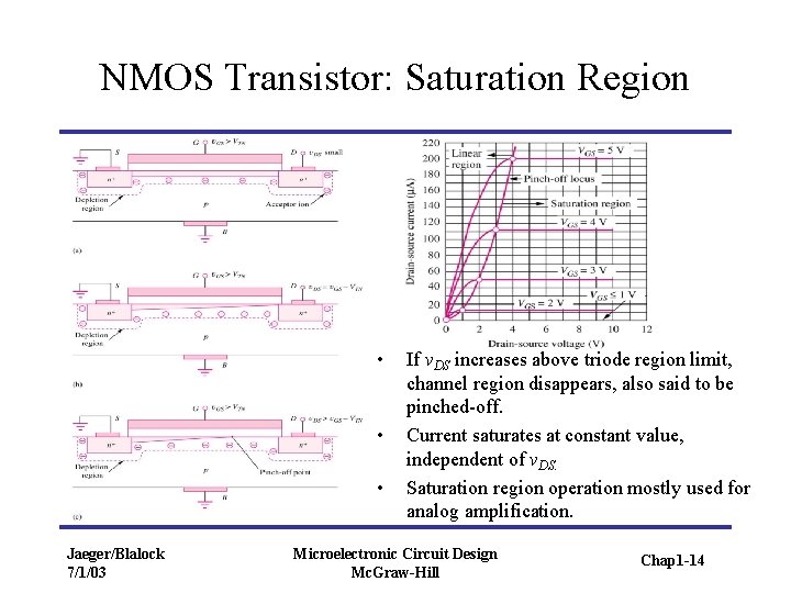
NMOS Transistor: Saturation Region • • • Jaeger/Blalock 7/1/03 If v. DS increases above triode region limit, channel region disappears, also said to be pinched-off. Current saturates at constant value, independent of v. DS. Saturation region operation mostly used for analog amplification. Microelectronic Circuit Design Mc. Graw-Hill Chap 1 -14

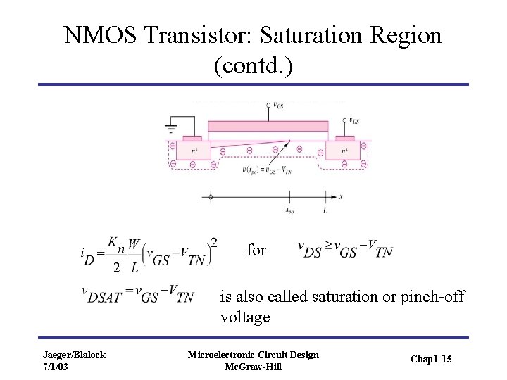
NMOS Transistor: Saturation Region (contd. ) for is also called saturation or pinch-off voltage Jaeger/Blalock 7/1/03 Microelectronic Circuit Design Mc. Graw-Hill Chap 1 -15

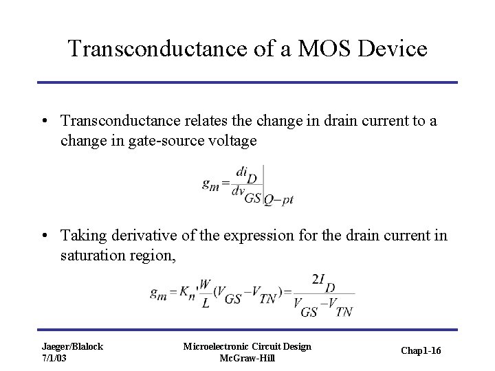
Transconductance of a MOS Device • Transconductance relates the change in drain current to a change in gate-source voltage • Taking derivative of the expression for the drain current in saturation region, Jaeger/Blalock 7/1/03 Microelectronic Circuit Design Mc. Graw-Hill Chap 1 -16

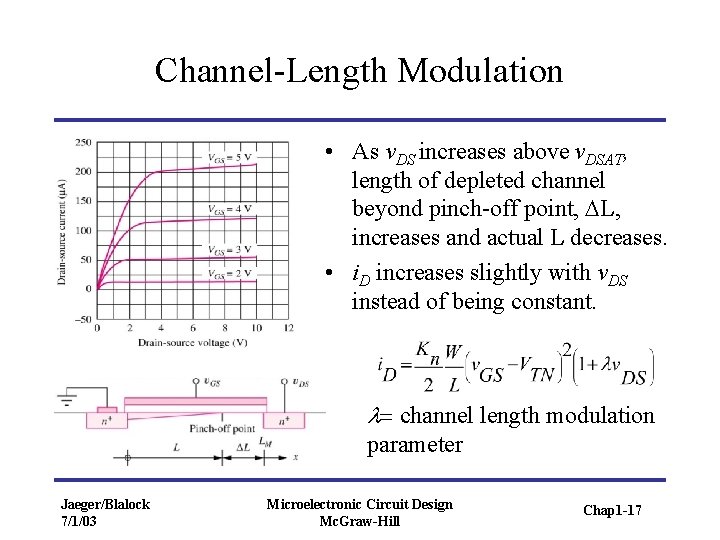
Channel-Length Modulation • As v. DS increases above v. DSAT, length of depleted channel beyond pinch-off point, DL, increases and actual L decreases. • i. D increases slightly with v. DS instead of being constant. l= channel length modulation parameter Jaeger/Blalock 7/1/03 Microelectronic Circuit Design Mc. Graw-Hill Chap 1 -17

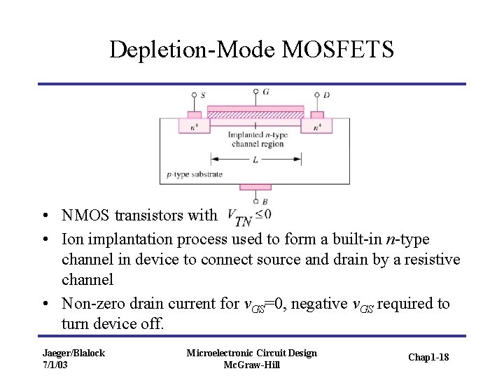
Depletion-Mode MOSFETS • NMOS transistors with • Ion implantation process used to form a built-in n-type channel in device to connect source and drain by a resistive channel • Non-zero drain current for v. GS=0, negative v. GS required to turn device off. Jaeger/Blalock 7/1/03 Microelectronic Circuit Design Mc. Graw-Hill Chap 1 -18

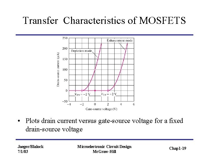
Transfer Characteristics of MOSFETS • Plots drain current versus gate-source voltage for a fixed drain-source voltage Jaeger/Blalock 7/1/03 Microelectronic Circuit Design Mc. Graw-Hill Chap 1 -19

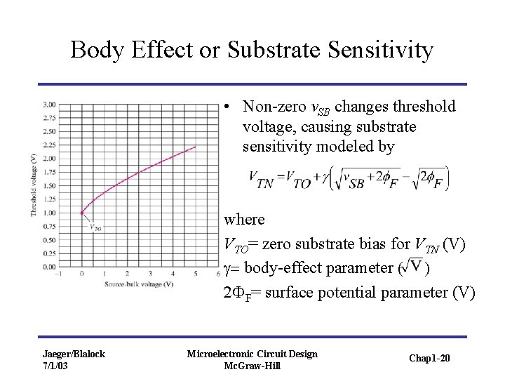
Body Effect or Substrate Sensitivity • Non-zero v. SB changes threshold voltage, causing substrate sensitivity modeled by where VTO= zero substrate bias for VTN (V) g= body-effect parameter ( ) 2 FF= surface potential parameter (V) Jaeger/Blalock 7/1/03 Microelectronic Circuit Design Mc. Graw-Hill Chap 1 -20

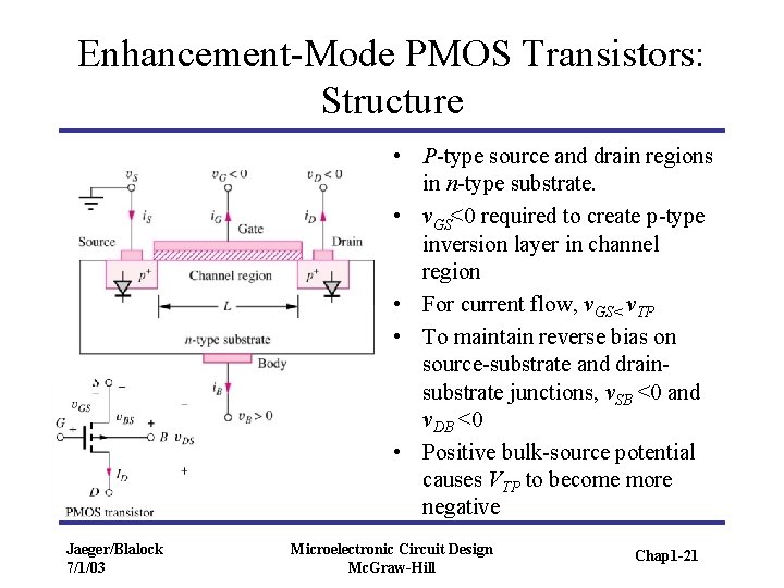
Enhancement-Mode PMOS Transistors: Structure • P-type source and drain regions in n-type substrate. • v. GS<0 required to create p-type inversion layer in channel region • For current flow, v. GS< v. TP • To maintain reverse bias on source-substrate and drainsubstrate junctions, v. SB <0 and v. DB <0 • Positive bulk-source potential causes VTP to become more negative Jaeger/Blalock 7/1/03 Microelectronic Circuit Design Mc. Graw-Hill Chap 1 -21

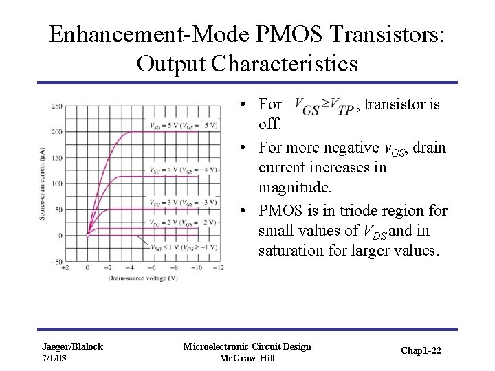
Enhancement-Mode PMOS Transistors: Output Characteristics • For , transistor is off. • For more negative v. GS, drain current increases in magnitude. • PMOS is in triode region for small values of VDS and in saturation for larger values. Jaeger/Blalock 7/1/03 Microelectronic Circuit Design Mc. Graw-Hill Chap 1 -22

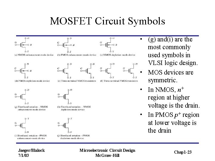
MOSFET Circuit Symbols • (g) and(i) are the most commonly used symbols in VLSI logic design. • MOS devices are symmetric. • In NMOS, n+ region at higher voltage is the drain. • In PMOS p+ region at lower voltage is the drain Jaeger/Blalock 7/1/03 Microelectronic Circuit Design Mc. Graw-Hill Chap 1 -23

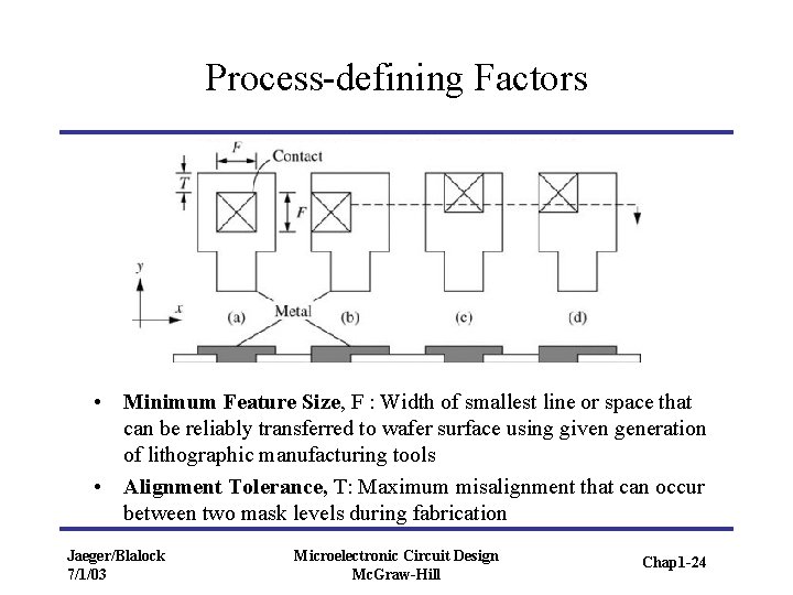
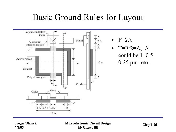
Process-defining Factors • Minimum Feature Size, F : Width of smallest line or space that can be reliably transferred to wafer surface using given generation of lithographic manufacturing tools • Alignment Tolerance, T: Maximum misalignment that can occur between two mask levels during fabrication Jaeger/Blalock 7/1/03 Microelectronic Circuit Design Mc. Graw-Hill Chap 1 -24

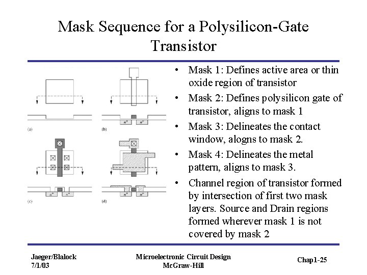
Mask Sequence for a Polysilicon-Gate Transistor • Mask 1: Defines active area or thin oxide region of transistor • Mask 2: Defines polysilicon gate of transistor, aligns to mask 1 • Mask 3: Delineates the contact window, alogns to mask 2. • Mask 4: Delineates the metal pattern, aligns to mask 3. • Channel region of transistor formed by intersection of first two mask layers. Source and Drain regions formed wherever mask 1 is not covered by mask 2 Jaeger/Blalock 7/1/03 Microelectronic Circuit Design Mc. Graw-Hill Chap 1 -25

Basic Ground Rules for Layout • F=2Λ • T=F/2=L, L could be 1, 0. 5, 0. 25 mm, etc. Jaeger/Blalock 7/1/03 Microelectronic Circuit Design Mc. Graw-Hill Chap 1 -26

Internal Capacitances in Electronic Devices • Limit high-frequency performance of the electronic device they are associated with. • Limit switching speed of circuits in logic applications • Limit frequency at which useful amplification can be obtained in amplifiers. • MOSFET capacitances depend on operation region and are non-linear functions of voltages at device terminals. Jaeger/Blalock 7/1/03 Microelectronic Circuit Design Mc. Graw-Hill Chap 1 -27

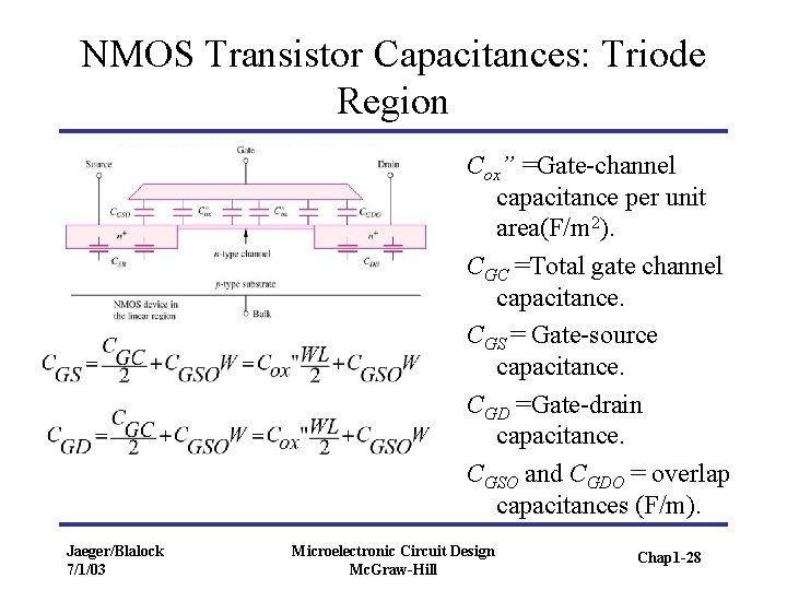
NMOS Transistor Capacitances: Triode Region Cox” =Gate-channel capacitance per unit area(F/m 2). CGC =Total gate channel capacitance. CGS = Gate-source capacitance. CGD =Gate-drain capacitance. CGSO and CGDO = overlap capacitances (F/m). Jaeger/Blalock 7/1/03 Microelectronic Circuit Design Mc. Graw-Hill Chap 1 -28

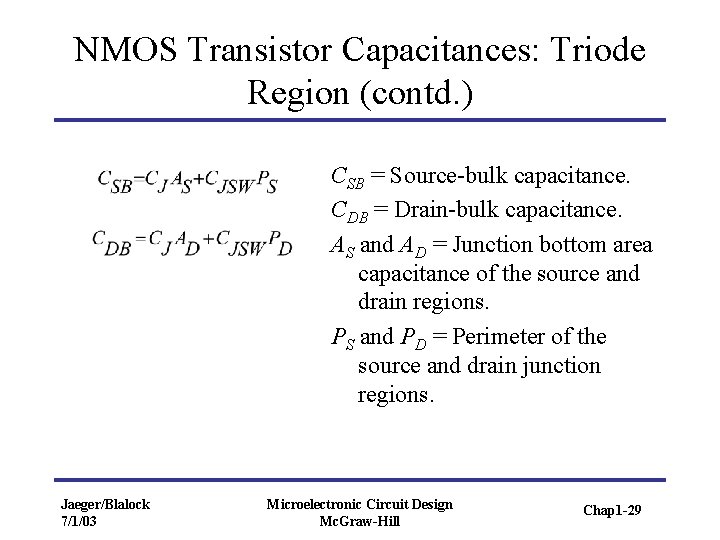
NMOS Transistor Capacitances: Triode Region (contd. ) CSB = Source-bulk capacitance. CDB = Drain-bulk capacitance. AS and AD = Junction bottom area capacitance of the source and drain regions. PS and PD = Perimeter of the source and drain junction regions. Jaeger/Blalock 7/1/03 Microelectronic Circuit Design Mc. Graw-Hill Chap 1 -29

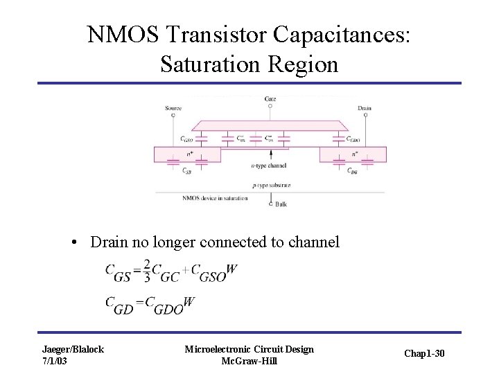
NMOS Transistor Capacitances: Saturation Region • Drain no longer connected to channel Jaeger/Blalock 7/1/03 Microelectronic Circuit Design Mc. Graw-Hill Chap 1 -30

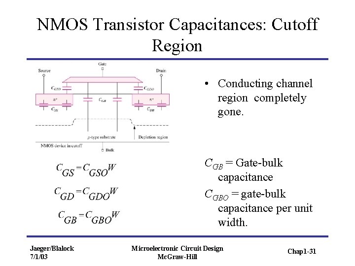
NMOS Transistor Capacitances: Cutoff Region • Conducting channel region completely gone. CGB = Gate-bulk capacitance CGBO = gate-bulk capacitance per unit width. Jaeger/Blalock 7/1/03 Microelectronic Circuit Design Mc. Graw-Hill Chap 1 -31

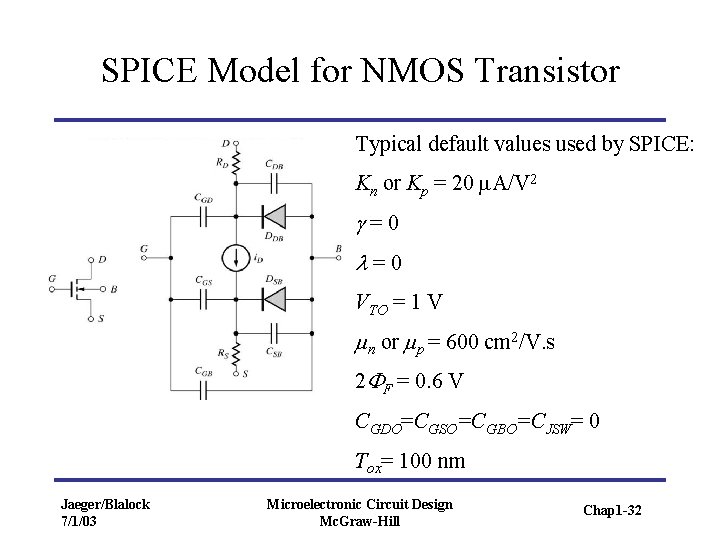
SPICE Model for NMOS Transistor Typical default values used by SPICE: Kn or Kp = 20 m. A/V 2 g=0 l=0 VTO = 1 V mn or mp = 600 cm 2/V. s 2 FF = 0. 6 V CGDO=CGSO=CGBO=CJSW= 0 Tox= 100 nm Jaeger/Blalock 7/1/03 Microelectronic Circuit Design Mc. Graw-Hill Chap 1 -32

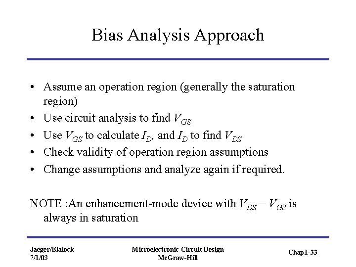
Bias Analysis Approach • Assume an operation region (generally the saturation region) • Use circuit analysis to find VGS • Use VGS to calculate ID, and ID to find VDS • Check validity of operation region assumptions • Change assumptions and analyze again if required. NOTE : An enhancement-mode device with VDS = VGS is always in saturation Jaeger/Blalock 7/1/03 Microelectronic Circuit Design Mc. Graw-Hill Chap 1 -33

Four-Resistor and Two-Resistor Biasing • Provide excellent bias for transistors in discrete circuits. • Stabilize bias point with respect to device parameter and temperature variations using negative feedback. • Use single voltage source to supply both gate-bias voltage and drain current. • Generally used to bias transistors in saturation region. • Two-resistor biasing uses lesser components that fourresistor biasing and also isolates drain and gate terminals Jaeger/Blalock 7/1/03 Microelectronic Circuit Design Mc. Graw-Hill Chap 1 -34

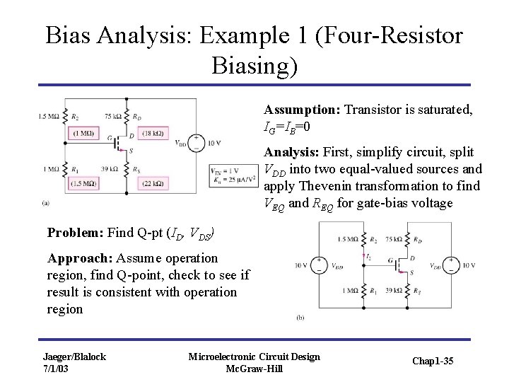
Bias Analysis: Example 1 (Four-Resistor Biasing) Assumption: Transistor is saturated, IG=IB=0 Analysis: First, simplify circuit, split VDD into two equal-valued sources and apply Thevenin transformation to find VEQ and REQ for gate-bias voltage Problem: Find Q-pt (ID, VDS) Approach: Assume operation region, find Q-point, check to see if result is consistent with operation region Jaeger/Blalock 7/1/03 Microelectronic Circuit Design Mc. Graw-Hill Chap 1 -35

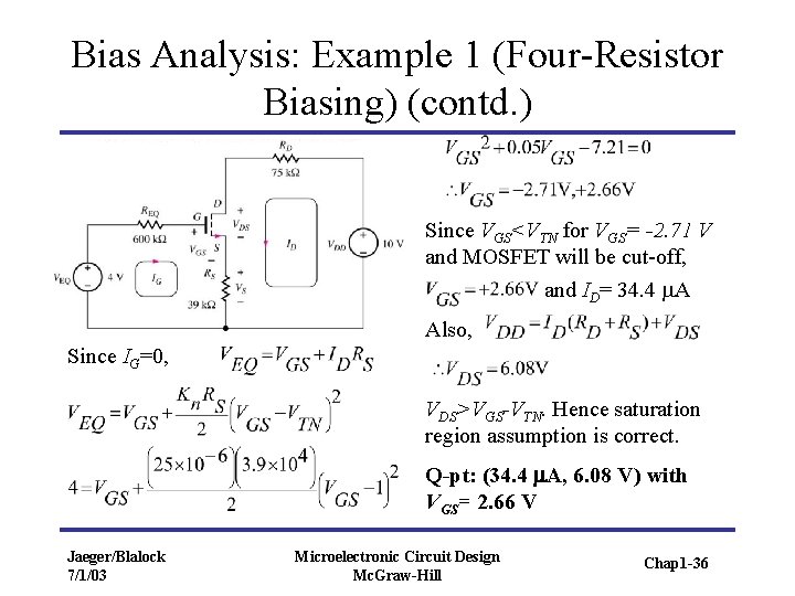
Bias Analysis: Example 1 (Four-Resistor Biasing) (contd. ) Since VGS<VTN for VGS= -2. 71 V and MOSFET will be cut-off, and ID= 34. 4 m. A Also, Since IG=0, VDS>VGS-VTN. Hence saturation region assumption is correct. Q-pt: (34. 4 m. A, 6. 08 V) with VGS= 2. 66 V Jaeger/Blalock 7/1/03 Microelectronic Circuit Design Mc. Graw-Hill Chap 1 -36

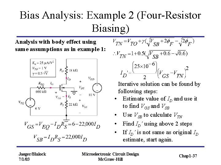
Bias Analysis: Example 2 (Four-Resistor Biasing) Analysis with body effect using same assumptions as in example 1: Iterative solution can be found by following steps: • Estimate value of ID and use it to find VGS and VSB • Use VSB to calculate VTN • Find ID’ using above 2 steps • If ID’ is not same as original ID estimate, start again. Jaeger/Blalock 7/1/03 Microelectronic Circuit Design Mc. Graw-Hill Chap 1 -37

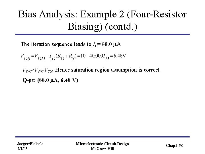
Bias Analysis: Example 2 (Four-Resistor Biasing) (contd. ) The iteration sequence leads to ID= 88. 0 m. A VDS>VGS-VTN. Hence saturation region assumption is correct. Q-pt: (88. 0 m. A, 6. 48 V) Jaeger/Blalock 7/1/03 Microelectronic Circuit Design Mc. Graw-Hill Chap 1 -38

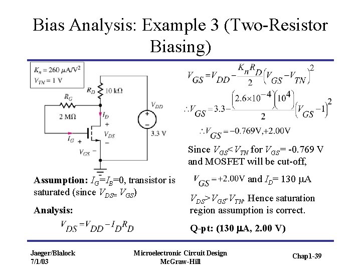
Bias Analysis: Example 3 (Two-Resistor Biasing) Since VGS<VTN for VGS= -0. 769 V and MOSFET will be cut-off, Assumption: IG=IB=0, transistor is saturated (since VDS= VGS) Analysis: and ID= 130 m. A VDS>VGS-VTN. Hence saturation region assumption is correct. Q-pt: (130 m. A, 2. 00 V) Jaeger/Blalock 7/1/03 Microelectronic Circuit Design Mc. Graw-Hill Chap 1 -39

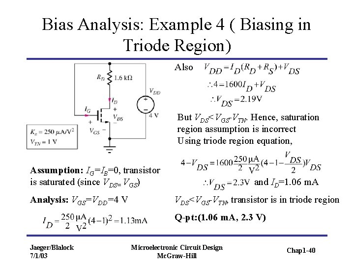
Bias Analysis: Example 4 ( Biasing in Triode Region) Also But VDS<VGS-VTN. Hence, saturation region assumption is incorrect Using triode region equation, Assumption: IG=IB=0, transistor is saturated (since VDS= VGS) Analysis: VGS=VDD=4 V and ID=1. 06 m. A VDS<VGS-VTN, transistor is in triode region Q-pt: (1. 06 m. A, 2. 3 V) Jaeger/Blalock 7/1/03 Microelectronic Circuit Design Mc. Graw-Hill Chap 1 -40

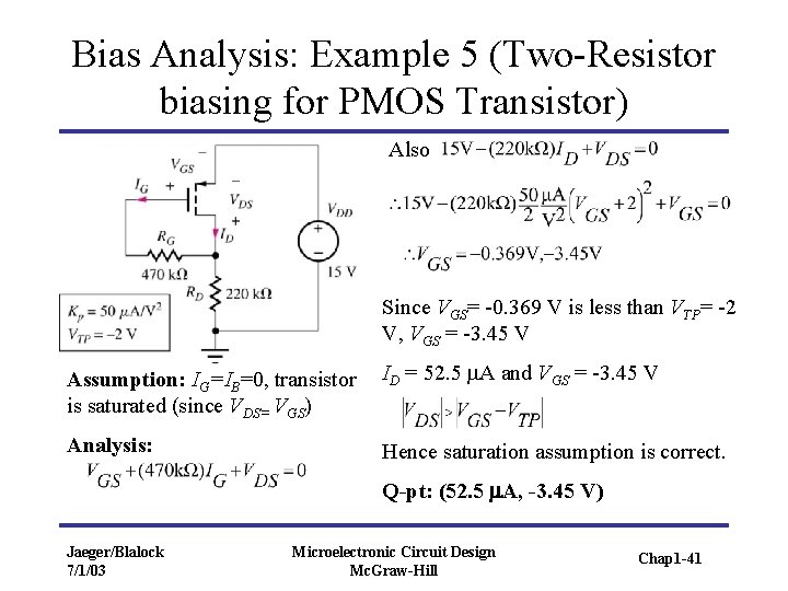
Bias Analysis: Example 5 (Two-Resistor biasing for PMOS Transistor) Also Since VGS= -0. 369 V is less than VTP= -2 V, VGS = -3. 45 V Assumption: IG=IB=0, transistor is saturated (since VDS= VGS) ID = 52. 5 m. A and VGS = -3. 45 V Analysis: Hence saturation assumption is correct. Q-pt: (52. 5 m. A, -3. 45 V) Jaeger/Blalock 7/1/03 Microelectronic Circuit Design Mc. Graw-Hill Chap 1 -41

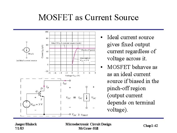
MOSFET as Current Source • Ideal current source gives fixed output current regardless of voltage across it. • MOSFET behaves as as an ideal current source if biased in the pinch-off region (output current depends on terminal voltage). Jaeger/Blalock 7/1/03 Microelectronic Circuit Design Mc. Graw-Hill Chap 1 -42

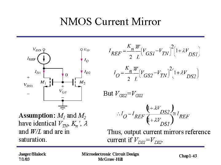
NMOS Current Mirror But VGS 2=VGS 1 Assumption: M 1 and M 2 have identical VTN, Kn’, l and W/L and are in saturation. Jaeger/Blalock 7/1/03 Thus, output current mirrors reference current if VDS 1=VDS 2. Microelectronic Circuit Design Mc. Graw-Hill Chap 1 -43

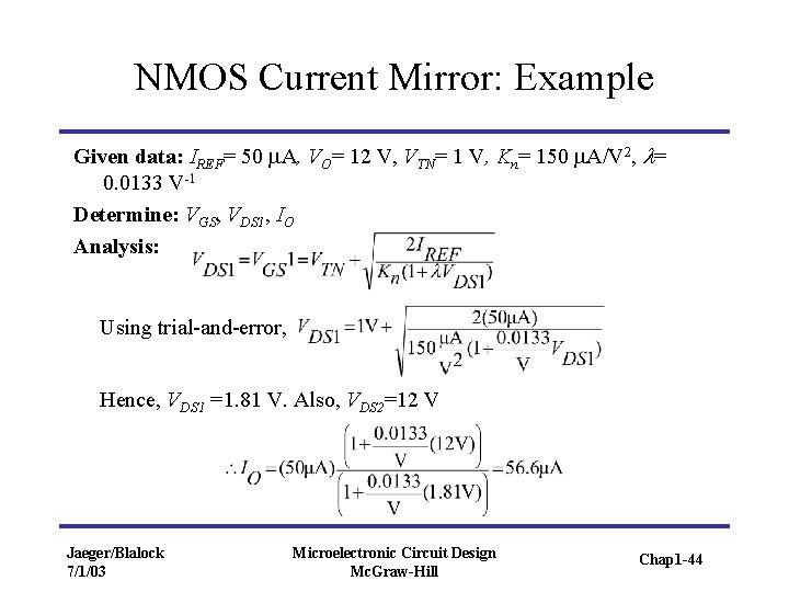
NMOS Current Mirror: Example Given data: IREF= 50 m. A, VO= 12 V, VTN= 1 V, Kn= 150 m. A/V 2, l= 0. 0133 V-1 Determine: VGS, VDS 1, IO Analysis: Using trial-and-error, Hence, VDS 1 =1. 81 V. Also, VDS 2=12 V Jaeger/Blalock 7/1/03 Microelectronic Circuit Design Mc. Graw-Hill Chap 1 -44

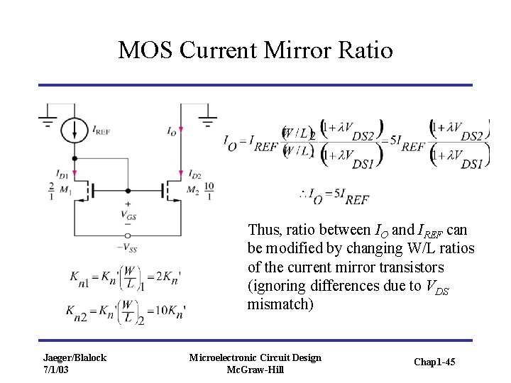
MOS Current Mirror Ratio Thus, ratio between IO and IREF can be modified by changing W/L ratios of the current mirror transistors (ignoring differences due to VDS mismatch) Jaeger/Blalock 7/1/03 Microelectronic Circuit Design Mc. Graw-Hill Chap 1 -45

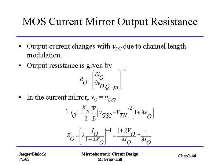
MOS Current Mirror Output Resistance • Output current changes with v. DS due to channel length modulation. • Output resistance is given by • In the current mirror, v. O = v. DS 2 Jaeger/Blalock 7/1/03 Microelectronic Circuit Design Mc. Graw-Hill Chap 1 -46

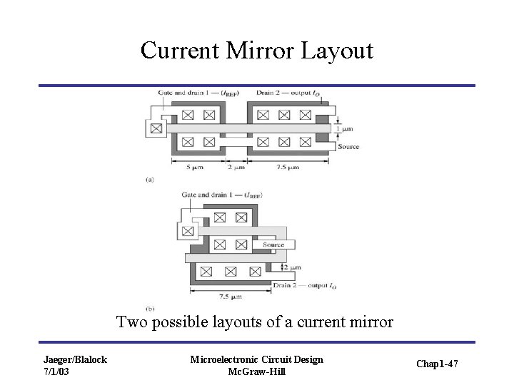
Current Mirror Layout Two possible layouts of a current mirror Jaeger/Blalock 7/1/03 Microelectronic Circuit Design Mc. Graw-Hill Chap 1 -47

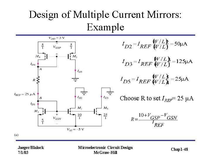
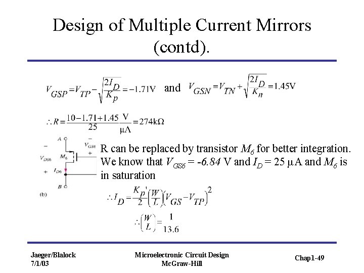
Design of Multiple Current Mirrors: Example Choose R to set IREF= 25 m. A Jaeger/Blalock 7/1/03 Microelectronic Circuit Design Mc. Graw-Hill Chap 1 -48

Design of Multiple Current Mirrors (contd). and R can be replaced by transistor M 6 for better integration. We know that VGS 6 = -6. 84 V and ID = 25 m. A and M 6 is in saturation Jaeger/Blalock 7/1/03 Microelectronic Circuit Design Mc. Graw-Hill Chap 1 -49

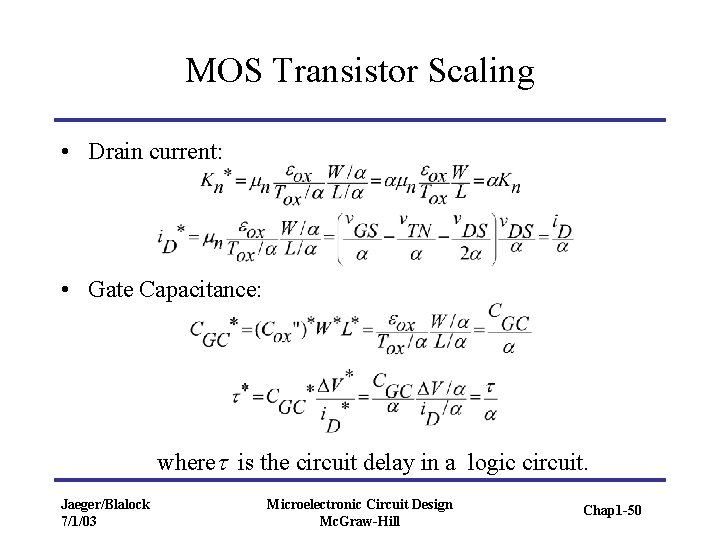
MOS Transistor Scaling • Drain current: • Gate Capacitance: wheret is the circuit delay in a logic circuit. Jaeger/Blalock 7/1/03 Microelectronic Circuit Design Mc. Graw-Hill Chap 1 -50

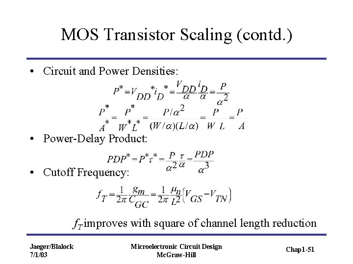
MOS Transistor Scaling (contd. ) • Circuit and Power Densities: • Power-Delay Product: • Cutoff Frequency: f. T improves with square of channel length reduction Jaeger/Blalock 7/1/03 Microelectronic Circuit Design Mc. Graw-Hill Chap 1 -51

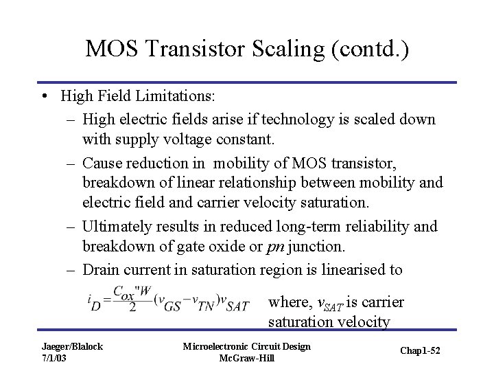
MOS Transistor Scaling (contd. ) • High Field Limitations: – High electric fields arise if technology is scaled down with supply voltage constant. – Cause reduction in mobility of MOS transistor, breakdown of linear relationship between mobility and electric field and carrier velocity saturation. – Ultimately results in reduced long-term reliability and breakdown of gate oxide or pn junction. – Drain current in saturation region is linearised to where, v. SAT is carrier saturation velocity Jaeger/Blalock 7/1/03 Microelectronic Circuit Design Mc. Graw-Hill Chap 1 -52

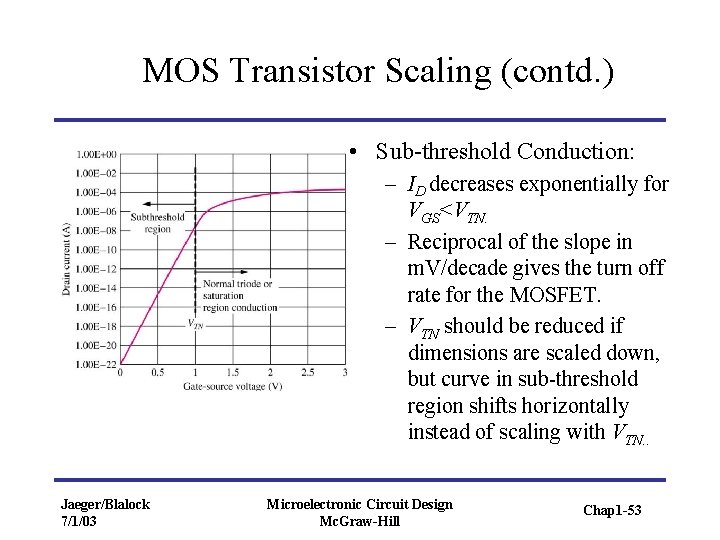
MOS Transistor Scaling (contd. ) • Sub-threshold Conduction: – ID decreases exponentially for VGS<VTN. – Reciprocal of the slope in m. V/decade gives the turn off rate for the MOSFET. – VTN should be reduced if dimensions are scaled down, but curve in sub-threshold region shifts horizontally instead of scaling with VTN. . Jaeger/Blalock 7/1/03 Microelectronic Circuit Design Mc. Graw-Hill Chap 1 -53

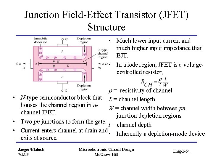
Junction Field-Effect Transistor (JFET) Structure • Much lower input current and much higher input impedance than BJT. • In triode region, JFET is a voltagecontrolled resistor, r = resistivity of channel • N-type semiconductor block that L = channel length houses the channel region in n. W = channel width between pn channel JFET. junction depletion regions • Two pn junctions to form the gate. t = channel depth • Current enters channel at drain and • Inherently a depletion-mode device exits at source. Jaeger/Blalock 7/1/03 Microelectronic Circuit Design Mc. Graw-Hill Chap 1 -54

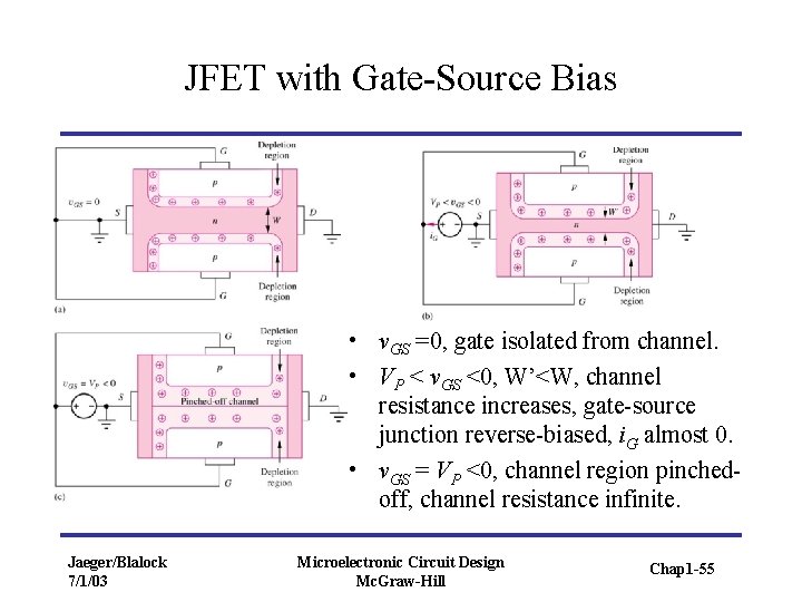
JFET with Gate-Source Bias • v. GS =0, gate isolated from channel. • VP < v. GS <0, W’<W, channel resistance increases, gate-source junction reverse-biased, i. G almost 0. • v. GS = VP <0, channel region pinchedoff, channel resistance infinite. Jaeger/Blalock 7/1/03 Microelectronic Circuit Design Mc. Graw-Hill Chap 1 -55

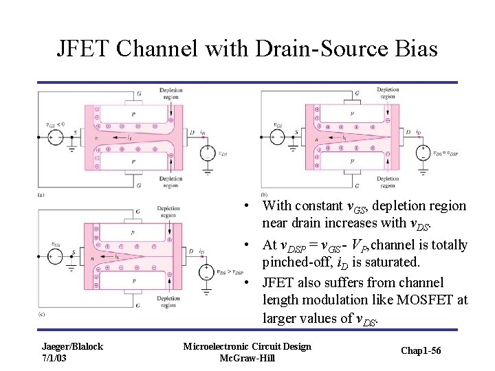
JFET Channel with Drain-Source Bias • With constant v. GS, depletion region near drain increases with v. DS. • At v. DSP = v. GS - VP, channel is totally pinched-off, i. D is saturated. • JFET also suffers from channel length modulation like MOSFET at larger values of v. DS. Jaeger/Blalock 7/1/03 Microelectronic Circuit Design Mc. Graw-Hill Chap 1 -56

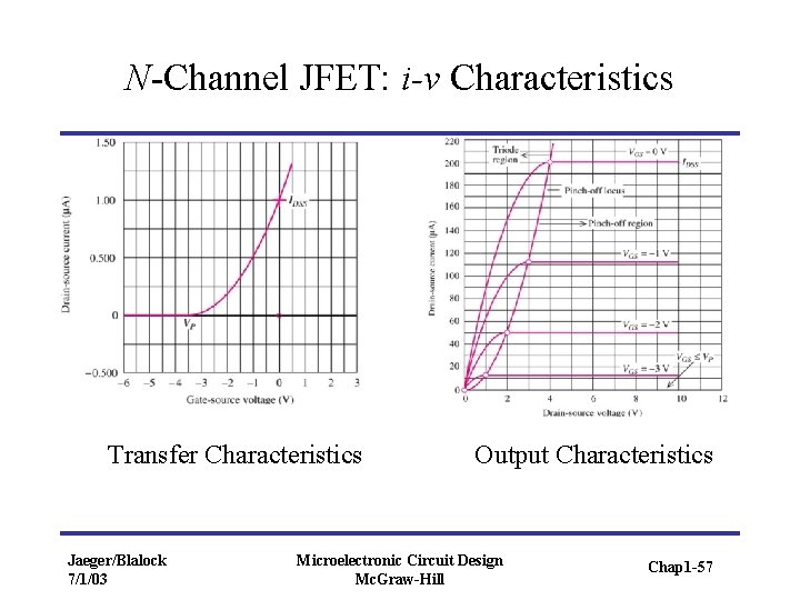
N-Channel JFET: i-v Characteristics Transfer Characteristics Jaeger/Blalock 7/1/03 Output Characteristics Microelectronic Circuit Design Mc. Graw-Hill Chap 1 -57

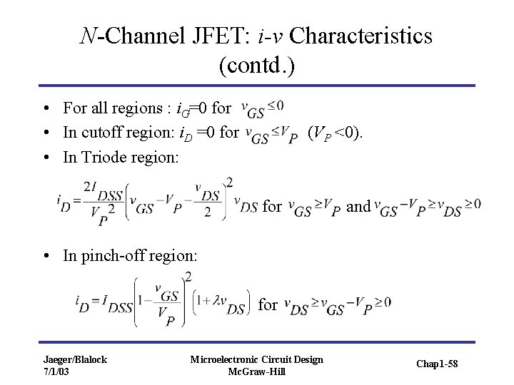
N-Channel JFET: i-v Characteristics (contd. ) • For all regions : i. G=0 for • In cutoff region: i. D =0 for • In Triode region: (VP <0). for and • In pinch-off region: for Jaeger/Blalock 7/1/03 Microelectronic Circuit Design Mc. Graw-Hill Chap 1 -58

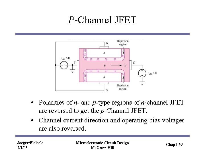
P-Channel JFET • Polarities of n- and p-type regions of n-channel JFET are reversed to get the p-Channel JFET. • Channel current direction and operating bias voltages are also reversed. Jaeger/Blalock 7/1/03 Microelectronic Circuit Design Mc. Graw-Hill Chap 1 -59

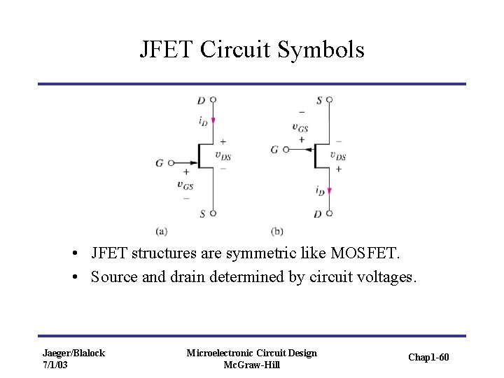
JFET Circuit Symbols • JFET structures are symmetric like MOSFET. • Source and drain determined by circuit voltages. Jaeger/Blalock 7/1/03 Microelectronic Circuit Design Mc. Graw-Hill Chap 1 -60

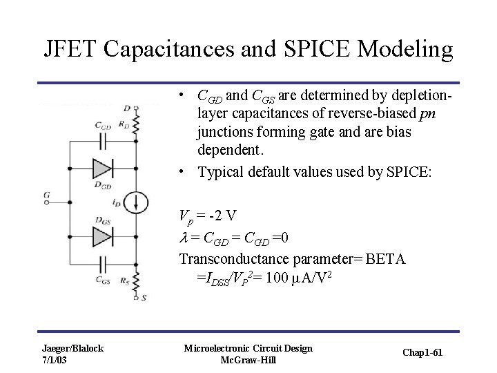
JFET Capacitances and SPICE Modeling • CGD and CGS are determined by depletionlayer capacitances of reverse-biased pn junctions forming gate and are bias dependent. • Typical default values used by SPICE: Vp = -2 V l = CGD =0 Transconductance parameter= BETA =IDSS/VP 2= 100 m. A/V 2 Jaeger/Blalock 7/1/03 Microelectronic Circuit Design Mc. Graw-Hill Chap 1 -61

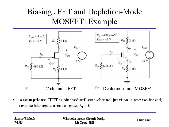
Biasing JFET and Depletion-Mode MOSFET: Example N-channel JFET Depletion-mode MOSFET • Assumptions: JFET is pinched-off, gate-channel junction is reverse-biased, reverse leakage current of gate, IG = 0 Jaeger/Blalock 7/1/03 Microelectronic Circuit Design Mc. Graw-Hill Chap 1 -62

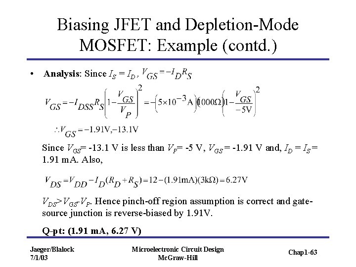
Biasing JFET and Depletion-Mode MOSFET: Example (contd. ) • Analysis: Since IS = ID , Since VGS= -13. 1 V is less than VP= -5 V, VGS = -1. 91 V and, ID = IS = 1. 91 m. A. Also, VDS>VGS-VP. Hence pinch-off region assumption is correct and gatesource junction is reverse-biased by 1. 91 V. Q-pt: (1. 91 m. A, 6. 27 V) Jaeger/Blalock 7/1/03 Microelectronic Circuit Design Mc. Graw-Hill Chap 1 -63