Chapter 4 Field effect transistor Introduction Organic FETs

- Slides: 42

Chapter 4. Field effect transistor

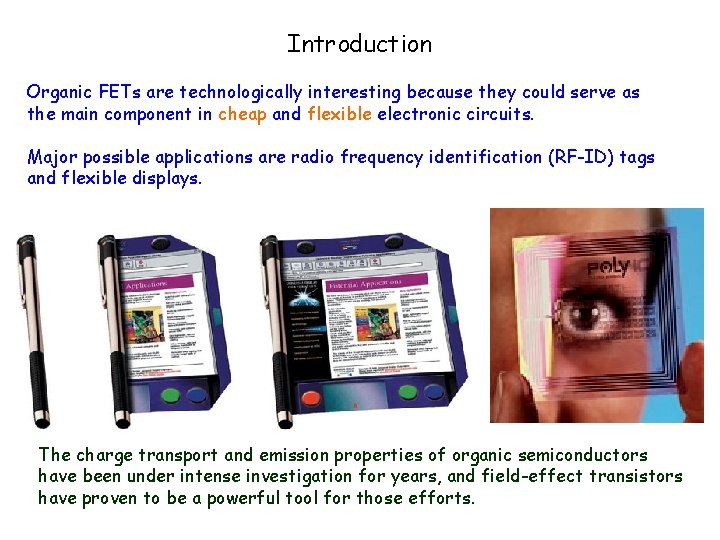
Introduction Organic FETs are technologically interesting because they could serve as the main component in cheap and flexible electronic circuits. Major possible applications are radio frequency identification (RF-ID) tags and flexible displays. The charge transport and emission properties of organic semiconductors have been under intense investigation for years, and field-effect transistors have proven to be a powerful tool for those efforts.

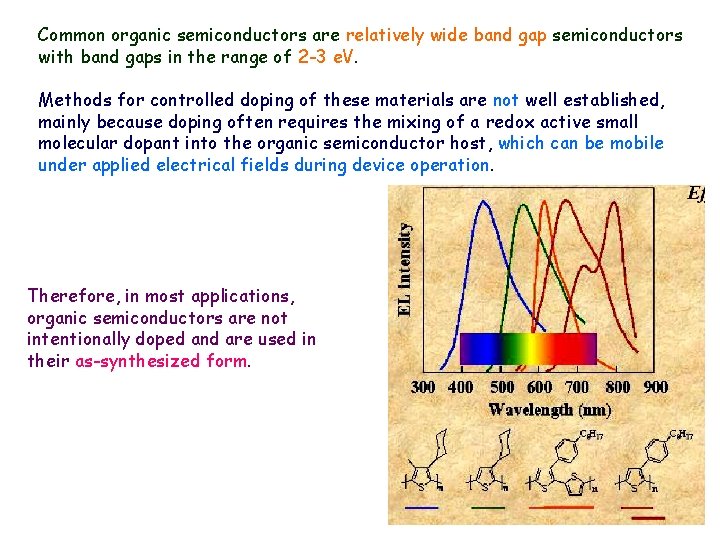
Common organic semiconductors are relatively wide band gap semiconductors with band gaps in the range of 2 -3 e. V. Methods for controlled doping of these materials are not well established, mainly because doping often requires the mixing of a redox active small molecular dopant into the organic semiconductor host, which can be mobile under applied electrical fields during device operation. Therefore, in most applications, organic semiconductors are not intentionally doped and are used in their as-synthesized form.


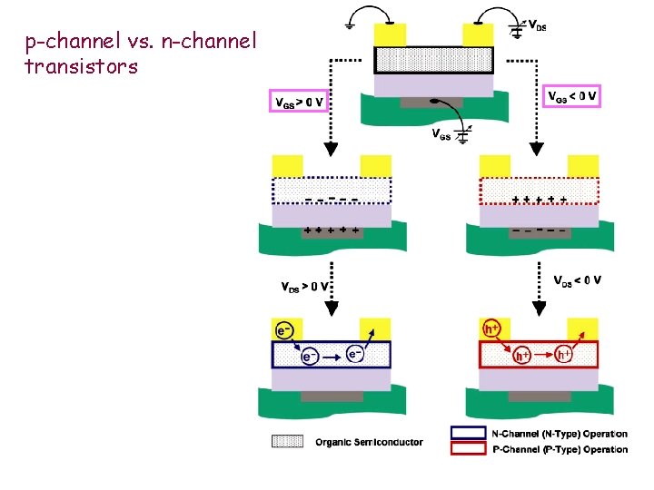
For many organic semiconductor-based FETs, only p-channel operation seems possible. For this reason, such materials have been called “p-type” organic semiconductors. Over the last 5 years, many groups have aimed to realize “n-type” organic FETs. This usually involved the synthesis of special organic semi-conductors with high electron affinities, comprising specific electron withdrawing groups. These were then called “n-type” organic semiconductors Processing and characterization conditions, device architecture, and choice of electrodes are important as well. It is thus not appropriate to speak of ptype or n-type materials, but one should rather refer to p-channel or n-channel transistors.

p-channel vs. n-channel transistors

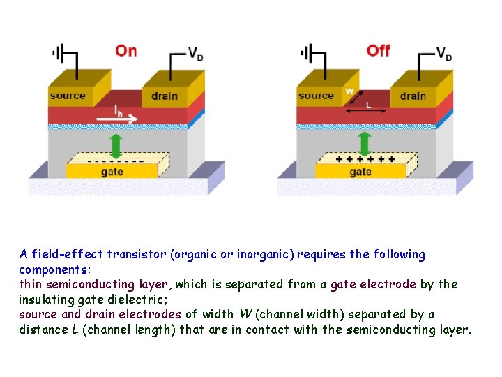
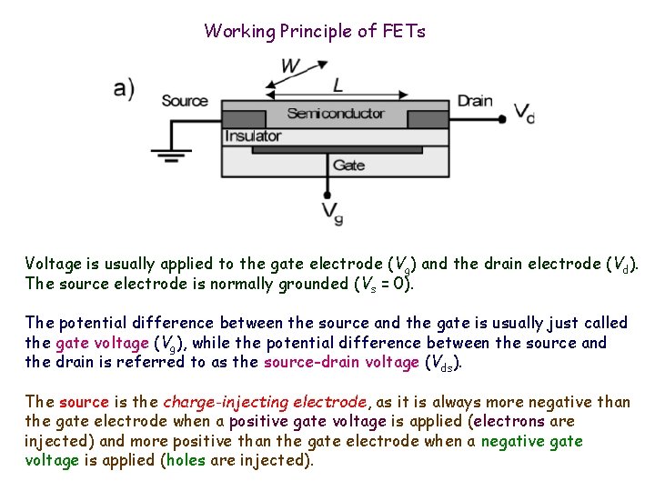
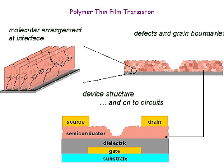
A field-effect transistor (organic or inorganic) requires the following components: thin semiconducting layer, which is separated from a gate electrode by the insulating gate dielectric; source and drain electrodes of width W (channel width) separated by a distance L (channel length) that are in contact with the semiconducting layer.


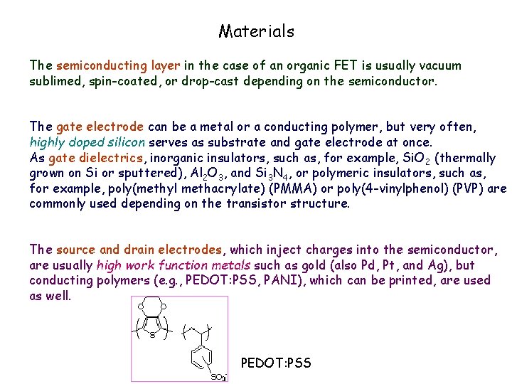
Materials The semiconducting layer in the case of an organic FET is usually vacuum sublimed, spin-coated, or drop-cast depending on the semiconductor. The gate electrode can be a metal or a conducting polymer, but very often, highly doped silicon serves as substrate and gate electrode at once. As gate dielectrics, inorganic insulators, such as, for example, Si. O 2 (thermally grown on Si or sputtered), Al 2 O 3, and Si 3 N 4, or polymeric insulators, such as, for example, poly(methyl methacrylate) (PMMA) or poly(4 -vinylphenol) (PVP) are commonly used depending on the transistor structure. The source and drain electrodes, which inject charges into the semiconductor, are usually high work function metals such as gold (also Pd, Pt, and Ag), but conducting polymers (e. g. , PEDOT: PSS, PANI), which can be printed, are used as well. PEDOT: PSS

Working Principle of FETs Voltage is usually applied to the gate electrode (Vg) and the drain electrode (Vd). The source electrode is normally grounded (Vs = 0). The potential difference between the source and the gate is usually just called the gate voltage (Vg), while the potential difference between the source and the drain is referred to as the source-drain voltage (Vds). The source is the charge-injecting electrode, as it is always more negative than the gate electrode when a positive gate voltage is applied (electrons are injected) and more positive than the gate electrode when a negative gate voltage is applied (holes are injected).

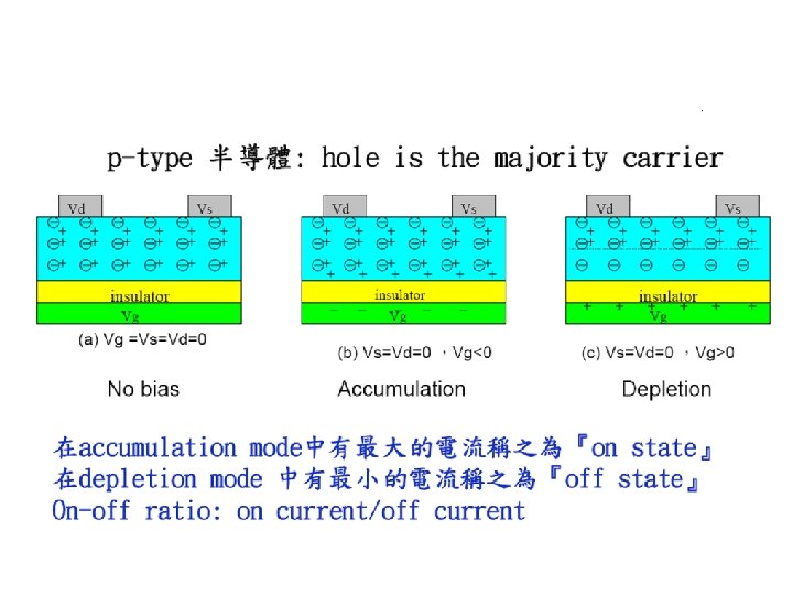
Assume a simple metal-insulator semiconductor (MIS) diode (that is, there is no potential difference between source and drain) with a voltage Vg applied to the gate electrode. A positive gate voltage for example will induce negative charges (electrons) at the insulator/semiconductor interface that were injected from the grounded electrodes. For negative Vg, positive charges (holes) will be accumulated. The number of accumulated charges is proportional to Vg and the capacitance Ci of the insulator. However, not all induced charges are mobile and will thus contribute to the current in a field-effect transistor. Deep traps first have to be filled before the additionally induced charges can be mobile. That is, a gate voltage has to be applied that is higher than a threshold voltage VTh, and thus, the effective gate voltage is Vg - VTh. On the other hand, donor (for n-channel) or acceptor (for p-channel) states and interface dipoles can create an internal potential at the interface and thus cause accumulation of charges in the channel when Vg = 0 so that in some cases an opposite voltage has to be applied to turn the channel off.

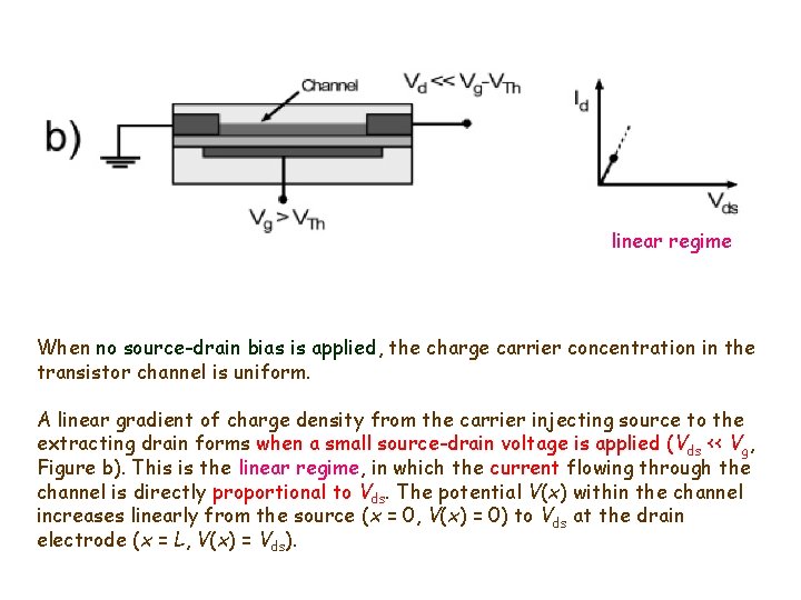
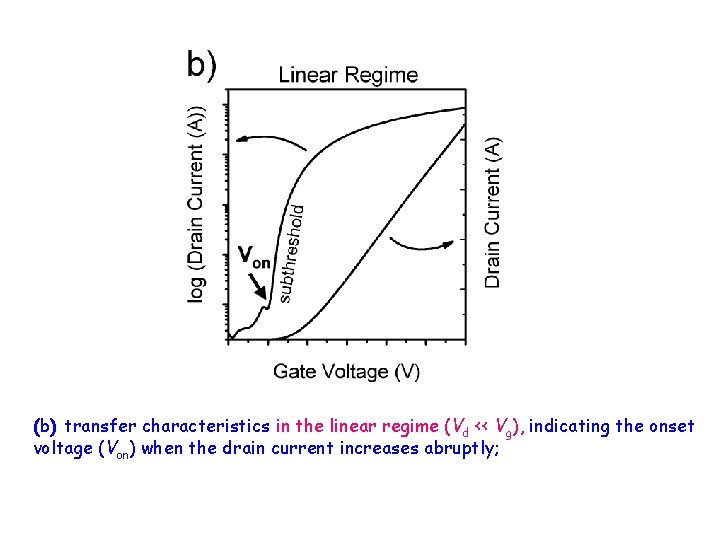
linear regime When no source-drain bias is applied, the charge carrier concentration in the transistor channel is uniform. A linear gradient of charge density from the carrier injecting source to the extracting drain forms when a small source-drain voltage is applied (Vds << Vg, Figure b). This is the linear regime, in which the current flowing through the channel is directly proportional to Vds. The potential V(x) within the channel increases linearly from the source (x = 0, V(x) = 0) to Vds at the drain electrode (x = L, V(x) = Vds).

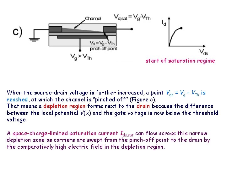
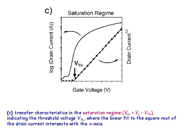
start of saturation regime When the source-drain voltage is further increased, a point Vds = Vg - VTh is reached, at which the channel is “pinched off” (Figure c). That means a depletion region forms next to the drain because the difference between the local potential V(x) and the gate voltage is now below the threshold voltage. A space-charge-limited saturation current Ids, sat can flow across this narrow depletion zone as carriers are swept from the pinch-off point to the drain by the comparatively high electric field in the depletion region.

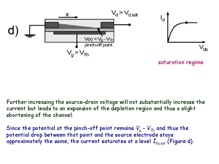
saturation regime Further increasing the source-drain voltage will not substantially increase the current but leads to an expansion of the depletion region and thus a slight shortening of the channel. Since the potential at the pinch-off point remains Vg - VTh and thus the potential drop between that point and the source electrode stays approximately the same, the current saturates at a level Ids, sat (Figure d).

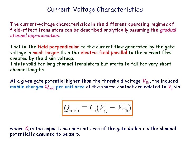
Current-Voltage Characteristics The current-voltage characteristics in the different operating regimes of field-effect transistors can be described analytically assuming the gradual channel approximation. That is, the field perpendicular to the current flow generated by the gate voltage is much larger than the electric field parallel to the current flow created by the drain voltage. This is valid for long channel transistors but starts to fail for very short channel lengths At a given gate potential higher than the threshold voltage VTh, the induced mobile charges Qmob per unit area at the source contact are related to Vg via where Ci is the capacitance per unit area of the gate dielectric the channel potential is assumed to be zero.

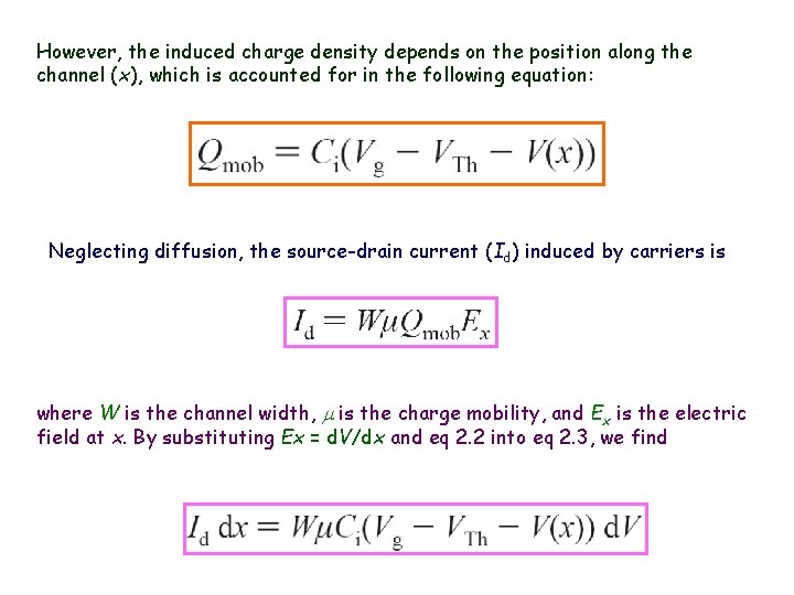
However, the induced charge density depends on the position along the channel (x), which is accounted for in the following equation: Neglecting diffusion, the source-drain current (Id) induced by carriers is where W is the channel width, m is the charge mobility, and Ex is the electric field at x. By substituting Ex = d. V/dx and eq 2. 2 into eq 2. 3, we find

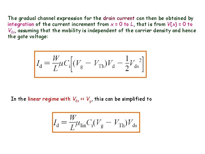
The gradual channel expression for the drain current can then be obtained by integration of the current increment from x = 0 to L, that is from V(x) = 0 to Vds, assuming that the mobility is independent of the carrier density and hence the gate voltage: In the linear regime with Vds << Vg, this can be simplified to

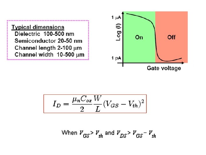
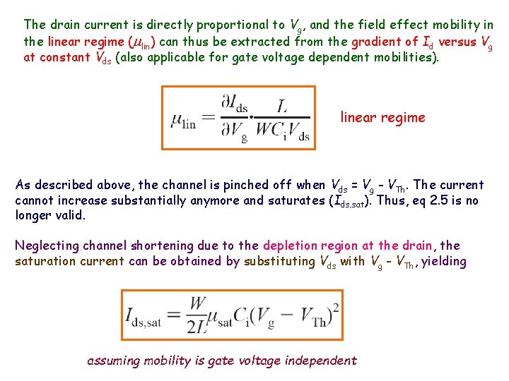
The drain current is directly proportional to Vg, and the field effect mobility in the linear regime (mlin) can thus be extracted from the gradient of Id versus Vg at constant Vds (also applicable for gate voltage dependent mobilities). linear regime As described above, the channel is pinched off when Vds = Vg - VTh. The current cannot increase substantially anymore and saturates (Ids, sat). Thus, eq 2. 5 is no longer valid. Neglecting channel shortening due to the depletion region at the drain, the saturation current can be obtained by substituting Vds with Vg - VTh, yielding assuming mobility is gate voltage independent

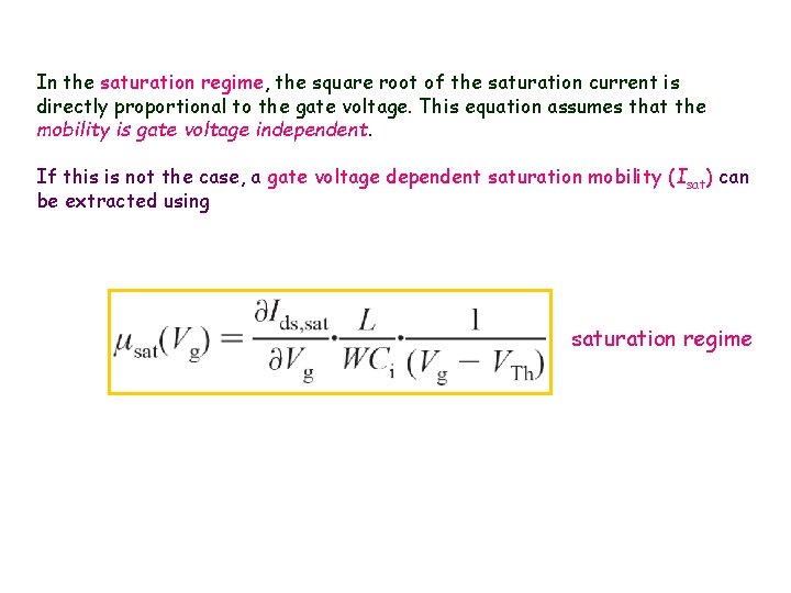
In the saturation regime, the square root of the saturation current is directly proportional to the gate voltage. This equation assumes that the mobility is gate voltage independent. If this is not the case, a gate voltage dependent saturation mobility (Isat) can be extracted using saturation regime

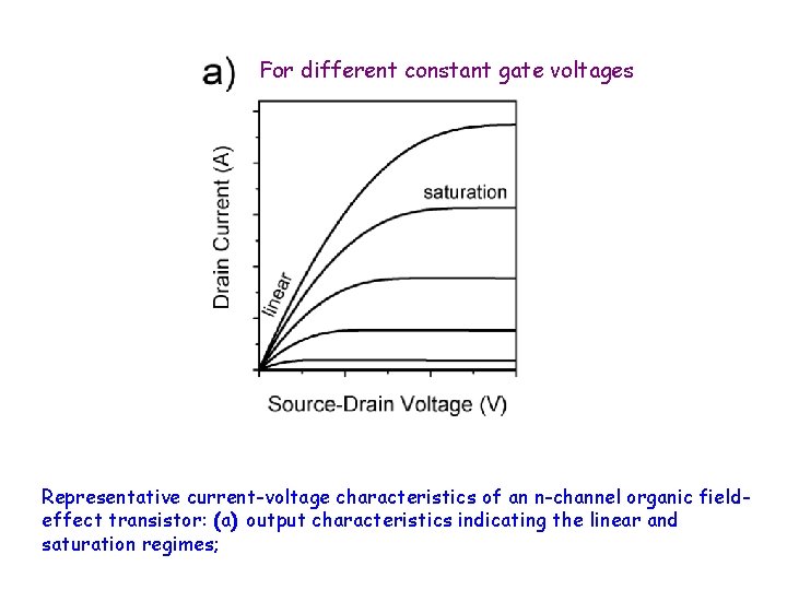
For different constant gate voltages Representative current-voltage characteristics of an n-channel organic fieldeffect transistor: (a) output characteristics indicating the linear and saturation regimes;

(b) transfer characteristics in the linear regime (Vd << Vg), indicating the onset voltage (Von) when the drain current increases abruptly;

(c) transfer characteristics in the saturation regime (Vds > Vg - VTh), indicating the threshold voltage VTh, where the linear fit to the square root of the drain current intersects with the x-axis.


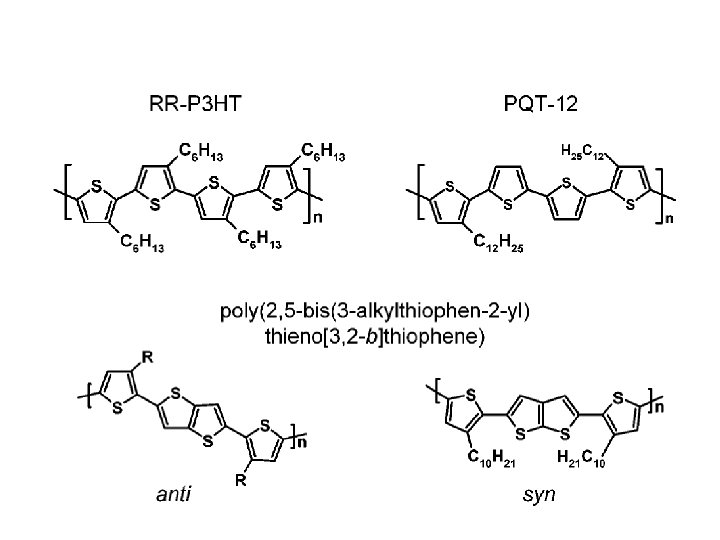
Polymer Thin Film Transistor

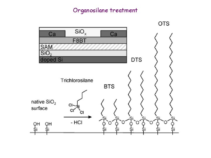
Organosilane treatment

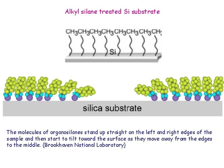
Alkyl silane treated Si substrate The molecules of organosilanes stand up straight on the left and right edges of the sample and then start to tilt toward the surface as they move away from the edges to the middle. (Brookhaven National Laboratory)

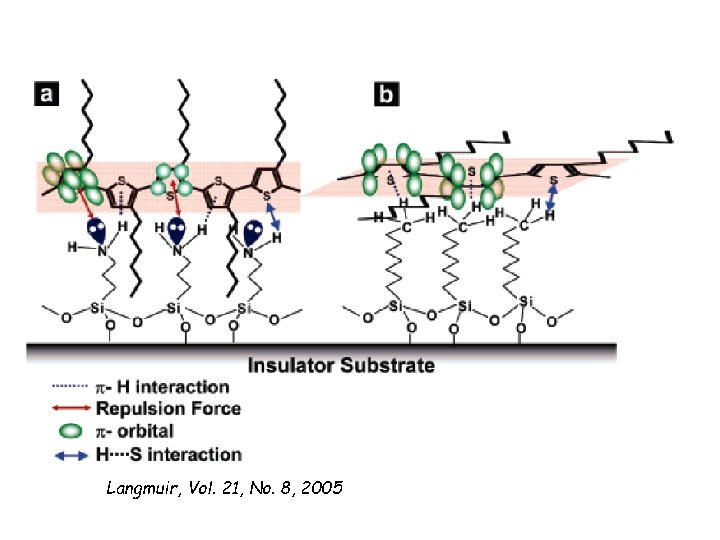
Langmuir, Vol. 21, No. 8, 2005

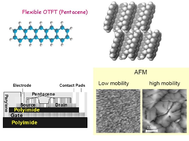
Flexible OTFT (Pentacene)

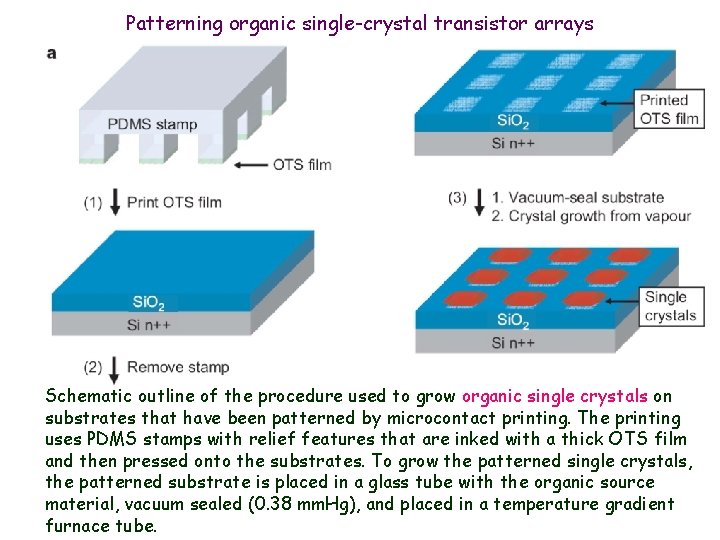
Patterning organic single-crystal transistor arrays Schematic outline of the procedure used to grow organic single crystals on substrates that have been patterned by microcontact printing. The printing uses PDMS stamps with relief features that are inked with a thick OTS film and then pressed onto the substrates. To grow the patterned single crystals, the patterned substrate is placed in a glass tube with the organic source material, vacuum sealed (0. 38 mm. Hg), and placed in a temperature gradient furnace tube.

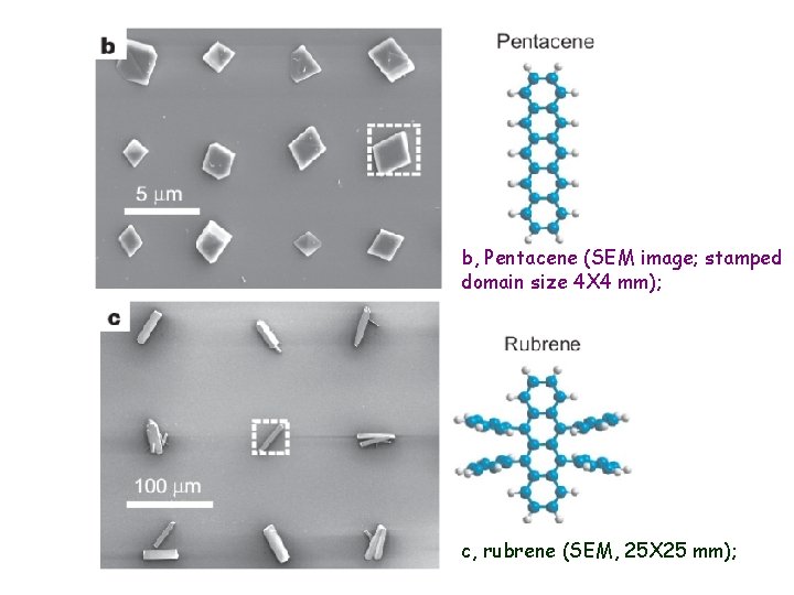
b, Pentacene (SEM image; stamped domain size 4 X 4 mm); c, rubrene (SEM, 25 X 25 mm);

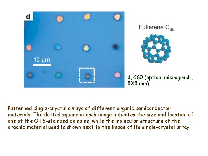
d, C 60 (optical micrograph, 8 X 8 mm) Patterned single-crystal arrays of different organic semiconductor materials. The dotted square in each image indicates the size and location of one of the OTS-stamped domains, while the molecular structure of the organic material used is shown next to the image of its single-crystal array.

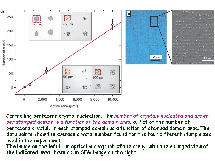
Controlling pentacene crystal nucleation. The number of crystals nucleated and grown per stamped domain is a function of the domain area. a, Plot of the number of pentacene crystals in each stamped domain as a function of stamped domain area. The data points show the average crystal number found for the four different stamp sizes used in the experiment. The image on the left is an optical micrograph of the array, with the enlarged view of the indicated area shown as an SEM image on the right.

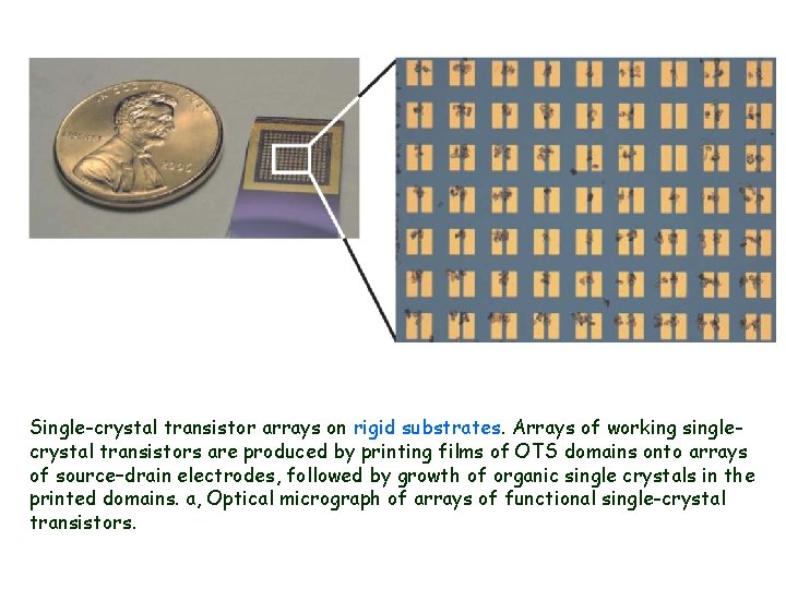
Single-crystal transistor arrays on rigid substrates. Arrays of working singlecrystal transistors are produced by printing films of OTS domains onto arrays of source–drain electrodes, followed by growth of organic single crystals in the printed domains. a, Optical micrograph of arrays of functional single-crystal transistors.

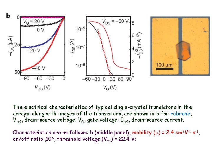
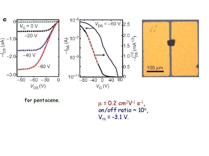
The electrical characteristics of typical single-crystal transistors in the arrays, along with images of the transistors, are shown in b for rubrene, VDS, drain–source voltage; VG, gate voltage; IDS, drain–source current. Characteristics are as follows: b (middle panel), mobility (m) = 2. 4 cm 2 V-1 s-1, on/off ratio , 106, threshold voltage (Vth) = 22. 4 V;

for pentacene. m = 0. 2 cm 2 V-1 s-1, on/off ratio ~ 106, Vth = -3. 1 V.

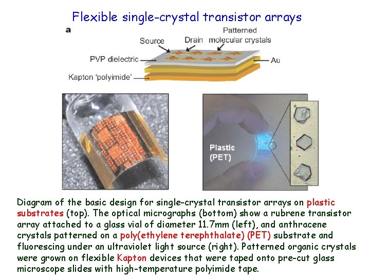
Flexible single-crystal transistor arrays Diagram of the basic design for single-crystal transistor arrays on plastic substrates (top). The optical micrographs (bottom) show a rubrene transistor array attached to a glass vial of diameter 11. 7 mm (left), and anthracene crystals patterned on a poly(ethylene terephthalate) (PET) substrate and fluorescing under an ultraviolet light source (right). Patterned organic crystals were grown on flexible Kapton devices that were taped onto pre-cut glass microscope slides with high-temperature polyimide tape.

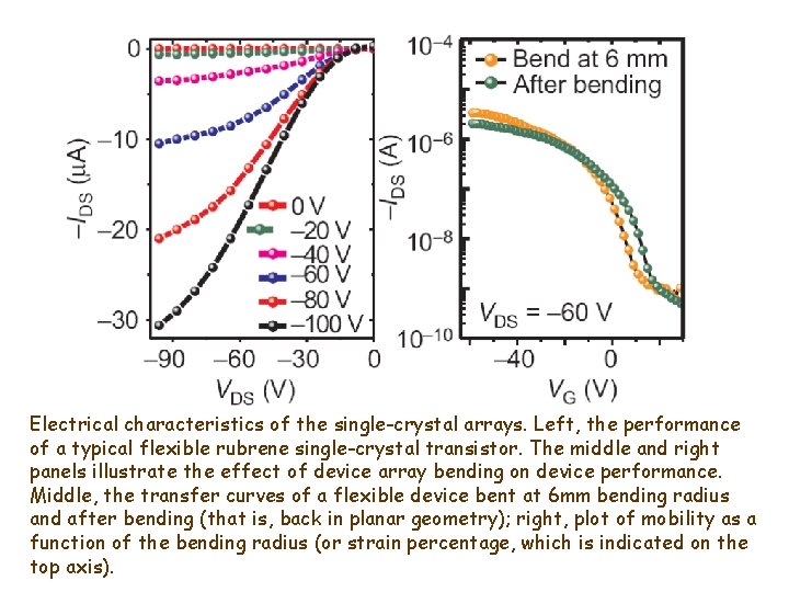
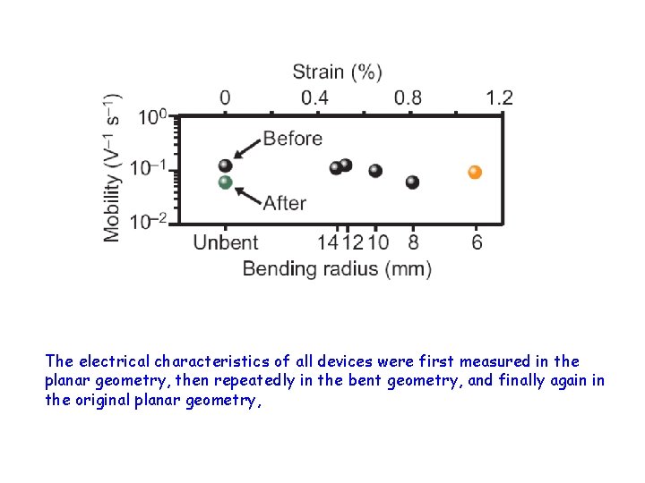
Electrical characteristics of the single-crystal arrays. Left, the performance of a typical flexible rubrene single-crystal transistor. The middle and right panels illustrate the effect of device array bending on device performance. Middle, the transfer curves of a flexible device bent at 6 mm bending radius and after bending (that is, back in planar geometry); right, plot of mobility as a function of the bending radius (or strain percentage, which is indicated on the top axis).

The electrical characteristics of all devices were first measured in the planar geometry, then repeatedly in the bent geometry, and finally again in the original planar geometry,

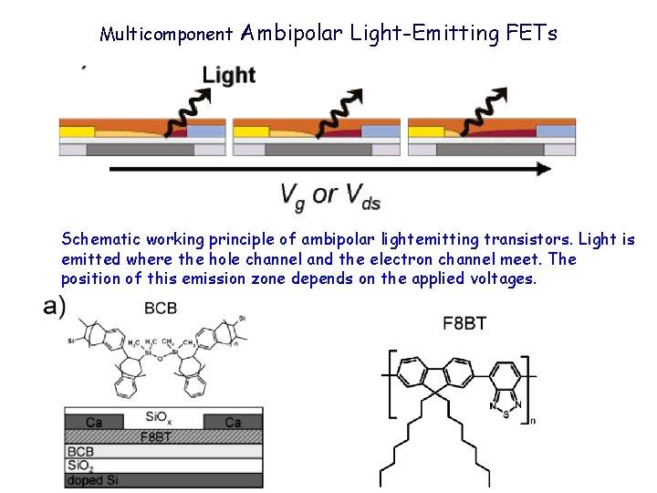
Multicomponent Ambipolar Light-Emitting FETs Schematic working principle of ambipolar lightemitting transistors. Light is emitted where the hole channel and the electron channel meet. The position of this emission zone depends on the applied voltages.

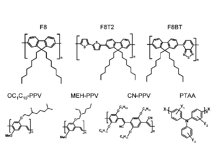
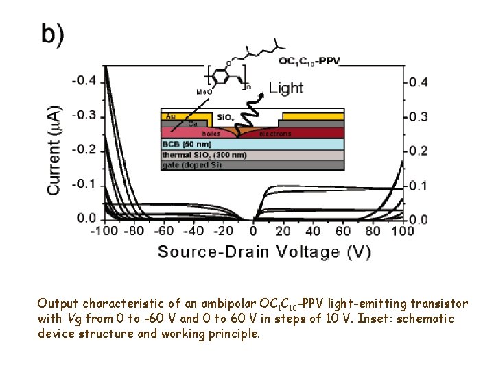
Output characteristic of an ambipolar OC 1 C 10 -PPV light-emitting transistor with Vg from 0 to -60 V and 0 to 60 V in steps of 10 V. Inset: schematic device structure and working principle.

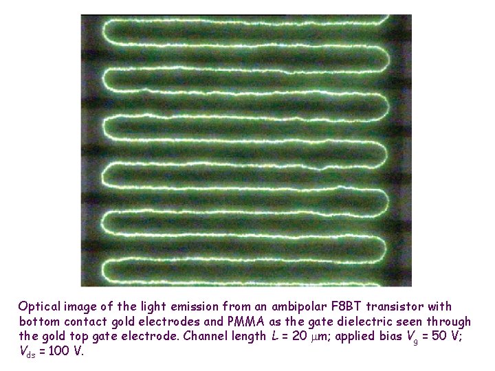
Optical image of the light emission from an ambipolar F 8 BT transistor with bottom contact gold electrodes and PMMA as the gate dielectric seen through the gold top gate electrode. Channel length L = 20 mm; applied bias Vg = 50 V; Vds = 100 V.