Chapter 4 DC BiasingBJTs Introduction the transistor is
Chapter 4 DC Biasing–BJTs
Introduction • the transistor is a magical device that can raise the level of the applied ac input without the assistance of an external energy source. • In actuality, the improved output ac power level is the result of a transfer of energy from the applied dc supplies. • The analysis or design of any electronic amplifier therefore has two components: the dc portion and the ac portion. Electronic Devices and Circuit Theory, 10/e Robert L. Boylestad and Louis Nashelsky Copyright © 2009 by Pearson Education, Inc. Upper Saddle River, New Jersey 07458 • All rights reserved.
Biasing: The DC voltages applied to a transistor in order to turn it on so that it can amplify the AC signal. The term biasing is an all-inclusive term for the application of dc voltages to establish a fixed level of current and voltage. DC Biasing – used to set the initial values of IB, IC, and VCE for ac operation of the transistor For transistor amplifiers the resulting dc current and voltage establish an operating point, Since the operating point is a fixed point on the characteristics, it is also called the quiescent point (abbreviated Q-point). Electronic Devices and Circuit Theory, 10/e Robert L. Boylestad and Louis Nashelsky Copyright © 2009 by Pearson Education, Inc. Upper Saddle River, New Jersey 07458 • All rights reserved.
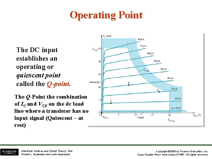
Operating Point The DC input establishes an operating or quiescent point called the Q-point The Q-Point the combination of IC and VCE on the dc load line where a transistor has no input signal (Quiescent – at rest) Electronic Devices and Circuit Theory, 10/e Robert L. Boylestad and Louis Nashelsky Copyright © 2009 by Pearson Education, Inc. Upper Saddle River, New Jersey 07458 • All rights reserved.
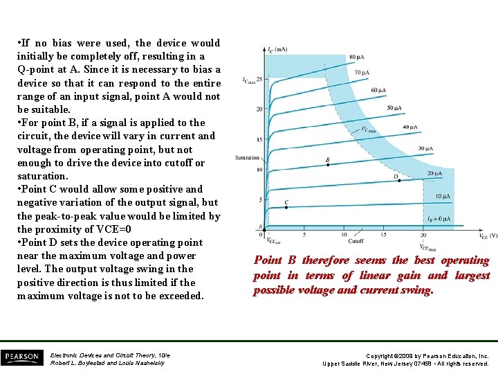
• If no bias were used, the device would initially be completely off, resulting in a Q-point at A. Since it is necessary to bias a device so that it can respond to the entire range of an input signal, point A would not be suitable. • For point B, if a signal is applied to the circuit, the device will vary in current and voltage from operating point, but not enough to drive the device into cutoff or saturation. • Point C would allow some positive and negative variation of the output signal, but the peak-to-peak value would be limited by the proximity of VCE=0 • Point D sets the device operating point near the maximum voltage and power level. The output voltage swing in the positive direction is thus limited if the maximum voltage is not to be exceeded. Electronic Devices and Circuit Theory, 10/e Robert L. Boylestad and Louis Nashelsky Point B therefore seems the best operating point in terms of linear gain and largest possible voltage and current swing. Copyright © 2009 by Pearson Education, Inc. Upper Saddle River, New Jersey 07458 • All rights reserved.
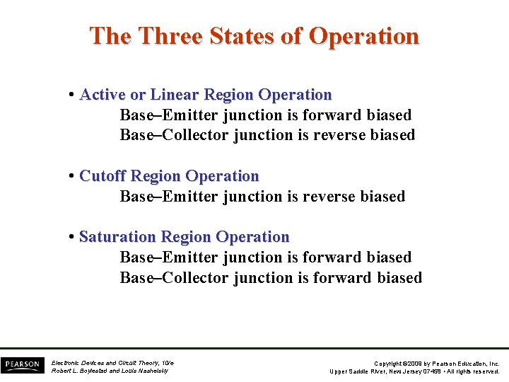
The Three States of Operation • Active or Linear Region Operation Base–Emitter junction is forward biased Base–Collector junction is reverse biased • Cutoff Region Operation Base–Emitter junction is reverse biased • Saturation Region Operation Base–Emitter junction is forward biased Base–Collector junction is forward biased Electronic Devices and Circuit Theory, 10/e Robert L. Boylestad and Louis Nashelsky Copyright © 2009 by Pearson Education, Inc. Upper Saddle River, New Jersey 07458 • All rights reserved.
DC Biasing Circuits • • • Fixed-bias circuit Emitter-stabilized bias circuit Collector-emitter loop Voltage divider bias circuit DC bias with voltage feedback Electronic Devices and Circuit Theory, 10/e Robert L. Boylestad and Louis Nashelsky Copyright © 2009 by Pearson Education, Inc. Upper Saddle River, New Jersey 07458 • All rights reserved.
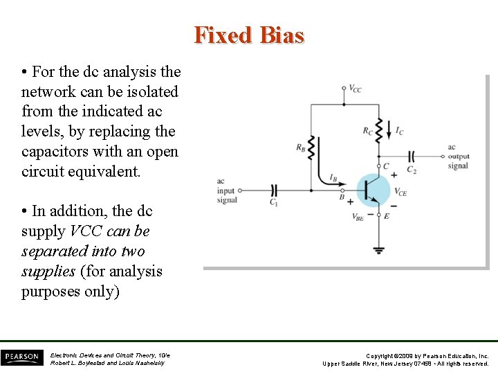
Fixed Bias • For the dc analysis the network can be isolated from the indicated ac levels, by replacing the capacitors with an open circuit equivalent. • In addition, the dc supply VCC can be separated into two supplies (for analysis purposes only) Electronic Devices and Circuit Theory, 10/e Robert L. Boylestad and Louis Nashelsky Copyright © 2009 by Pearson Education, Inc. Upper Saddle River, New Jersey 07458 • All rights reserved.
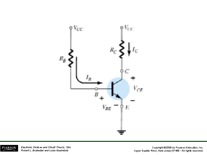
Electronic Devices and Circuit Theory, 10/e Robert L. Boylestad and Louis Nashelsky Copyright © 2009 by Pearson Education, Inc. Upper Saddle River, New Jersey 07458 • All rights reserved.
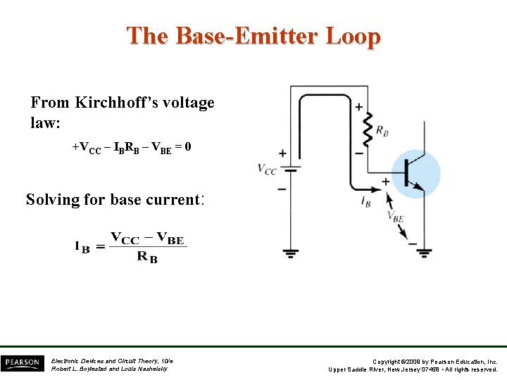
The Base-Emitter Loop From Kirchhoff’s voltage law: +VCC – IBRB – VBE = 0 Solving for base current: Electronic Devices and Circuit Theory, 10/e Robert L. Boylestad and Louis Nashelsky Copyright © 2009 by Pearson Education, Inc. Upper Saddle River, New Jersey 07458 • All rights reserved.
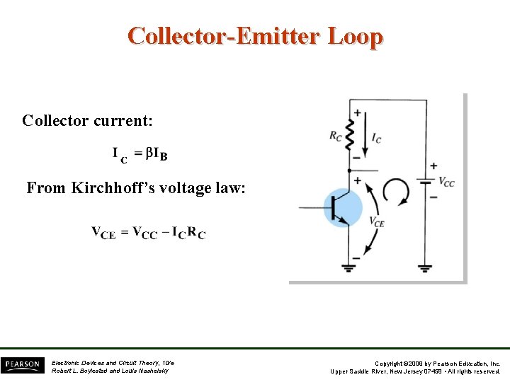
Collector-Emitter Loop Collector current: From Kirchhoff’s voltage law: Electronic Devices and Circuit Theory, 10/e Robert L. Boylestad and Louis Nashelsky Copyright © 2009 by Pearson Education, Inc. Upper Saddle River, New Jersey 07458 • All rights reserved.
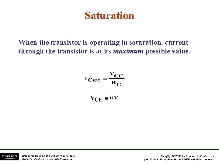
Saturation When the transistor is operating in saturation, current through the transistor is at its maximum possible value. Electronic Devices and Circuit Theory, 10/e Robert L. Boylestad and Louis Nashelsky Copyright © 2009 by Pearson Education, Inc. Upper Saddle River, New Jersey 07458 • All rights reserved.
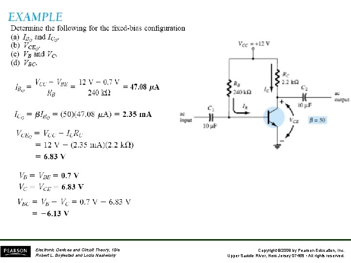
Electronic Devices and Circuit Theory, 10/e Robert L. Boylestad and Louis Nashelsky Copyright © 2009 by Pearson Education, Inc. Upper Saddle River, New Jersey 07458 • All rights reserved.
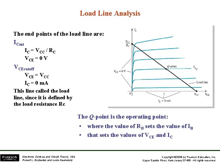
Load Line Analysis The end points of the load line are: ICsat IC = VCC / RC VCE = 0 V VCEcutoff VCE = VCC IC = 0 m. A This line called the load line, since it is defined by the load resistance Rc The Q-point is the operating point: • where the value of RB sets the value of IB • that sets the values of VCE and IC Electronic Devices and Circuit Theory, 10/e Robert L. Boylestad and Louis Nashelsky Copyright © 2009 by Pearson Education, Inc. Upper Saddle River, New Jersey 07458 • All rights reserved.
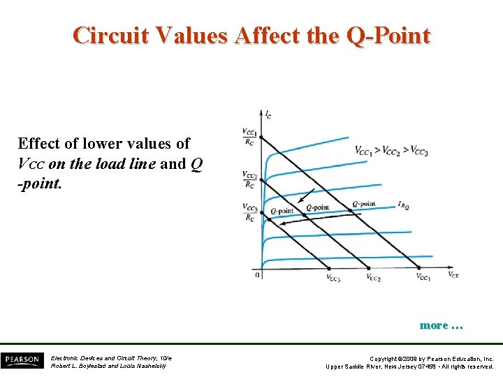
Circuit Values Affect the Q-Point Effect of lower values of VCC on the load line and Q -point. more … Electronic Devices and Circuit Theory, 10/e Robert L. Boylestad and Louis Nashelsky Copyright © 2009 by Pearson Education, Inc. Upper Saddle River, New Jersey 07458 • All rights reserved.
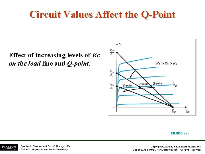
Circuit Values Affect the Q-Point Effect of increasing levels of RC on the load line and Q-point. more … Electronic Devices and Circuit Theory, 10/e Robert L. Boylestad and Louis Nashelsky Copyright © 2009 by Pearson Education, Inc. Upper Saddle River, New Jersey 07458 • All rights reserved.
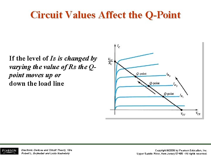
Circuit Values Affect the Q-Point If the level of IB is changed by varying the value of RB the Qpoint moves up or down the load line Electronic Devices and Circuit Theory, 10/e Robert L. Boylestad and Louis Nashelsky Copyright © 2009 by Pearson Education, Inc. Upper Saddle River, New Jersey 07458 • All rights reserved.
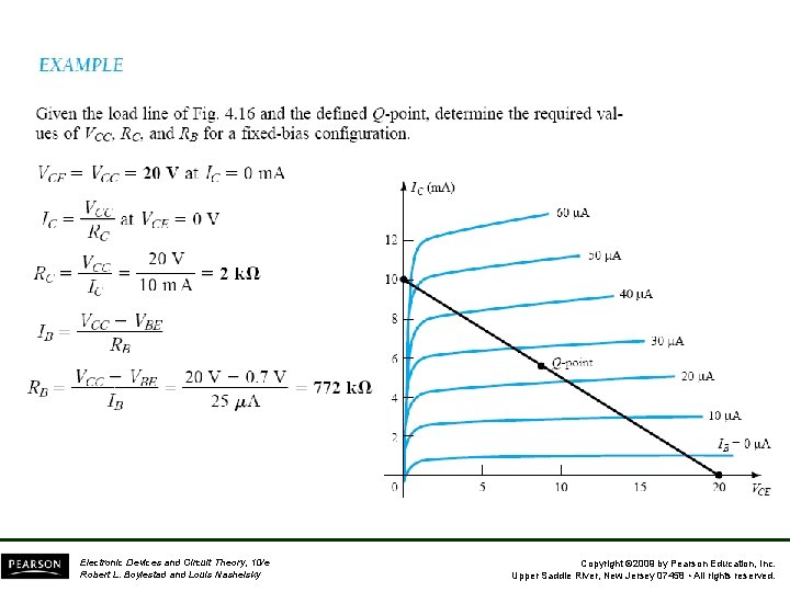
Electronic Devices and Circuit Theory, 10/e Robert L. Boylestad and Louis Nashelsky Copyright © 2009 by Pearson Education, Inc. Upper Saddle River, New Jersey 07458 • All rights reserved.
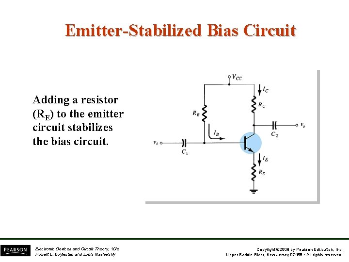
Emitter-Stabilized Bias Circuit Adding a resistor (RE) to the emitter circuit stabilizes the bias circuit. Electronic Devices and Circuit Theory, 10/e Robert L. Boylestad and Louis Nashelsky Copyright © 2009 by Pearson Education, Inc. Upper Saddle River, New Jersey 07458 • All rights reserved.
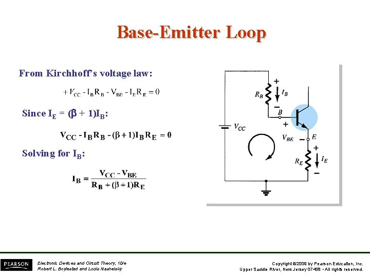
Base-Emitter Loop From Kirchhoff’s voltage law: Since IE = ( + 1)IB: Solving for IB: Electronic Devices and Circuit Theory, 10/e Robert L. Boylestad and Louis Nashelsky Copyright © 2009 by Pearson Education, Inc. Upper Saddle River, New Jersey 07458 • All rights reserved.
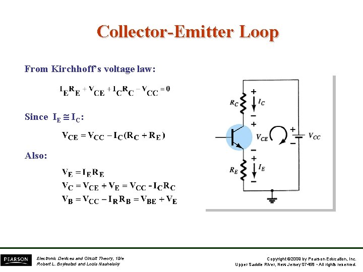
Collector-Emitter Loop From Kirchhoff’s voltage law: Since IE IC: Also: Electronic Devices and Circuit Theory, 10/e Robert L. Boylestad and Louis Nashelsky Copyright © 2009 by Pearson Education, Inc. Upper Saddle River, New Jersey 07458 • All rights reserved.
Improved Biased Stability refers to a circuit condition in which the currents and voltages will remain fairly constant over a wide range of temperatures and transistor Beta ( ) values. Adding RE to the emitter improves the stability of a transistor. The addition of the emitter resistor to the dc bias of the BJT provides improved stability, that is, the dc bias currents and voltages remain closer to where they were set by the circuit when outside conditions, such as temperature, and transistor beta change. Electronic Devices and Circuit Theory, 10/e Robert L. Boylestad and Louis Nashelsky Copyright © 2009 by Pearson Education, Inc. Upper Saddle River, New Jersey 07458 • All rights reserved.
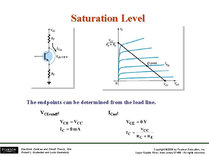
Saturation Level The endpoints can be determined from the load line. VCEcutoff: Electronic Devices and Circuit Theory, 10/e Robert L. Boylestad and Louis Nashelsky ICsat: Copyright © 2009 by Pearson Education, Inc. Upper Saddle River, New Jersey 07458 • All rights reserved.
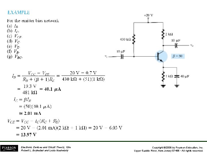
Electronic Devices and Circuit Theory, 10/e Robert L. Boylestad and Louis Nashelsky Copyright © 2009 by Pearson Education, Inc. Upper Saddle River, New Jersey 07458 • All rights reserved.
Electronic Devices and Circuit Theory, 10/e Robert L. Boylestad and Louis Nashelsky Copyright © 2009 by Pearson Education, Inc. Upper Saddle River, New Jersey 07458 • All rights reserved.
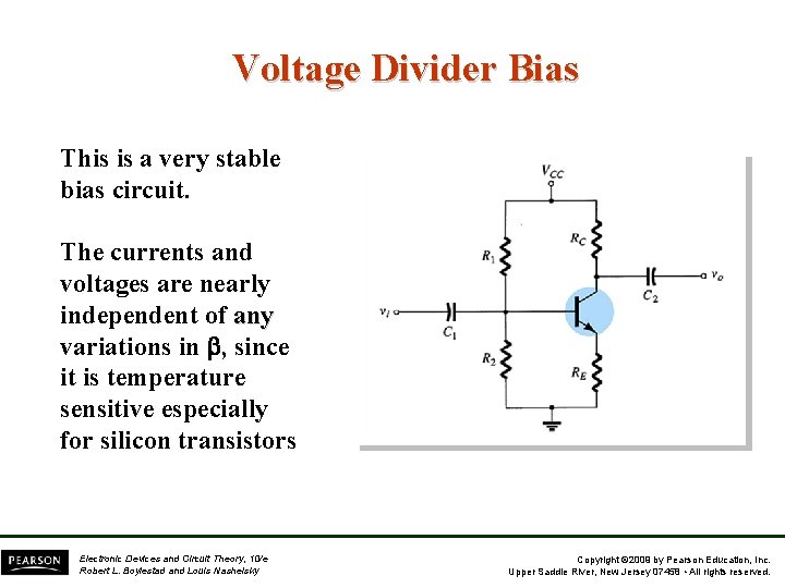
Voltage Divider Bias This is a very stable bias circuit. The currents and voltages are nearly independent of any variations in , since it is temperature sensitive especially for silicon transistors Electronic Devices and Circuit Theory, 10/e Robert L. Boylestad and Louis Nashelsky Copyright © 2009 by Pearson Education, Inc. Upper Saddle River, New Jersey 07458 • All rights reserved.
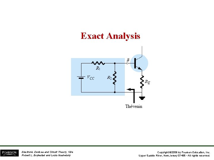
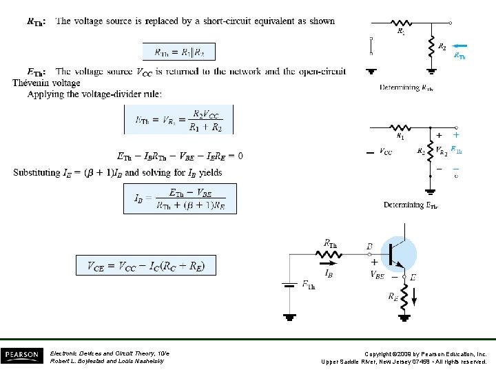
Exact Analysis Electronic Devices and Circuit Theory, 10/e Robert L. Boylestad and Louis Nashelsky Copyright © 2009 by Pearson Education, Inc. Upper Saddle River, New Jersey 07458 • All rights reserved.
Electronic Devices and Circuit Theory, 10/e Robert L. Boylestad and Louis Nashelsky Copyright © 2009 by Pearson Education, Inc. Upper Saddle River, New Jersey 07458 • All rights reserved.
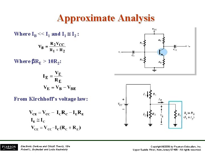
Approximate Analysis Where IB << I 1 and I 1 I 2 : Where RE > 10 R 2: From Kirchhoff’s voltage law: Electronic Devices and Circuit Theory, 10/e Robert L. Boylestad and Louis Nashelsky Copyright © 2009 by Pearson Education, Inc. Upper Saddle River, New Jersey 07458 • All rights reserved.
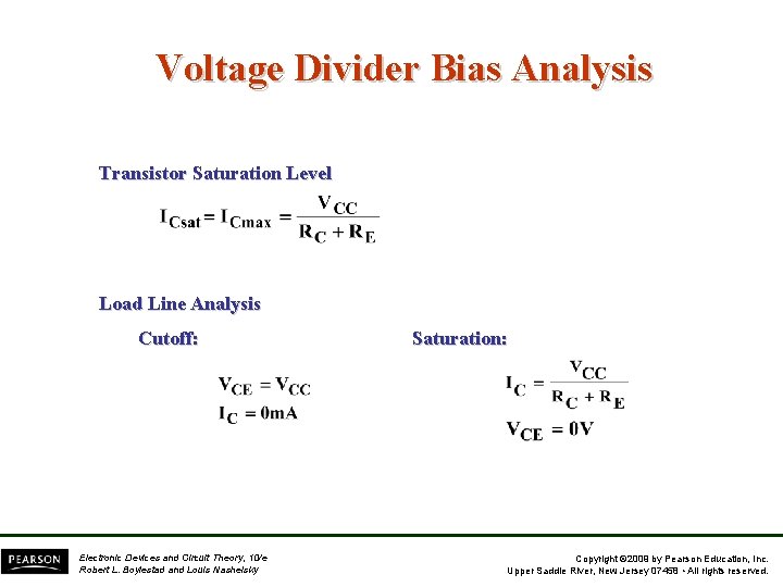
Voltage Divider Bias Analysis Transistor Saturation Level Load Line Analysis Cutoff: Electronic Devices and Circuit Theory, 10/e Robert L. Boylestad and Louis Nashelsky Saturation: Copyright © 2009 by Pearson Education, Inc. Upper Saddle River, New Jersey 07458 • All rights reserved.
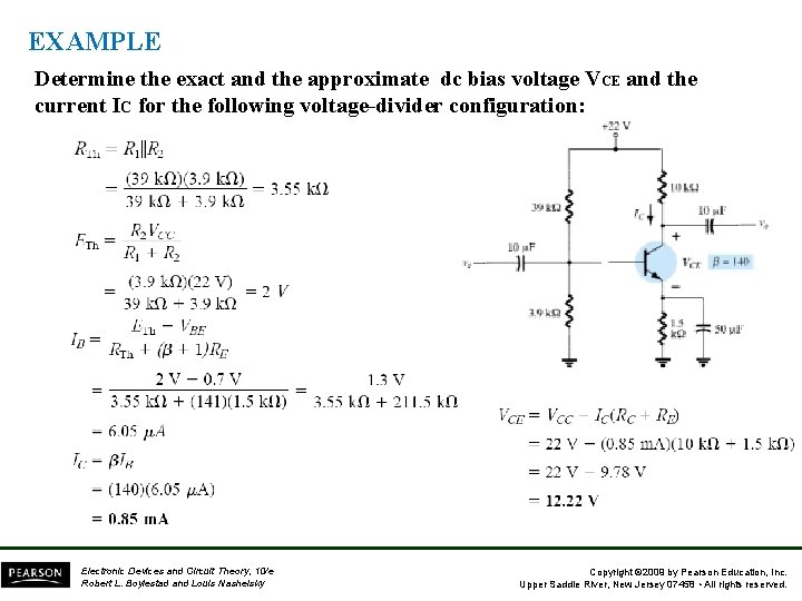
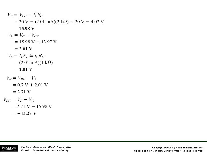
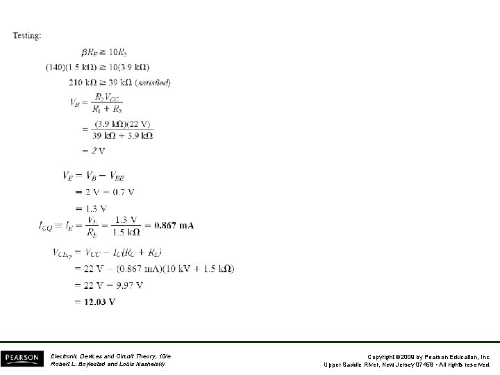
EXAMPLE Determine the exact and the approximate dc bias voltage VCE and the current IC for the following voltage-divider configuration: Electronic Devices and Circuit Theory, 10/e Robert L. Boylestad and Louis Nashelsky Copyright © 2009 by Pearson Education, Inc. Upper Saddle River, New Jersey 07458 • All rights reserved.
Electronic Devices and Circuit Theory, 10/e Robert L. Boylestad and Louis Nashelsky Copyright © 2009 by Pearson Education, Inc. Upper Saddle River, New Jersey 07458 • All rights reserved.
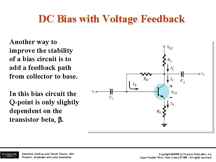
DC Bias with Voltage Feedback Another way to improve the stability of a bias circuit is to add a feedback path from collector to base. In this bias circuit the Q-point is only slightly dependent on the transistor beta, . Electronic Devices and Circuit Theory, 10/e Robert L. Boylestad and Louis Nashelsky Copyright © 2009 by Pearson Education, Inc. Upper Saddle River, New Jersey 07458 • All rights reserved.
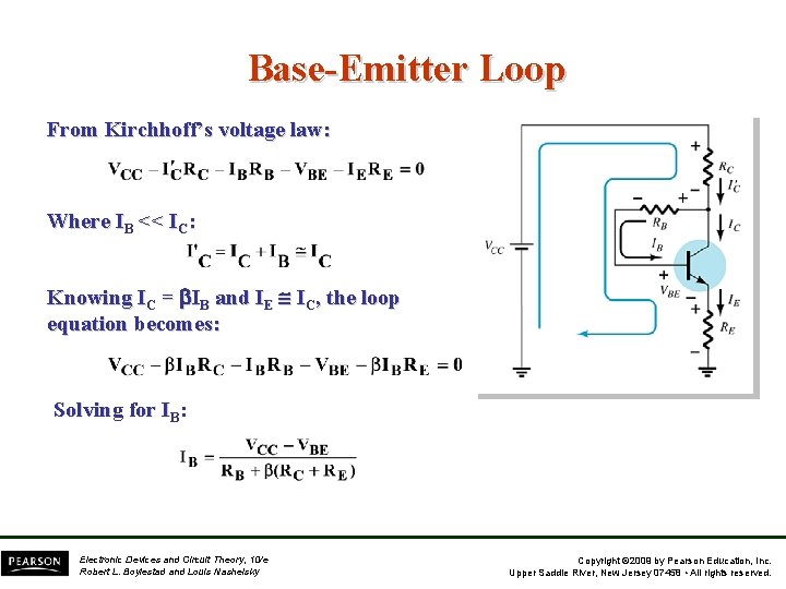
Base-Emitter Loop From Kirchhoff’s voltage law: Where IB << IC: Knowing IC = IB and IE IC, the loop equation becomes: Solving for IB: Electronic Devices and Circuit Theory, 10/e Robert L. Boylestad and Louis Nashelsky Copyright © 2009 by Pearson Education, Inc. Upper Saddle River, New Jersey 07458 • All rights reserved.
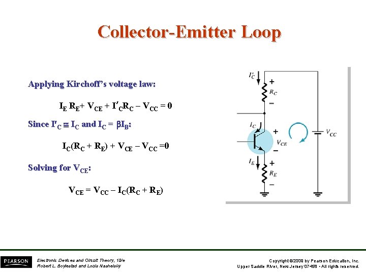
Collector-Emitter Loop Applying Kirchoff’s voltage law: IE RE+ VCE + I’CRC – VCC = 0 Since I C IC and IC = IB: IC(RC + RE) + VCE – VCC =0 Solving for VCE: VCE = VCC – IC(RC + RE) Electronic Devices and Circuit Theory, 10/e Robert L. Boylestad and Louis Nashelsky Copyright © 2009 by Pearson Education, Inc. Upper Saddle River, New Jersey 07458 • All rights reserved.
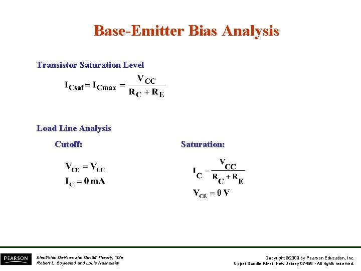
Base-Emitter Bias Analysis Transistor Saturation Level Load Line Analysis Cutoff: Electronic Devices and Circuit Theory, 10/e Robert L. Boylestad and Louis Nashelsky Saturation: Copyright © 2009 by Pearson Education, Inc. Upper Saddle River, New Jersey 07458 • All rights reserved.
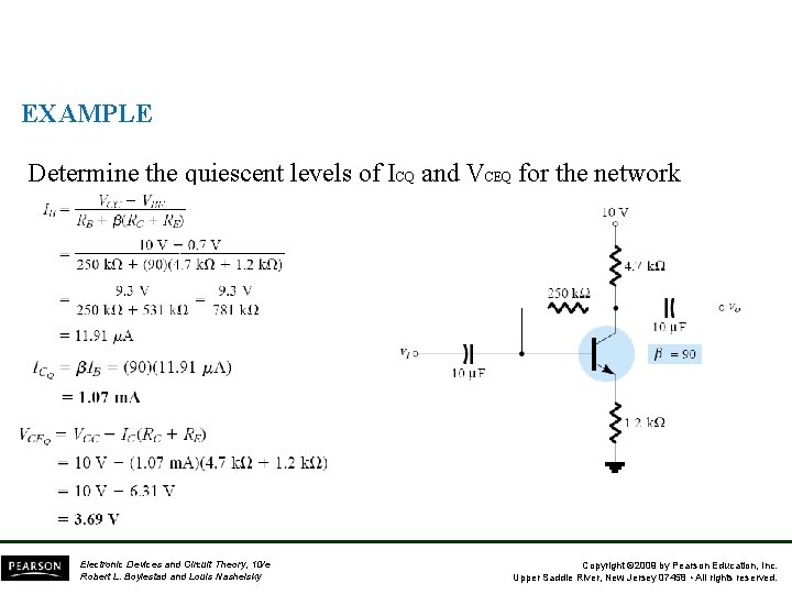
EXAMPLE Determine the quiescent levels of ICQ and VCEQ for the network Electronic Devices and Circuit Theory, 10/e Robert L. Boylestad and Louis Nashelsky Copyright © 2009 by Pearson Education, Inc. Upper Saddle River, New Jersey 07458 • All rights reserved.
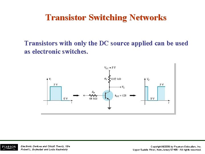
Transistor Switching Networks Transistors with only the DC source applied can be used as electronic switches. Electronic Devices and Circuit Theory, 10/e Robert L. Boylestad and Louis Nashelsky Copyright © 2009 by Pearson Education, Inc. Upper Saddle River, New Jersey 07458 • All rights reserved.
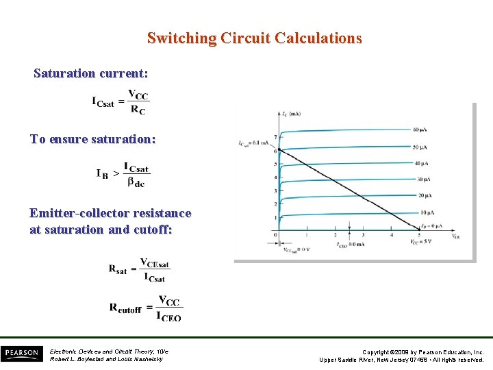
Switching Circuit Calculations Saturation current: To ensure saturation: Emitter-collector resistance at saturation and cutoff: Electronic Devices and Circuit Theory, 10/e Robert L. Boylestad and Louis Nashelsky Copyright © 2009 by Pearson Education, Inc. Upper Saddle River, New Jersey 07458 • All rights reserved.
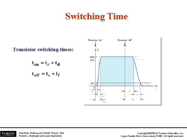
Switching Time Transistor switching times: Electronic Devices and Circuit Theory, 10/e Robert L. Boylestad and Louis Nashelsky Copyright © 2009 by Pearson Education, Inc. Upper Saddle River, New Jersey 07458 • All rights reserved.
PNP Transistors The analysis for pnp transistor biasing circuits is the same as that for npn transistor circuits. The only difference is that the currents are flowing in the opposite direction. Electronic Devices and Circuit Theory, 10/e Robert L. Boylestad and Louis Nashelsky Copyright © 2009 by Pearson Education, Inc. Upper Saddle River, New Jersey 07458 • All rights reserved.
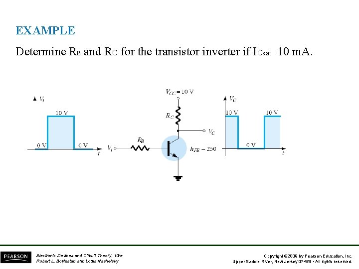
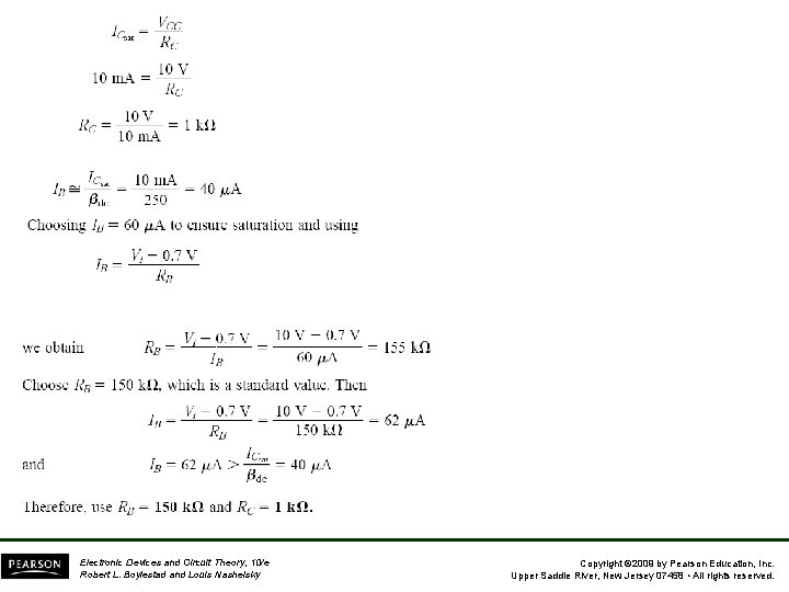
EXAMPLE Determine RB and RC for the transistor inverter if ICsat 10 m. A. Electronic Devices and Circuit Theory, 10/e Robert L. Boylestad and Louis Nashelsky Copyright © 2009 by Pearson Education, Inc. Upper Saddle River, New Jersey 07458 • All rights reserved.
Electronic Devices and Circuit Theory, 10/e Robert L. Boylestad and Louis Nashelsky Copyright © 2009 by Pearson Education, Inc. Upper Saddle River, New Jersey 07458 • All rights reserved.
- Slides: 43