Chapter 4 Combinational Logic Functions and Circuits Page
Chapter 4 Combinational Logic Functions and Circuits Page
Functional Blocks · Essential in understanding computer design since used in many places · · Code Converters Decoders Multiplexers Demultiplexers and Encoders 2
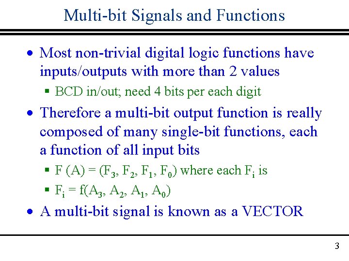
Multi-bit Signals and Functions · Most non-trivial digital logic functions have inputs/outputs with more than 2 values § BCD in/out; need 4 bits per each digit · Therefore a multi-bit output function is really composed of many single-bit functions, each a function of all input bits § F (A) = (F 3, F 2, F 1, F 0) where each Fi is § Fi = f(A 3, A 2, A 1, A 0) · A multi-bit signal is known as a VECTOR 3
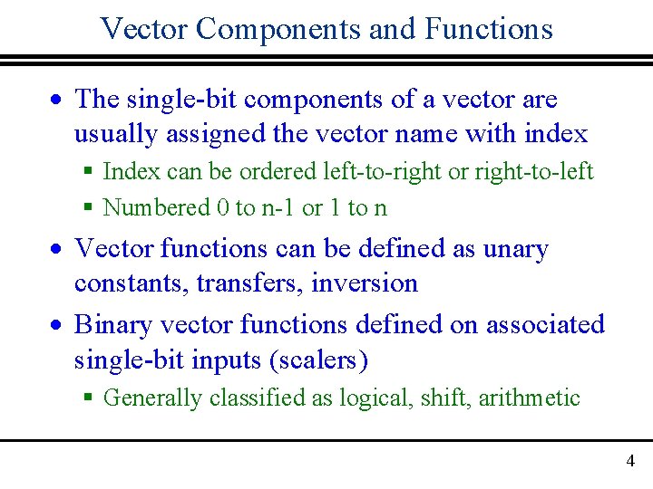
Vector Components and Functions · The single-bit components of a vector are usually assigned the vector name with index § Index can be ordered left-to-right or right-to-left § Numbered 0 to n-1 or 1 to n · Vector functions can be defined as unary constants, transfers, inversion · Binary vector functions defined on associated single-bit inputs (scalers) § Generally classified as logical, shift, arithmetic 4
Enabling · Enable signals permit or prevent something from occuring (a control signal) § State is described as either: w Active - ON or Enabled w Passive - OFF or Disabled § Polarity of control state can be: w Active high - schematic symbol doesn’t have bubble w Active low - Schematic symbol has bubble · A single enable signal may control vector operations (e. g. multi-bit 3 -state buffer) 5
Decoders/Demultiplexers · A Decoder converts n-bit coded information 2 n distinct outputs(n inputs, 2 n outputs). · Only one of the outputs, the one with index corresponding to the input is 1 and all others are zero. Generated outputs are actually ‘minterms’ of the inputs. Example: 3 to 8 decoder has 3 inputs (A 0, A 1, A 2) and 8 outputs D 0, D 1, ……. D 7 If the input is 101, output is: 00000100 6

Decoders 7
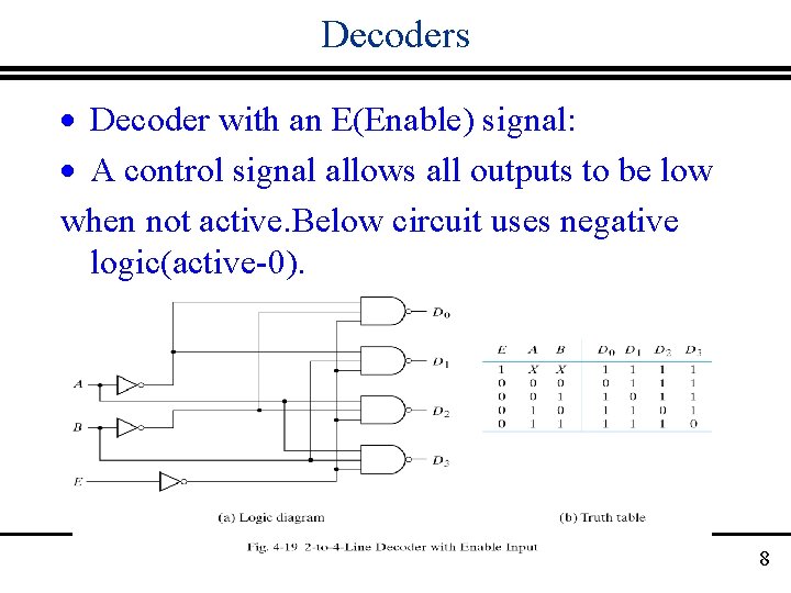
Decoders · Decoder with an E(Enable) signal: · A control signal allows all outputs to be low when not active. Below circuit uses negative logic(active-0). 8
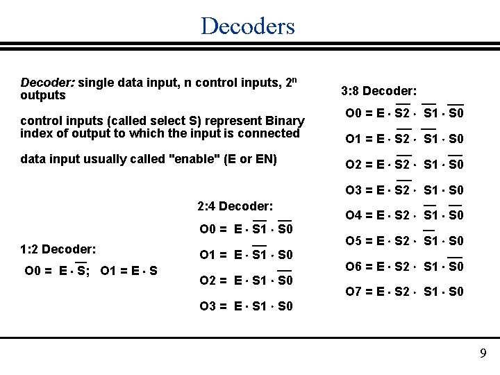
Decoders Decoder: single data input, n control inputs, 2 n outputs control inputs (called select S) represent Binary index of output to which the input is connected data input usually called "enable" (E or EN) 3: 8 Decoder: O 0 = E S 2 S 1 S 0 O 1 = E S 2 S 1 S 0 O 2 = E S 2 S 1 S 0 O 3 = E S 2 S 1 S 0 2: 4 Decoder: O 0 = E S 1 S 0 1: 2 Decoder: O 0 = E S; O 1 = E S 1 S 0 O 2 = E S 1 S 0 O 3 = E S 1 S 0 O 4 = E S 2 S 1 S 0 O 5 = E S 2 S 1 S 0 O 6 = E S 2 S 1 S 0 O 7 = E S 2 S 1 S 0 9
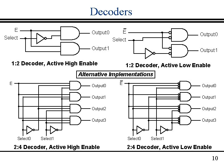
Decoders E E Output 0 Select Output 1 1: 2 Decoder, Active High Enable 1: 2 Decoder, Active Low Enable Alternative Implementations E Output 0 Select 0 E Output 0 Output 1 Output 2 Output 3 Select 1 2: 4 Decoder, Active High Enable Select 0 Select 1 2: 4 Decoder, Active Low Enable 10
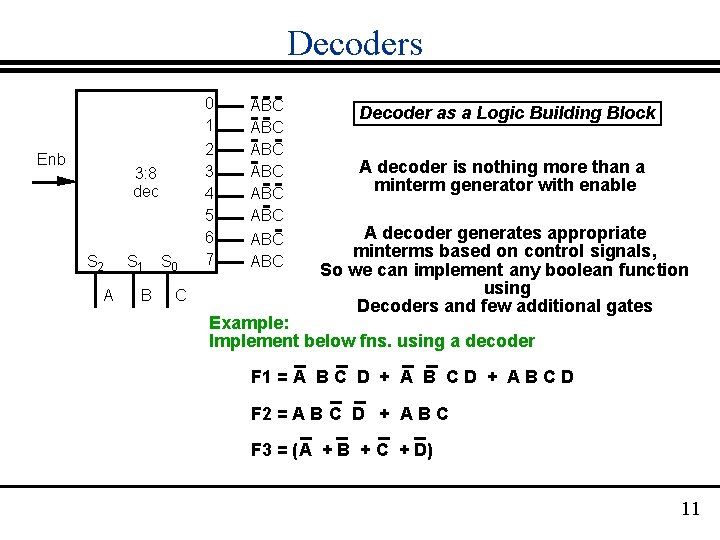
Decoders Enb 3: 8 dec S 2 A S 1 B S 0 C 0 1 2 3 4 5 6 7 ABC ABC Decoder as a Logic Building Block A decoder is nothing more than a minterm generator with enable A decoder generates appropriate minterms based on control signals, So we can implement any boolean function using Decoders and few additional gates Example: Implement below fns. using a decoder F 1 = A B C D + A B C D F 2 = A B C D + A B C F 3 = (A + B + C + D) 11
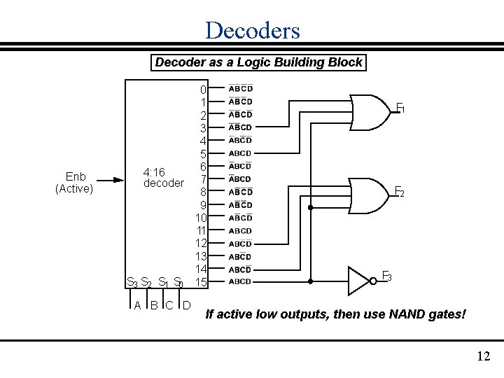
Decoders Decoder as a Logic Building Block Enb (Active) 0 1 2 3 4 5 6 4: 16 decoder 7 8 9 10 11 12 13 14 S 3 S 2 S 1 S 0 15 A B C D F 1 F 2 F 3 If active low outputs, then use NAND gates! 12
Decoders · Hierarchical Design: We want to obtain a 4 x 16 decoder using 3 x 8 decoders with enable inputs. · How many do we need? 13
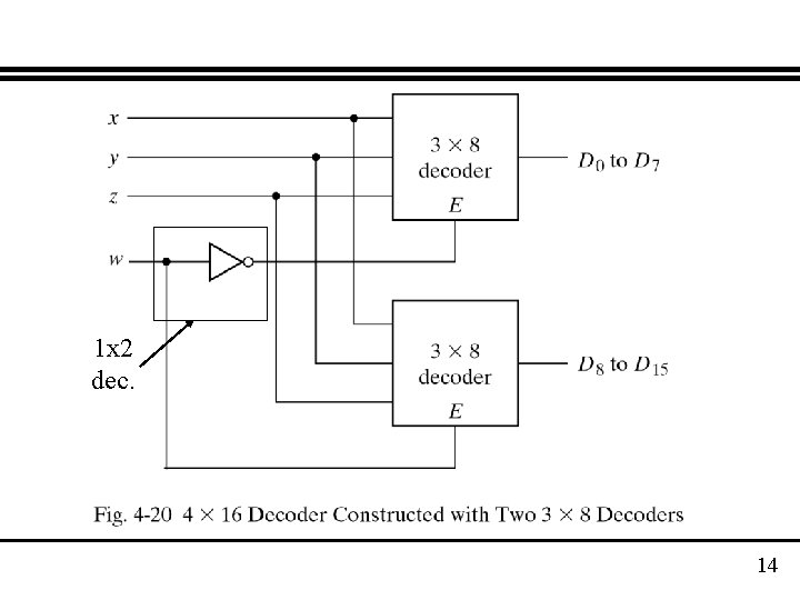
1 x 2 dec. 14
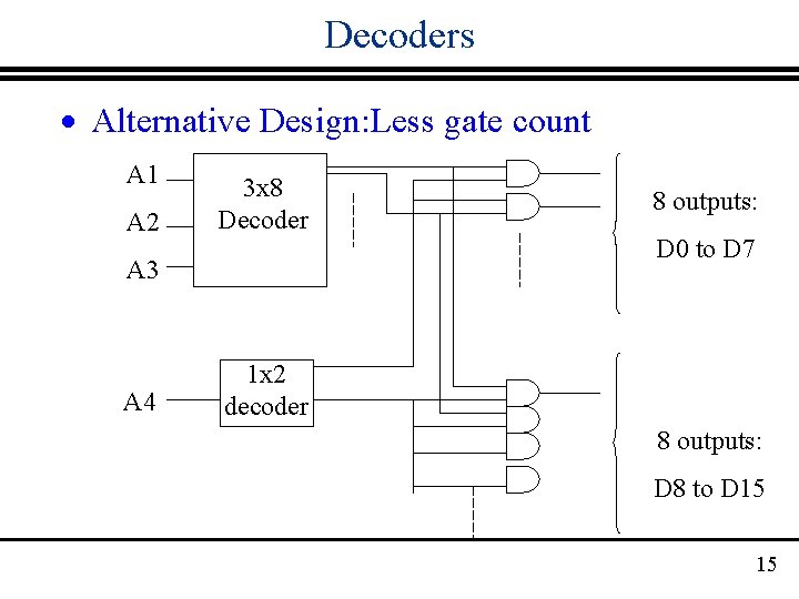
Decoders · Alternative Design: Less gate count A 1 A 2 3 x 8 Decoder A 3 A 4 8 outputs: D 0 to D 7 1 x 2 decoder 8 outputs: D 8 to D 15 15
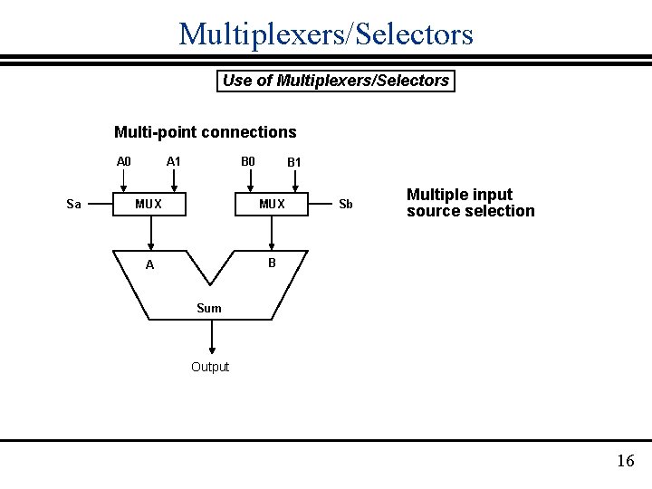
Multiplexers/Selectors Use of Multiplexers/Selectors Multi-point connections A 0 Sa A 1 B 0 B 1 MUX A B Sb Multiple input source selection Sum Output 16
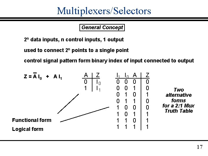
Multiplexers/Selectors General Concept 2 n data inputs, n control inputs, 1 output used to connect 2 n points to a single point control signal pattern form binary index of input connected to output Z = A I 0 + A I 1 Functional form Logical form A 0 1 Z I 0 I 1 0 0 1 1 I 0 0 0 1 1 A 0 1 0 1 Z 0 0 1 1 1 Two alternative forms for a 2: 1 Mux Truth Table 17
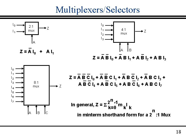
Multiplexers/Selectors I 0 I 1 2: 1 mux I 0 I 1 I 2 I 3 Z A 4: 1 mux A Z = A I 0 + A I 1 Z B Z = A B I 0 + A B I 1 + A B I 2 + A B I 3 I 0 I 1 I 2 I 3 8: 1 mux I 4 I 5 I 6 I 7 Z Z = A B C I 0 + A B C I 1 + A B C I 2 + A B C I 3 + A B C I 4 + A B C I 5 + A B C I 6 + A B C I 7 n -1 2 In general, Z = m I k=0 k k A B C n in minterm shorthand form for a 2 : 1 Mux 18
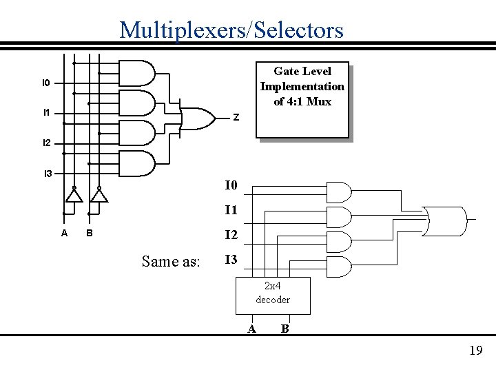
Multiplexers/Selectors Gate Level Implementation of 4: 1 Mux I 0 I 1 Z I 2 I 3 I 0 I 1 A I 2 B Same as: I 3 2 x 4 decoder A B 19
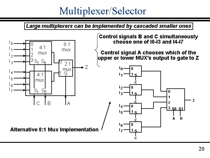
Multiplexer/Selector Large multiplexers can be implemented by cascaded smaller ones I 0 I 1 I 2 I 3 I 4 I 5 I 6 I 7 0 1 4: 1 2 mux 3 S 1 S 0 Control signals B and C simultaneously choose one of I 0 -I 3 and I 4 -I 7 8: 1 mux 0 2: 1 mux 1 S 4: 1 mux Control signal A chooses which of the upper or lower MUX's output to gate to Z Z 0 I 1 1 S C S 1 S 0 C I 0 B A I 2 0 I 3 1 S 0 C 2 I 4 0 I 5 1 S C Alternative 8: 1 Mux Implementation I 6 0 I 7 1 S 1 Z 3 S 0 S 1 A B C 20
Multiplexers/Selectors · Multiplexers also can be used in boolean function implementation Example: Assume the inputs are A, B, C and F= m 1+m 3+m 5 and we have a 8 x 1 mux. Now use: · the select lines of the mux as A, B, C · The input lines as 0 or 1 , 1’s corresponding to nonzero minterms of F, that is, I 1, I 3, I 5 in this case 21
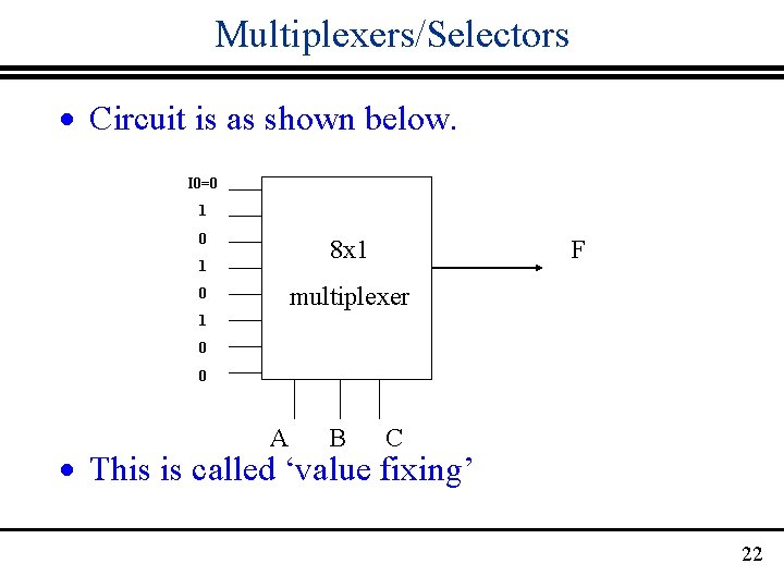
Multiplexers/Selectors · Circuit is as shown below. I 0=0 1 0 8 x 1 1 F multiplexer 0 1 0 0 A B C · This is called ‘value fixing’ 22
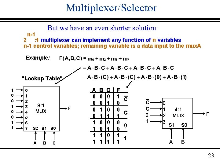
Multiplexer/Selector But we have an even shorter solution: n-1 2 : 1 multiplexer can implement any function of n variables n-1 control variables; remaining variable is a data input to the mux. A Example: "Lookup Table" 1 0 0 1 1 0 1 2 3 4 5 6 7 8: 1 MUX F S 2 S 1 S 0 A B C A 0 0 1 1 B 0 0 1 1 C 0 1 0 1 F 1 0 0 1 1 C C 0 1 0 1 2 3 4: 1 MUX S 1 S 0 A B F 23
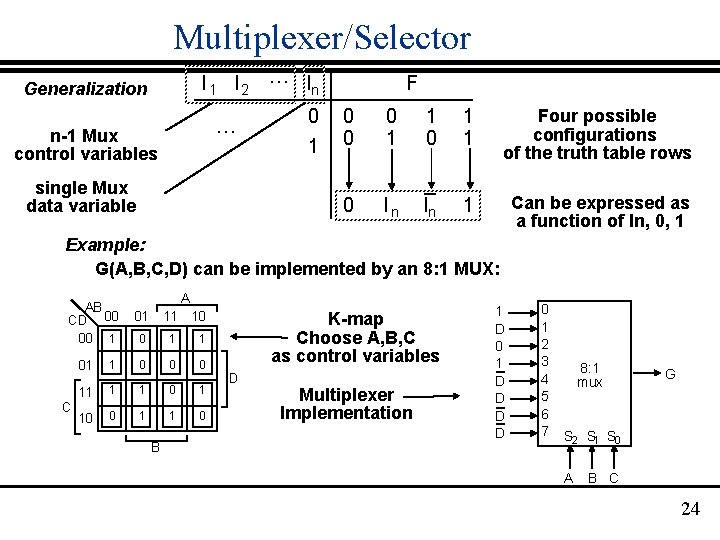
Multiplexer/Selector I 1 I 2 … In Generalization … n-1 Mux control variables single Mux data variable 0 1 F 0 0 0 1 1 Four possible configurations of the truth table rows 0 In In 1 Can be expressed as a function of In, 0, 1 Example: G(A, B, C, D) can be implemented by an 8: 1 MUX: AB CD 00 00 1 C A 01 11 10 0 1 1 0 0 0 11 1 1 0 1 10 0 1 1 0 B K-map Choose A, B, C as control variables D Multiplexer Implementation 1 D 0 1 D D 0 1 2 3 4 5 6 7 8: 1 mux G S 2 S 1 S 0 A B C 24
Multiplexer/Selector · Multi-output multiplexers: · Assume you have 2 four-bit words A, B where · A= (A 0, A 1, A 2, A 3) · Now we want to choose only one of these words, that is one of A , B. When S=1 A should be selected. · The output will have a 4 element vector 25
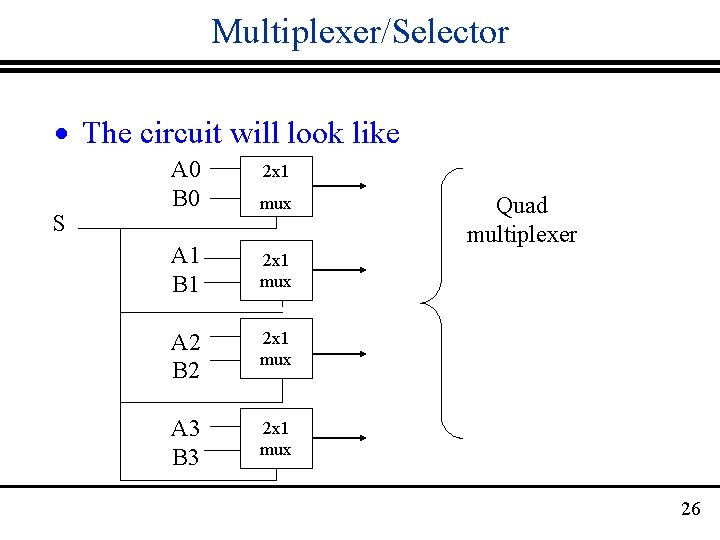
Multiplexer/Selector · The circuit will look like S A 0 B 0 mux A 1 B 1 2 x 1 mux A 2 B 2 2 x 1 mux A 3 B 3 2 x 1 mux 2 x 1 Quad multiplexer 26
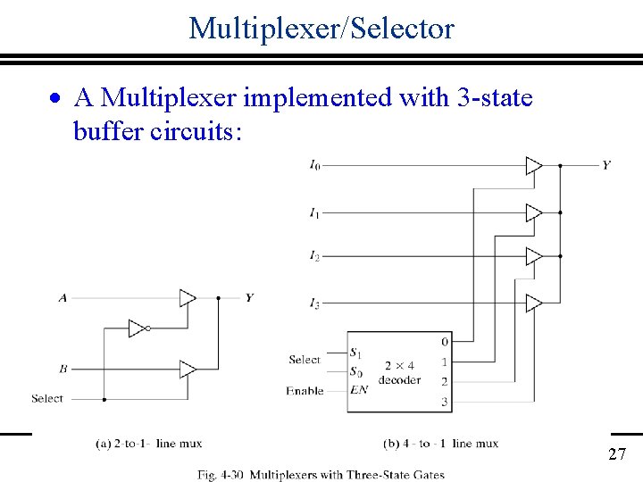
Multiplexer/Selector · A Multiplexer implemented with 3 -state buffer circuits: 27
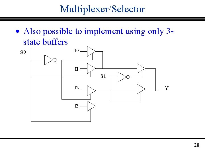
Multiplexer/Selector · Also possible to implement using only 3 state buffers S 0 I 1 S 1 I 2 Y I 3 28
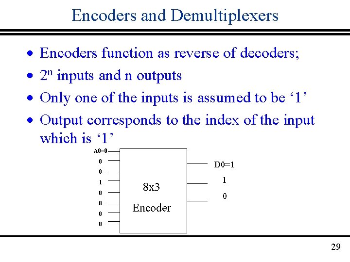
Encoders and Demultiplexers · · Encoders function as reverse of decoders; 2 n inputs and n outputs Only one of the inputs is assumed to be ‘ 1’ Output corresponds to the index of the input which is ‘ 1’ A 0=0 0 D 0=1 0 0 0 8 x 3 1 0 Encoder 0 29
Encoders and Demultiplexers · A Priority Encoder: Input can be anything. Output corresponds to the input that is a first ‘ 1’in descending order. We call it ‘priority’. · Useful in servicing input/output devices in an order of priority. Some devices like a disk need faster service. · A demultiplexer does the reverse of a multiplexer 30
- Slides: 30