CHAPTER 3 THE SEMICONDUCTOR IN EQUILIBRIUM DMT 234
CHAPTER 3 THE SEMICONDUCTOR IN EQUILIBRIUM DMT 234 SEMICONDUCTOR PHYSICS &
CONTENTS § § § Semiconductor. Thermal Equilibrium. Charge Carriers In Semiconductors. Density Of States Function (DOS) And Fermi Dirac Probability Function. The Intrinsic Carrier Concentration. Position Of Fermi Level For Intrinsic Semiconductor. Dopant Atoms And Energy Levels. The Extrinsic Semiconductor. Degenerate & Non-degenerate Semiconductors. Complete Ionization. Charge Neutrality. Position of Fermi Energy Level.
SEMICONDUCTOR § The advent of the semiconductor has revolutionized our lives, since it is the basis of all integrated circuits and microprocessors. § To distinguish between the electrical properties of materials we can group them into three (3) sections : 1. Conductors. 2. Semiconductors. 3. Insulators. § The important difference between conductors, semiconductors and insulators lies in the number of free electrons present in the material. § Perhaps the best way to consider the differences between them is to use the band theory of solids. § As you may know, electrons in an individual atom are restricted to welldefined energy levels and energy changes within the atom only take place between one level and another.
SEMICONDUCTOR § In a solid the atoms are linked together and the electrons can occupy a whole series of energy levels grouped into bands. § The difference in energy between levels within the band is very small compared with the energy gap between the bands. § The electrical differences between one type of solid another lie in the different arrangements of the bands.
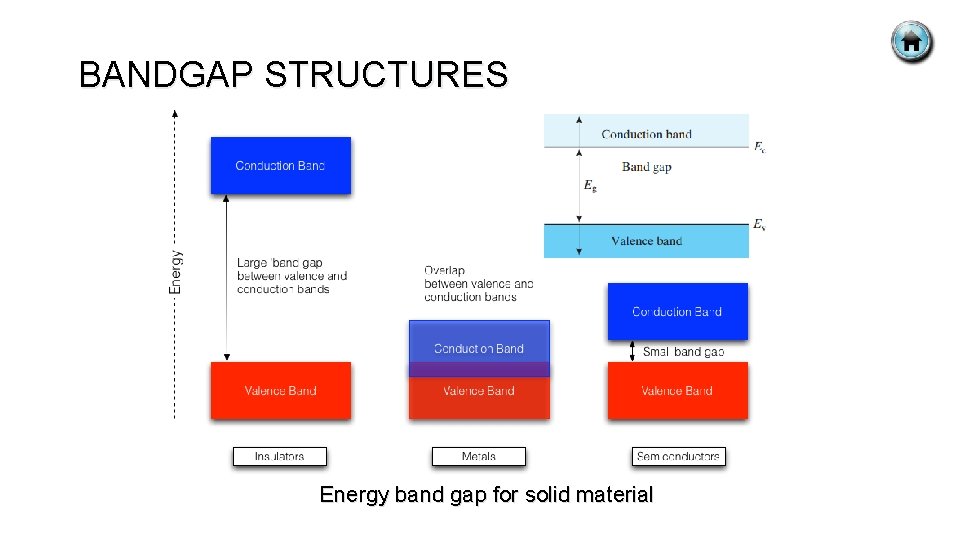
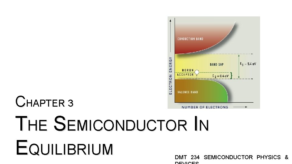
BANDGAP STRUCTURES Energy band gap for solid material
INTRINSIC SEMICONDUCTOR § In semiconductors and insulators, when an external electric field is applied the conduction is not possible as there is a forbidden gap, which is absent in metals. § In order to conduct, the electrons from the top of the full valence band have to move into the conduction band, by crossing the forbidden gap. Eg: Si where the forbidden gap is about 1 e. V. § The field that needs to be applied to do this work will be extremely large. § The distance between these two locations is about 1Å (10 10 m). § A field gradient of approximately 1 V/ (10 10 m) = 1010 Vm 1 is necessary to move an electron from the top of the valence band to the bottom of the conduction band. § The other possibility by which this transition can be brought about is by thermal excitation. § At room temperature, thermal energy that is available can excite a limited number of electrons across the energy gap. This limited number accounts for semi-conduction.
INTRINSIC SEMICONDUCTOR § When the energy gap is large as in diamond, the number of electrons that can be excited across the gap is extremely small. § In intrinsic semiconductors, the conduction is due to the intrinsic processes (without the influence of impurities). § A pure crystal of silicon or germanium is an intrinsic semiconductor. The electrons that are excited from the top of the valence band to the bottom of the conduction band by thermal energy are responsible for conduction. § The number of electrons excited across the gap can be calculated from the Fermi-Dirac probability distribution.
THERMAL EQUILIBRIUM § Equilibrium : § No external forces such as voltages, electric fields, magnetic fields or temperature gradients are acting on the semiconductor. § No external forces are applied : § Electric field = 0. § Magnetic field = 0. § Mechanical stress = 0. § No light. § Dynamic situation in which every process is balanced by its inverse process : § Electron-hole pair (EHP) generation rate = EHP recombination rate. § Thermal agitation : § Electrons and holes exchange energy with the crystal lattice and each other. § Every energy state in the conduction band valence band has a
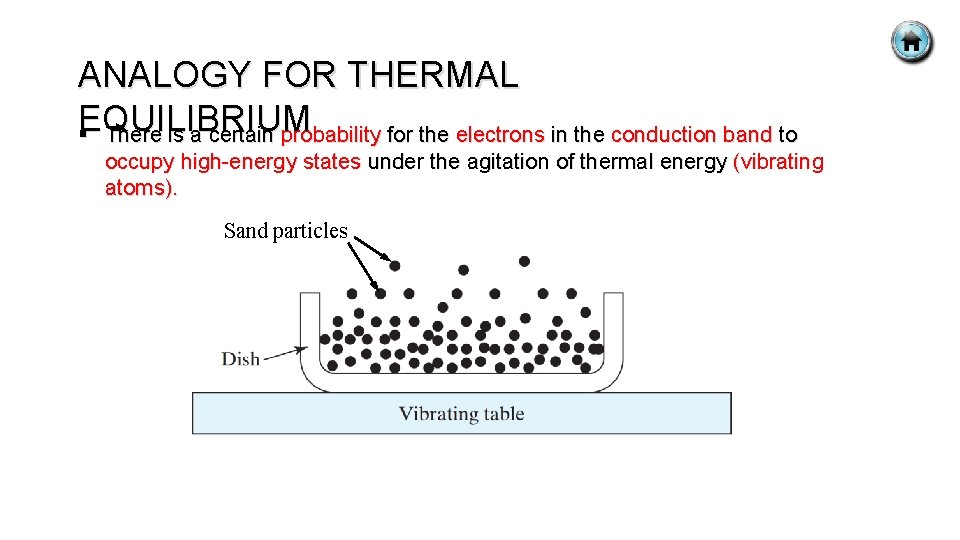
ANALOGY FOR THERMAL EQUILIBRIUM § There is a certain probability for the electrons in the conduction band to occupy high-energy states under the agitation of thermal energy (vibrating atoms). Sand particles
CHARGE CARRIERS IN SEMICONDUCTORS § Charge carrier (electron and hole) can contribute to a current. § Current is determined by the number of electrons in conduction band number of holes in valence band. § Important characteristics : § Density of these charge carriers. § It is related to density of states function and Fermi distribution function. § Density of states (DOS) tells us how many states exist at a given energy E. § The Fermi distribution function f(E) specifies how many of the existing states at the energy E will be filled with electrons.
NUMBER OF CARRIERS (n) § How to count number of carriers, n? § Assumption : § Pauli exclusion principle. § If we know : 1. No. of energy states → Density of states (DOS). 2. Occupied energy states → The probability that energy states is occupied “Fermi-Dirac distribution function”. n(E) = DOS x “Fermi-Dirac distribution function”
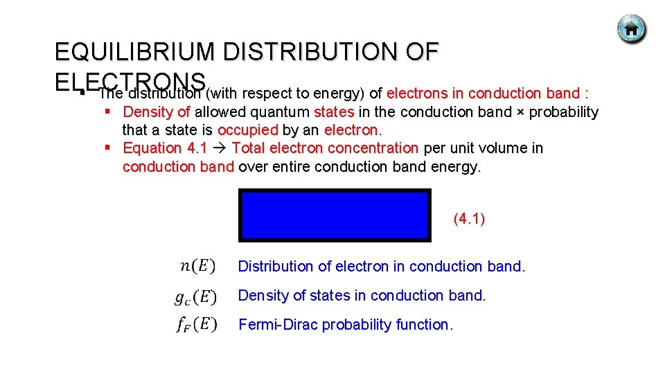
EQUILIBRIUM DISTRIBUTION OF ELECTRONS § The distribution (with respect to energy) of electrons in conduction band : § Density of allowed quantum states in the conduction band × probability that a state is occupied by an electron. § Equation 4. 1 Total electron concentration per unit volume in conduction band over entire conduction band energy. (4. 1) Distribution of electron in conduction band. Density of states in conduction band. Fermi-Dirac probability function.
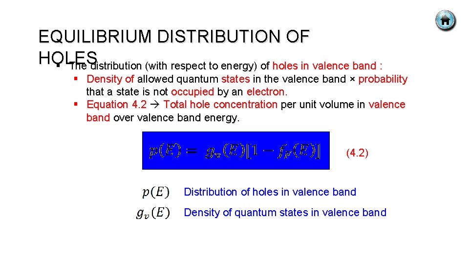
EQUILIBRIUM DISTRIBUTION OF HOLES § The distribution (with respect to energy) of holes in valence band : § Density of allowed quantum states in the valence band × probability that a state is not occupied by an electron. § Equation 4. 2 Total hole concentration per unit volume in valence band over valence band energy. (4. 2) Distribution of holes in valence band Density of quantum states in valence band
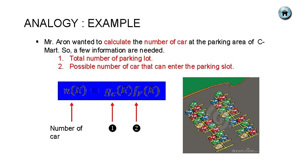
ANALOGY : EXAMPLE § Mr. Aron wanted to calculate the number of car at the parking area of CMart. So, a few information are needed. 1. Total number of parking lot. 2. Possible number of car that can enter the parking slot. Number of car ❶ ❷
THERMAL EQUILIBRIUM DISTRIBUTION OF CARRIE § In order to find thermal equilibrium electron and hole concentration determine the position of Fermi energy, EF. § Lets consider an ideal intrinsic semiconductor with no impurity atoms and no lattice defects in crystal. § At ( T=0 K ), all energy states in the valence band are filled with electrons and all energy states in conduction band are empty of electrons. § The Fermi energy lies somewhere between Ec and Ev. § As temperature increases above 0 K, the valence electrons gain thermal energy. § Few electrons in valence band may gain sufficient energy to jump to the conduction band. § Electron jumped in the conduction band hole is created in valence band. § In intrinsic semiconductor, electrons and holes are created in pairs by thermal energy. § The number of electrons in conduction band is equal to the number of
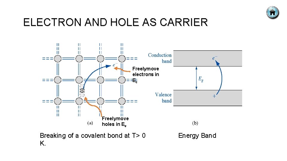
ELECTRON AND HOLE AS CARRIER Freelymove electrons in Ec Freelymove holes in Ev Breaking of a covalent bond at T> 0 K. Energy Band
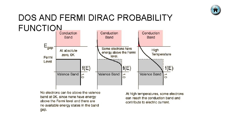
DOS AND FERMI DIRAC PROBABILITY FUNCTION
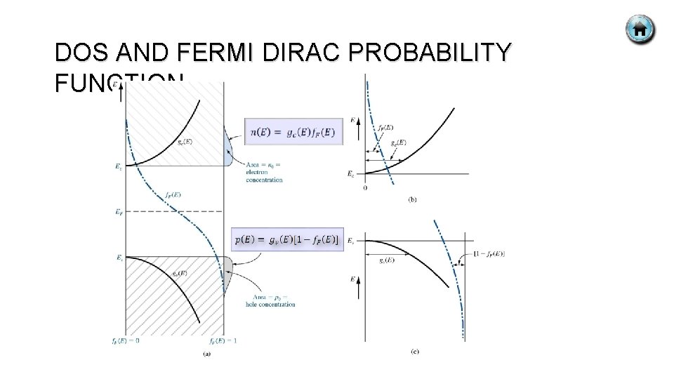
DOS AND FERMI DIRAC PROBABILITY FUNCTION
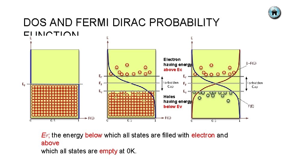
DOS AND FERMI DIRAC PROBABILITY FUNCTION Electron having energy above Ec Holes having energy below Ev EF; the energy below which all states are filled with electron and above which all states are empty at 0 K.
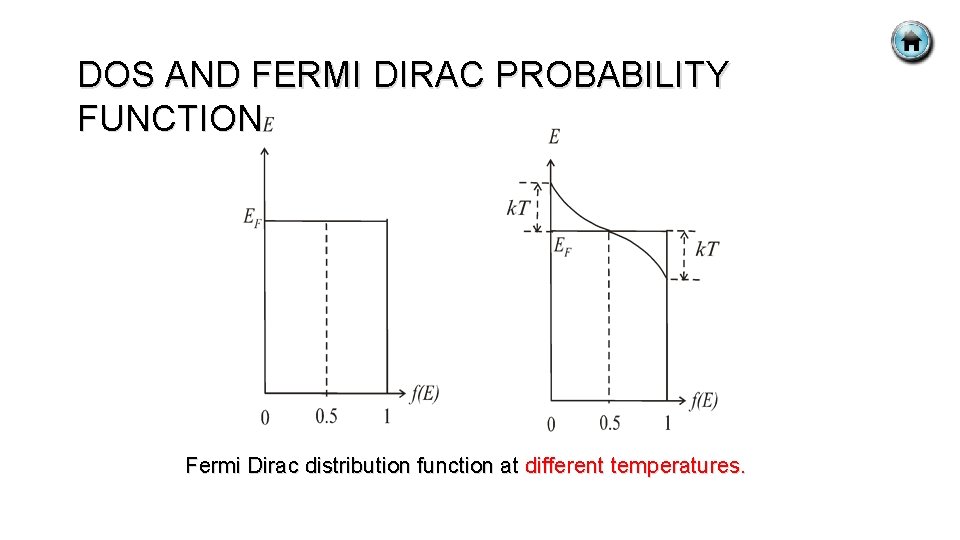
DOS AND FERMI DIRAC PROBABILITY FUNCTION Fermi Dirac distribution function at different temperatures.
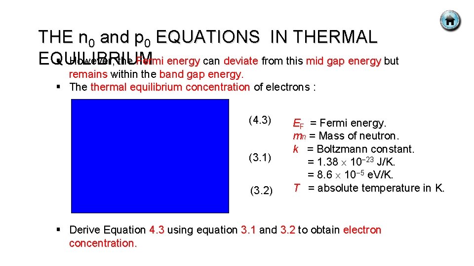
THE n 0 and p 0 EQUATIONS IN THERMAL EQUILIBRIUM § However, the Fermi energy can deviate from this mid gap energy but remains within the band gap energy. § The thermal equilibrium concentration of electrons : (4. 3) (3. 1) (3. 2) EF = Fermi energy. mn = Mass of neutron. k = Boltzmann constant. = 1. 38 10 23 J/K. = 8. 6 10 5 e. V/K. T = absolute temperature in K. § Derive Equation 4. 3 using equation 3. 1 and 3. 2 to obtain electron concentration.
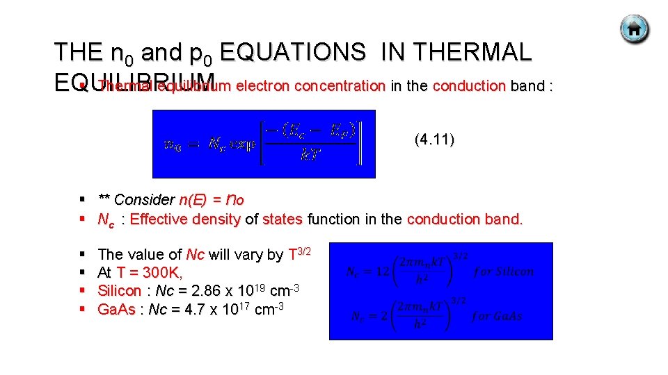
THE n 0 and p 0 EQUATIONS IN THERMAL EQUILIBRIUM § Thermal equilibrium electron concentration in the conduction band : (4. 11) § § ** Consider n(E) = no Nc : Effective density of states function in the conduction band. § § The value of Nc will vary by T 3/2 At T = 300 K, Silicon : Nc = 2. 86 x 1019 cm-3 Ga. As : Nc = 4. 7 x 1017 cm-3
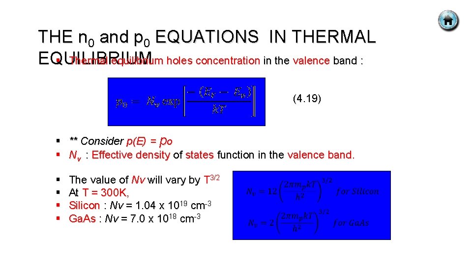
THE n 0 and p 0 EQUATIONS IN THERMAL EQUILIBRIUM § Thermal equilibrium holes concentration in the valence band : (4. 19) § § ** Consider p(E) = po Nv : Effective density of states function in the valence band. § § The value of Nv will vary by T 3/2 At T = 300 K, Silicon : Nv = 1. 04 x 1019 cm-3 Ga. As : Nv = 7. 0 x 1018 cm-3
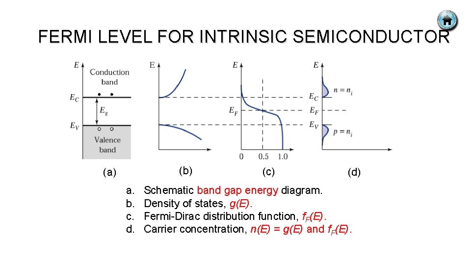
FERMI LEVEL FOR INTRINSIC SEMICONDUCTOR (b) (a) a. b. c. d. (c) (d) Schematic band gap energy diagram. Density of states, g(E). Fermi-Dirac distribution function, f. F(E). Carrier concentration, n(E) = g(E) and f. F(E).
INTRINSIC CARRIER CONCENTRATION
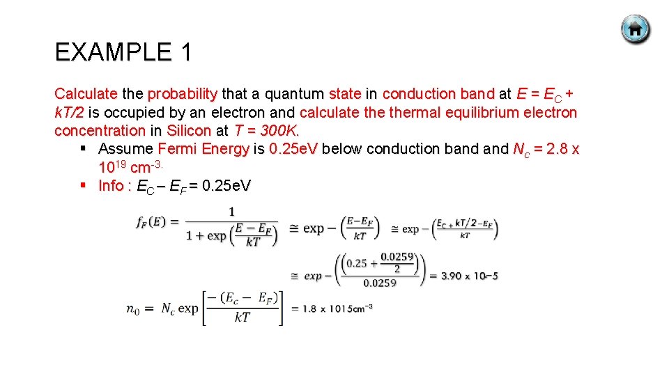
EXAMPLE 1 Calculate the probability that a quantum state in conduction band at E = EC + k. T/2 is occupied by an electron and calculate thermal equilibrium electron concentration in Silicon at T = 300 K. § Assume Fermi Energy is 0. 25 e. V below conduction band Nc = 2. 8 x 1019 cm-3. § Info : EC – EF = 0. 25 e. V

EXAMPLE 2 Calculate thermal equilibrium hole concentration in silicon at T= 400 K. Assume that the Fermi energy is 0. 27 e. V above the valence band energy. The value of Nv for silicon at T = 300 K is 1. 04 x 1019 cm-3. The Nv is vary as T 3/2. § Info : § EF – EV = 0. 27 e. V § k. T = (0. 0259)(400/300) = 0. 03453 e. V § NV = (1. 04 x 1019)(400/300)3/2 = 1. 6 x 1019 cm-3 (4. 19) § Answer : PO = 6. 43 x 1015 cm-3
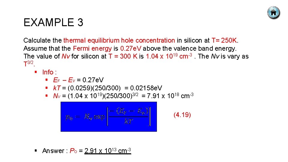
EXAMPLE 3 Calculate thermal equilibrium hole concentration in silicon at T= 250 K. Assume that the Fermi energy is 0. 27 e. V above the valence band energy. The value of Nv for silicon at T = 300 K is 1. 04 x 1019 cm-3. The Nv is vary as T 3/2. § Info : § EF – EV = 0. 27 e. V § k. T = (0. 0259)(250/300) = 0. 02158 e. V § NV = (1. 04 x 1019)(250/300)3/2 = 7. 91 x 1018 cm-3 (4. 19) § Answer : PO = 2. 91 x 1013 cm-3
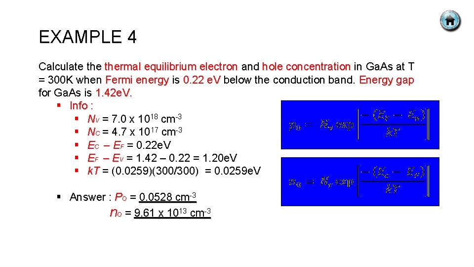
EXAMPLE 4 Calculate thermal equilibrium electron and hole concentration in Ga. As at T = 300 K when Fermi energy is 0. 22 e. V below the conduction band. Energy gap for Ga. As is 1. 42 e. V. § Info : § NV = 7. 0 x 1018 cm-3 § NC = 4. 7 x 1017 cm-3 § EC – EF = 0. 22 e. V § EF – EV = 1. 42 – 0. 22 = 1. 20 e. V § k. T = (0. 0259)(300/300) = 0. 0259 e. V § Answer : PO = 0. 0528 cm-3 n. O = 9. 61 x 1013 cm-3
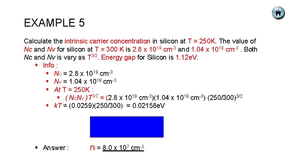
EXAMPLE 5 Calculate the intrinsic carrier concentration in silicon at T = 250 K. The value of Nc and Nv for silicon at T = 300 K is 2. 8 x 1019 cm-3 and 1. 04 x 1019 cm-3. Both Nc and Nv is vary as T 3/2. Energy gap for Silicon is 1. 12 e. V. § Info : § NC = 2. 8 x 1019 cm-3 § NV = 1. 04 x 1019 cm-3 § At T = 250 K : § ( NCNV )T 3/2 = (2. 8 x 1019 cm-3)(1. 04 x 1019 cm-3) (250/300)3/2 § k. T = (0. 0259)(250/300) = 0. 02158 e. V § Answer : ni = 8. 0 x 107 cm-3

TAKE A SIT & RELAX § Please watch this video and DON’T SLEEP! VIDEO 1
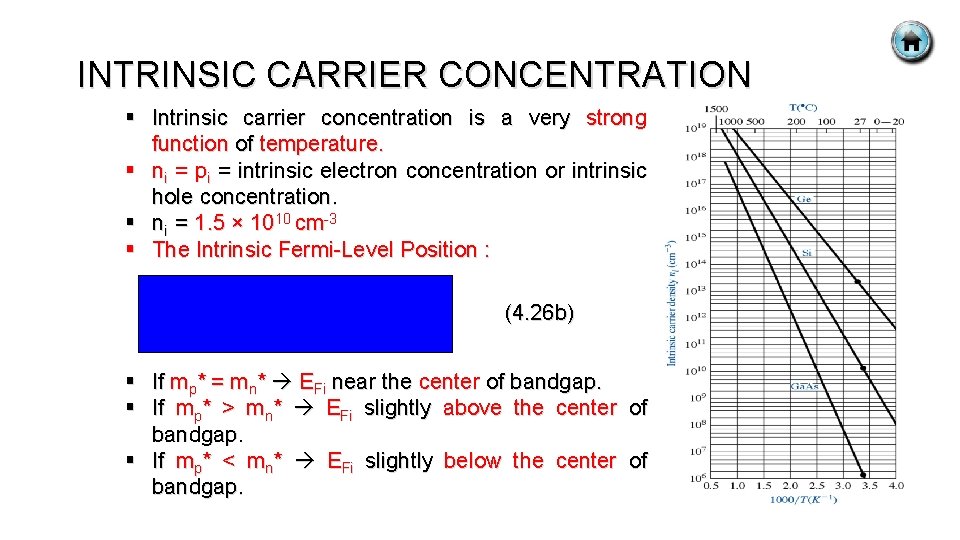
INTRINSIC CARRIER CONCENTRATION § Intrinsic carrier concentration is a very strong function of temperature. § ni = pi = intrinsic electron concentration or intrinsic hole concentration. § ni = 1. 5 × 1010 cm-3 § The Intrinsic Fermi-Level Position : (4. 26 b) § If mp* = mn* EFi near the center of bandgap. § If mp* > mn* EFi slightly above the center of bandgap. § If mp* < mn* EFi slightly below the center of bandgap.
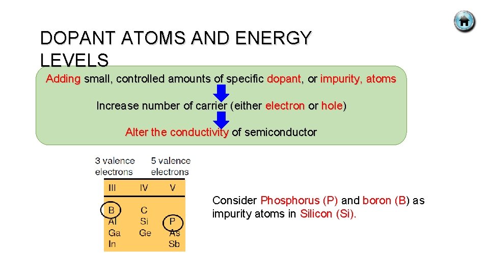
DOPANT ATOMS AND ENERGY LEVELS Adding small, controlled amounts of specific dopant, or impurity, atoms Increase number of carrier (either electron or hole) Alter the conductivity of semiconductor Consider Phosphorus (P) and boron (B) as impurity atoms in Silicon (Si).
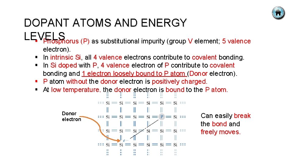
DOPANT ATOMS AND ENERGY LEVELS § Phosphorus (P) as substitutional impurity (group V element; 5 valence § § electron). In intrinsic Si, all 4 valence electrons contribute to covalent bonding. In Si doped with P, 4 valence electron of P contribute to covalent bonding and 1 electron loosely bound to P atom (Donor electron). P atom without the donor electron is positively charged. At low temperature, the donor electron is bound to the P atom. Donor electron Can easily break the bond and freely moves.
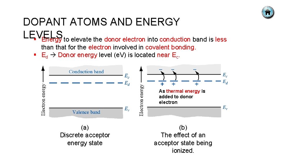
DOPANT ATOMS AND ENERGY LEVELS § Energy to elevate the donor electron into conduction band is less than that for the electron involved in covalent bonding. § Ed Donor energy level (e. V) is located near Ec. As thermal energy is added to donor electron (a) Discrete acceptor energy state (b) The effect of an acceptor state being ionized.
DOPANT ATOMS AND ENERGY LEVELS § When small energy is added, donor electron is elevated to § § § conduction band, leaving behind positively charged P ion. P atoms donate electron to conduction band P; donor impurity atom. Number of electron > number of hole n-type semiconductor (majority carrier is electron). The electron in the conduction band can move through the crystal generating current, while positively charged ion is fixed in the crystal. The donor impurity adds electrons to conduction band without creating holes in valence band. This material n-type (n for negatively charged electron).
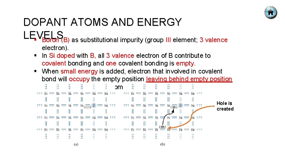
DOPANT ATOMS AND ENERGY LEVELS § Boron (B) as substitutional impurity (group III element; 3 valence electron). § In Si doped with B, all 3 valence electron of B contribute to covalent bonding and one covalent bonding is empty. § When small energy is added, electron that involved in covalent bond will occupy the empty position leaving behind empty position that associated with Si atom. Hole is created
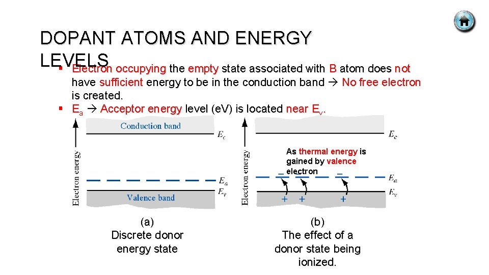
DOPANT ATOMS AND ENERGY LEVELS § Electron occupying the empty state associated with B atom does not have sufficient energy to be in the conduction band No free electron is created. § Ea Acceptor energy level (e. V) is located near Ev. As thermal energy is gained by valence electron (a) Discrete donor energy state (b) The effect of a donor state being ionized.
DOPANT ATOMS AND ENERGY LEVELS § When electron from valence band elevate to Ea, hole and negatively § § § charged B are created. B accepts electron from valence band B; acceptor impurity atom. No. of hole > no. of electron p-type material (majority carrier is hole). The hole can move through the crystal generating current, while negatively charged boron atom is fixed in the crystal. The acceptor atom generates holes in valence band without generating electrons in conduction band. This material p-type (p for positively charged hole).

EXTRINSIC SEMICONDUCTOR § Intrinsic semiconductor - Pure single-crystal semiconductor. § Extrinsic semiconductor - Semiconductor with dopant atoms. § Ionization energy : § The energy that required to elevate donor electron into the conduction (in case of donor impurity atom) or to elevate valence electron into acceptor state (in case of acceptor impurity atom).
EXTRINSIC SEMICONDUCTOR § Dopant atoms : § Group II (beryllium, zinc and cadmium) replacing Ga; acceptor. § Group VI (selenium, tellurium) replacing As; donor. § Group IV (Si and germanium) replacing Ga; donor and As; acceptor.
EXTRINSIC SEMICONDUCTOR § Extrinsic semiconductor is a semiconductor with controlled amounts of specific dopant or impurity atoms so that thermal equilibrium and hole concentrations are different from intrinsic carrier concentration. § One type of carrier predominates in extrinsic semiconductor. § Adding donor or acceptor impurity atoms changes : § Distribution of electron and holes. § Fermi energy. § Density of electrons in conduction band holes in valence band. § EF > EFi : The electron concentration is larger than hole concentration. § EF < EFi : The hole concentration is larger than electron concentration.
EXTRINSIC SEMICONDUCTOR § Since n 0 > p 0 : § The semiconductor n-type. § In n-type semiconductor, electrons as majority carrier and holes as minority carrier. § Since p 0 > n 0 : § The semiconductor p-type. § In p-type semiconductor, holes as majority carrier and electrons as minority carrier.
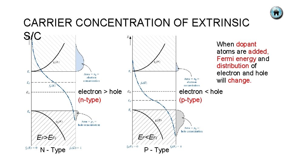
CARRIER CONCENTRATION OF EXTRINSIC S/C When dopant atoms are added, Fermi energy and distribution of electron and hole will change. electron > hole (n-type) EF>EFi N - Type electron < hole (p-type) EF<EFi P - Type
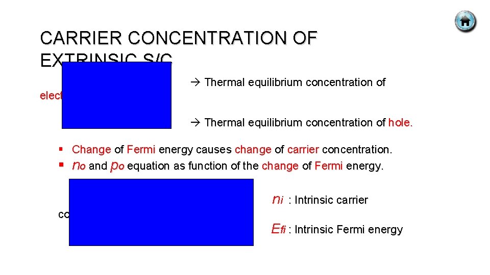
CARRIER CONCENTRATION OF EXTRINSIC S/C Thermal equilibrium concentration of electron. Thermal equilibrium concentration of hole. § Change of Fermi energy causes change of carrier concentration. § no and po equation as function of the change of Fermi energy. ni : Intrinsic carrier concentration Efi : Intrinsic Fermi energy
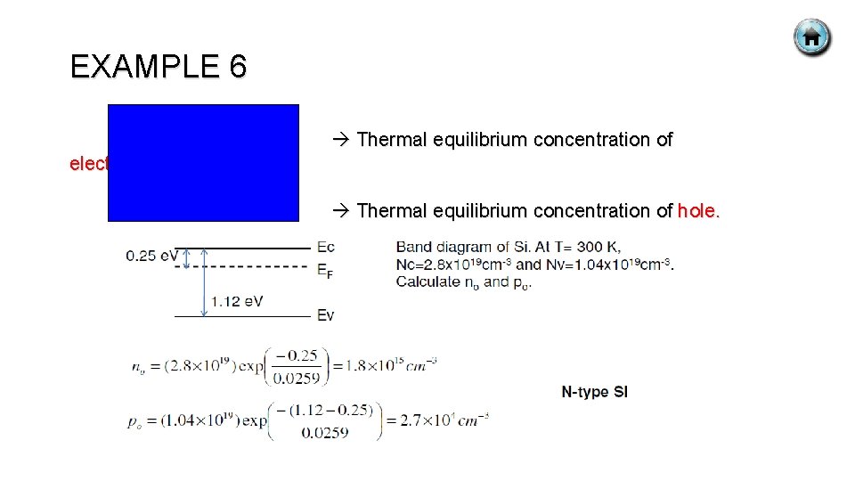
EXAMPLE 6 Thermal equilibrium concentration of electron. Thermal equilibrium concentration of hole.
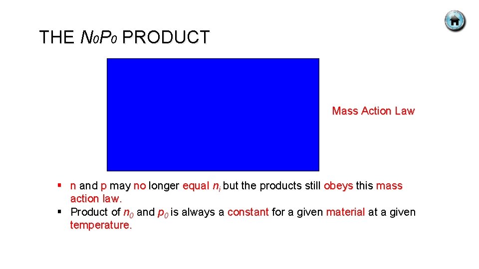
THE N 0 P 0 PRODUCT Mass Action Law § n and p may no longer equal ni but the products still obeys this mass action law. § Product of n 0 and p 0 is always a constant for a given material at a given temperature.
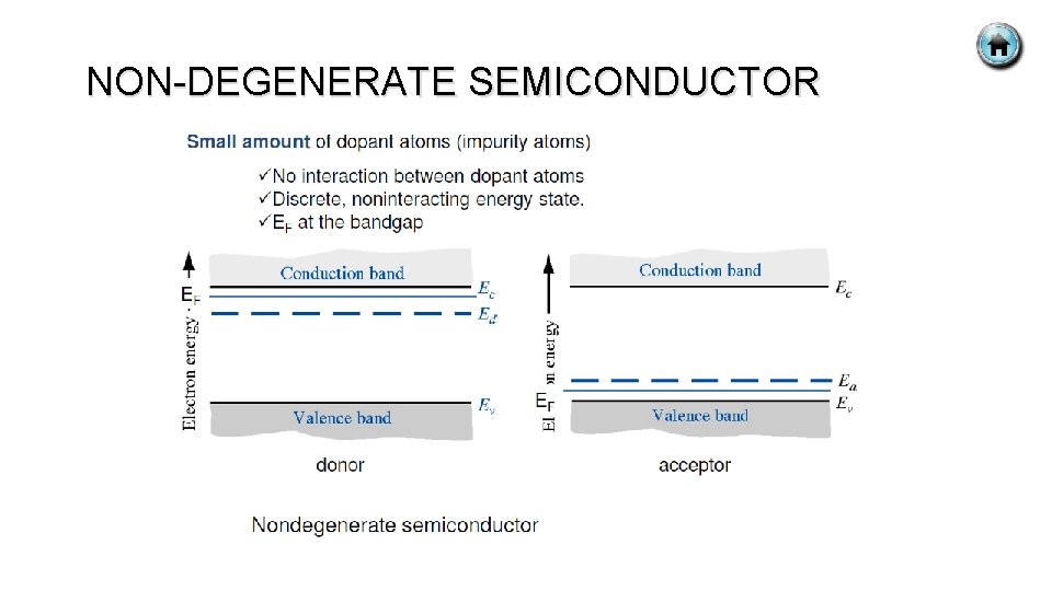
NON-DEGENERATE SEMICONDUCTOR
NON-DEGENERATE SEMICONDUCTOR § When dopant is added, we assumed that the concentration of dopant atoms added is small compared to density of host/semiconductor atoms. § The small number of impurity are spread far enough that no interaction between donor electrons e. g. n-type material. § It is assumed impurities introduce discrete and non-interacting donor energy states in n-type semiconductor and discrete and non -interacting acceptor state in p-type semiconductor. § Referred to as non-degenerate semiconductor. § If the impurity concentration increases, the distances between impurity atoms decreases and a point be reached when donor electrons interact with each other.
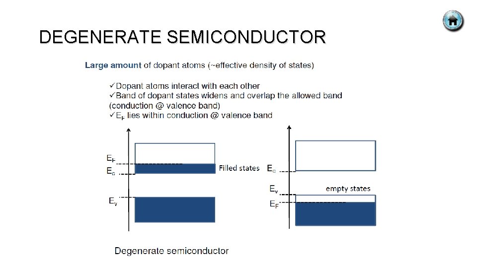
DEGENERATE SEMICONDUCTOR
DEGENERATE SEMICONDUCTOR § So the single discrete donor energy will split into band of energies. § And if the donor concentration further increases, the band of donor states widen and may overlap the bottom of conduction band. § It occurs when donor concentration becomes comparable with effective density of states. § The concentration of electrons in conduction band exceeds the density states Nc, the Fermi energy lies within conduction band. § Referred to as degenerate semiconductor.
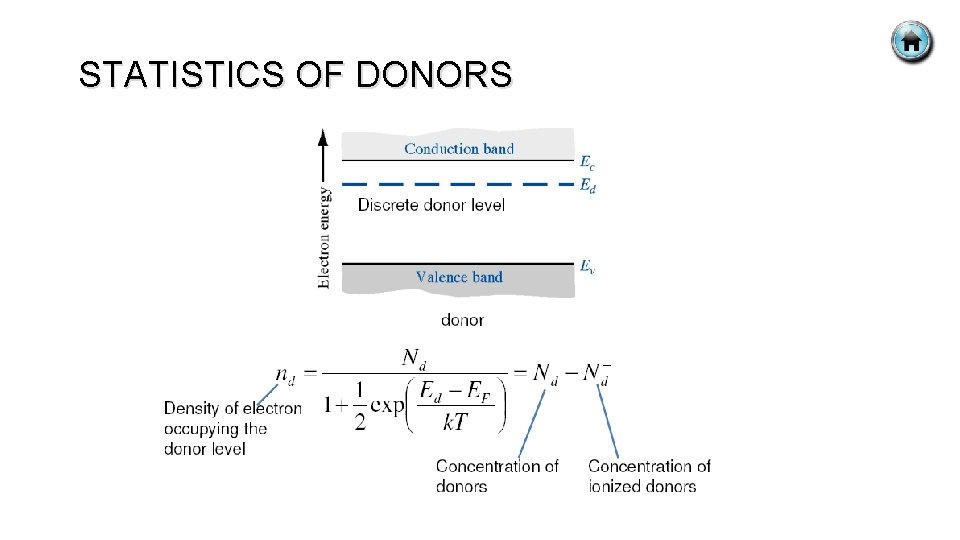
STATISTICS OF DONORS
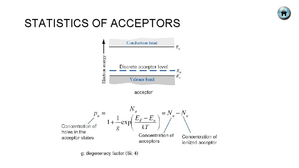
STATISTICS OF ACCEPTORS

TAKE A SIT & RELAX § Please watch this video and DON’T SLEEP! VIDEO 2
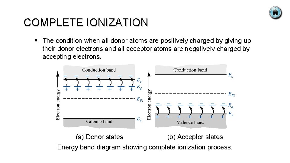
COMPLETE IONIZATION § The condition when all donor atoms are positively charged by giving up their donor electrons and all acceptor atoms are negatively charged by accepting electrons. (a) Donor states (b) Acceptor states Energy band diagram showing complete ionization process.
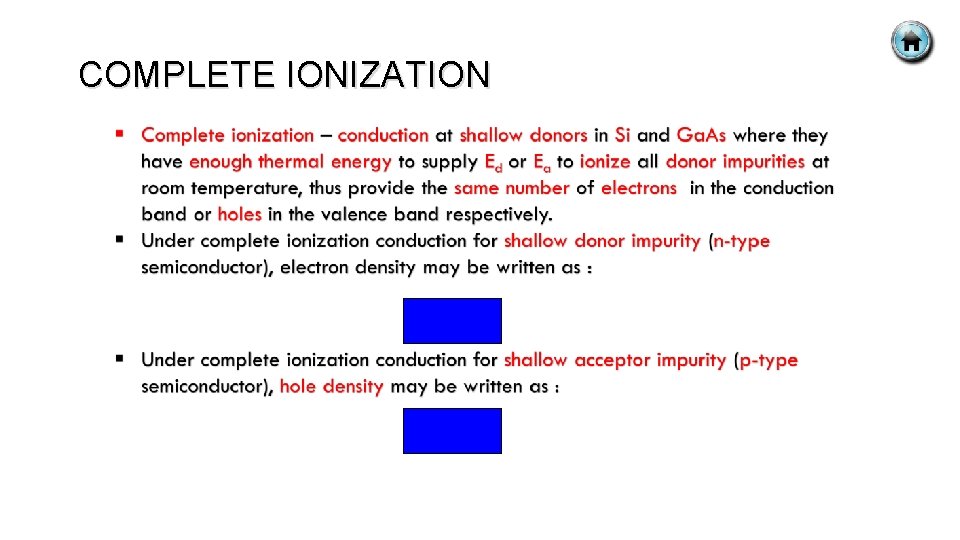
COMPLETE IONIZATION
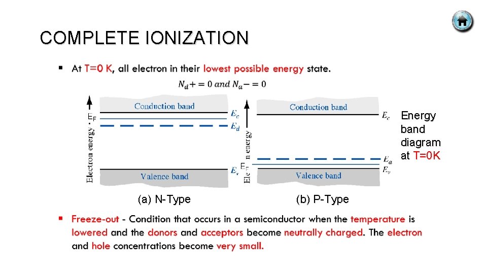
COMPLETE IONIZATION Energy band diagram at T=0 K (a) N-Type (b) P-Type
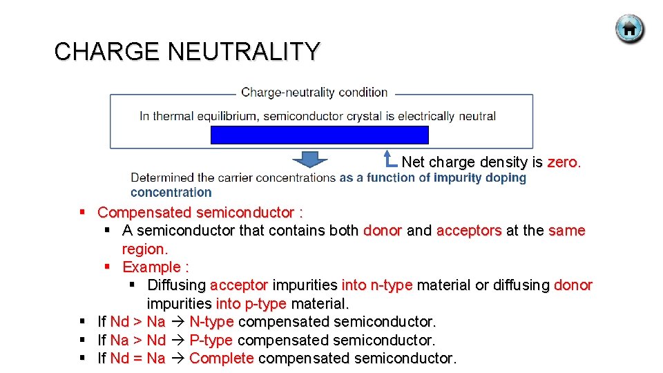
CHARGE NEUTRALITY Net charge density is zero. § Compensated semiconductor : § A semiconductor that contains both donor and acceptors at the same region. § Example : § Diffusing acceptor impurities into n-type material or diffusing donor impurities into p-type material. § If Nd > Na N-type compensated semiconductor. § If Na > Nd P-type compensated semiconductor. § If Nd = Na Complete compensated semiconductor.
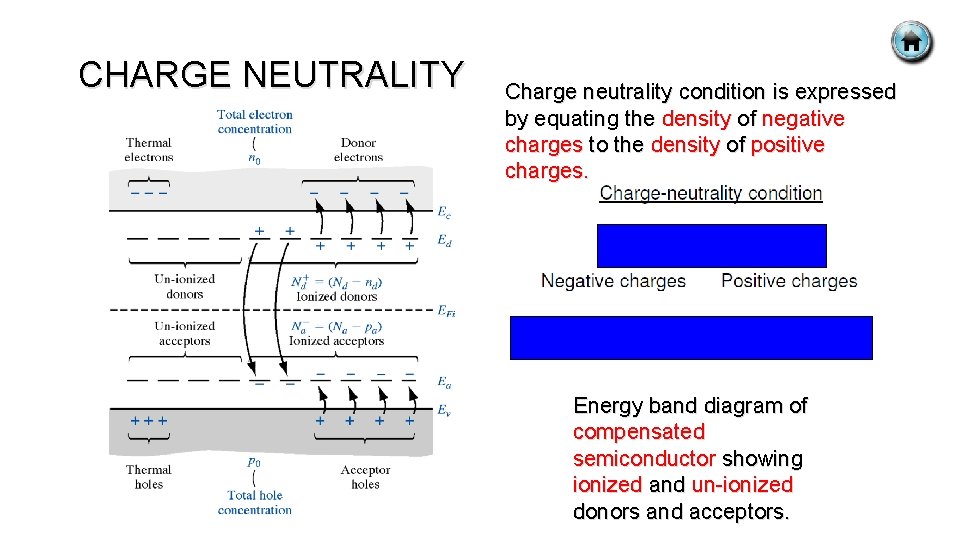
CHARGE NEUTRALITY Charge neutrality condition is expressed by equating the density of negative charges to the density of positive charges. Energy band diagram of compensated semiconductor showing ionized and un-ionized donors and acceptors.
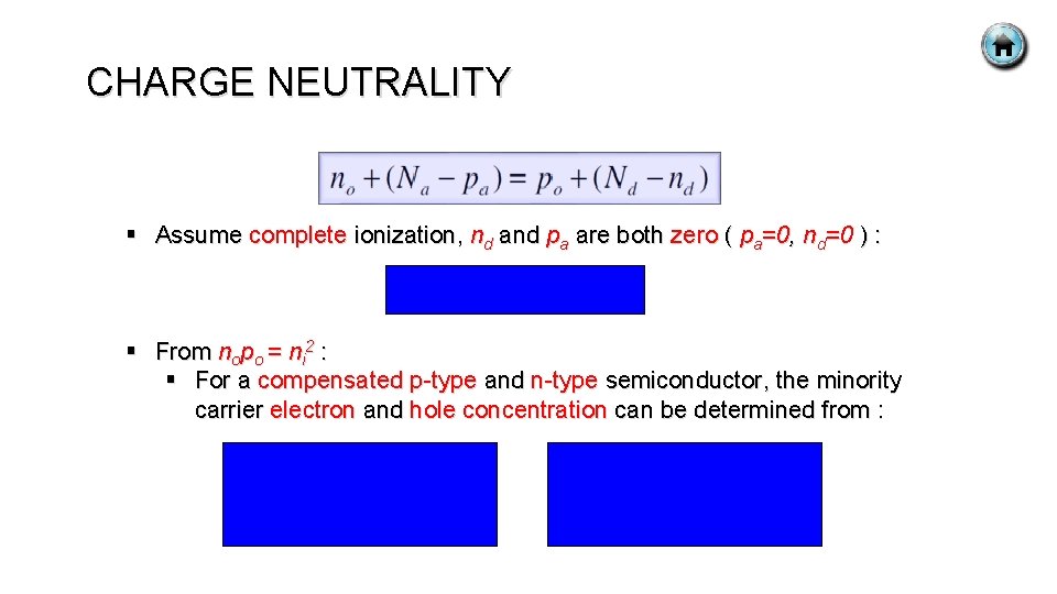
CHARGE NEUTRALITY § Assume complete ionization, nd and pa are both zero ( pa=0, nd=0 ) : § From nopo = ni 2 : § For a compensated p-type and n-type semiconductor, the minority carrier electron and hole concentration can be determined from :
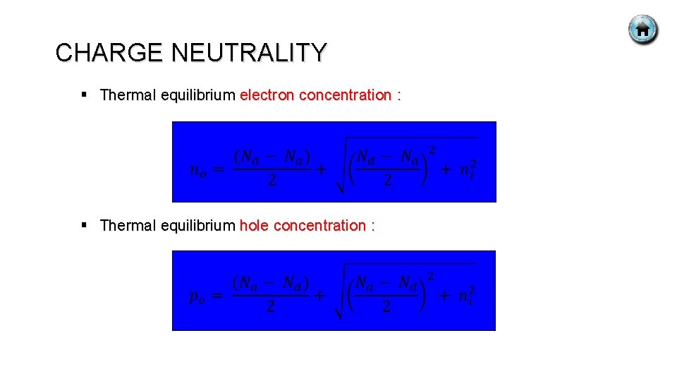
CHARGE NEUTRALITY § Thermal equilibrium electron concentration : § Thermal equilibrium hole concentration :
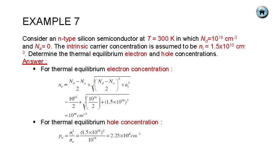
EXAMPLE 7 Consider an n-type silicon semiconductor at T = 300 K in which Nd=1016 cm-3 and Na= 0. The intrinsic carrier concentration is assumed to be ni = 1. 5 x 1010 cm 3. Determine thermal equilibrium electron and hole concentrations. Answer : § For thermal equilibrium electron concentration : § For thermal equilibrium hole concentration :
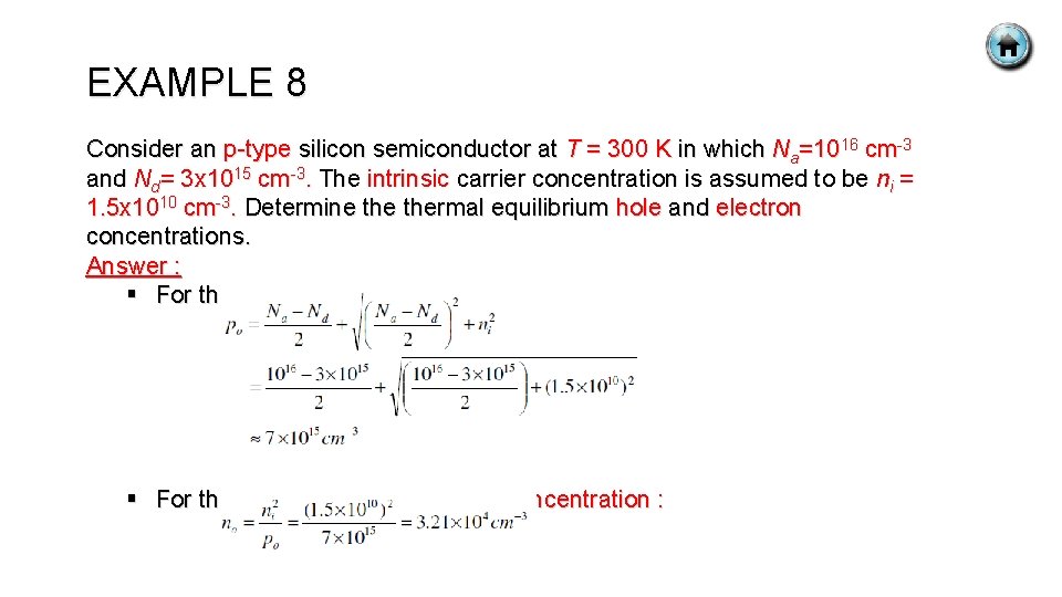
EXAMPLE 8 Consider an p-type silicon semiconductor at T = 300 K in which Na=1016 cm-3 and Nd= 3 x 1015 cm-3. The intrinsic carrier concentration is assumed to be ni = 1. 5 x 1010 cm-3. Determine thermal equilibrium hole and electron concentrations. Answer : § For thermal equilibrium hole concentration : § For thermal equilibrium electron concentration :
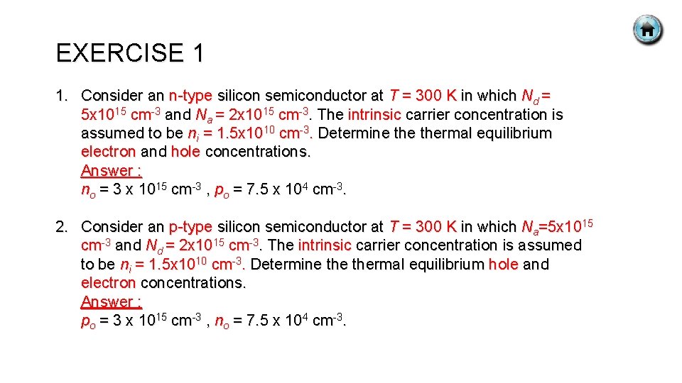
EXERCISE 1 1. Consider an n-type silicon semiconductor at T = 300 K in which Nd = 5 x 1015 cm-3 and Na = 2 x 1015 cm-3. The intrinsic carrier concentration is assumed to be ni = 1. 5 x 1010 cm-3. Determine thermal equilibrium electron and hole concentrations. Answer : no = 3 x 1015 cm-3 , po = 7. 5 x 104 cm-3. 2. Consider an p-type silicon semiconductor at T = 300 K in which Na=5 x 1015 cm-3 and Nd = 2 x 1015 cm-3. The intrinsic carrier concentration is assumed to be ni = 1. 5 x 1010 cm-3. Determine thermal equilibrium hole and electron concentrations. Answer : po = 3 x 1015 cm-3 , no = 7. 5 x 104 cm-3.
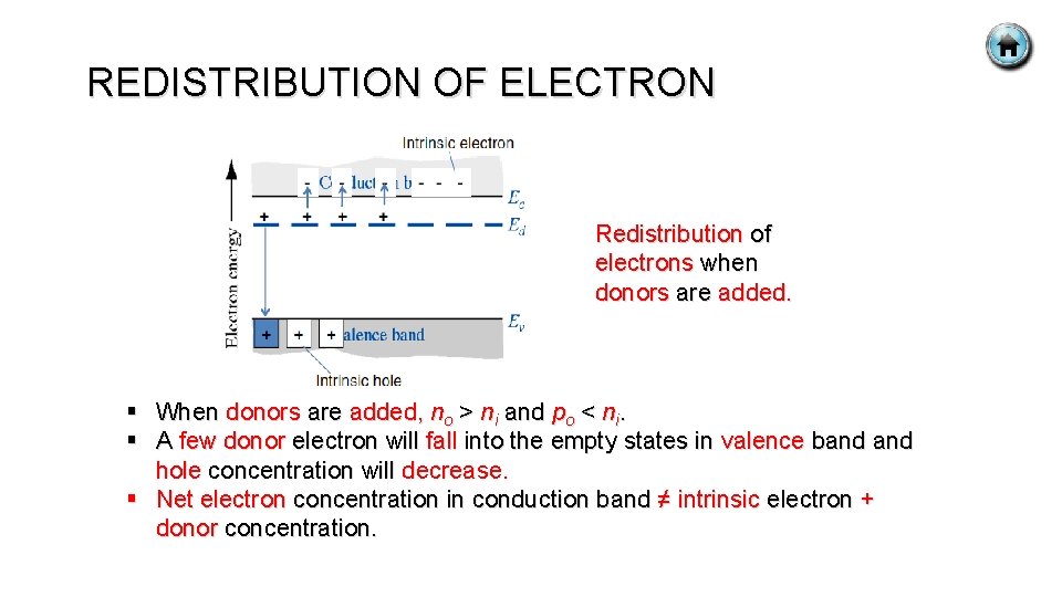
REDISTRIBUTION OF ELECTRON Redistribution of electrons when donors are added. § When donors are added, no > ni and po < ni. § A few donor electron will fall into the empty states in valence band hole concentration will decrease. § Net electron concentration in conduction band ≠ intrinsic electron + donor concentration.
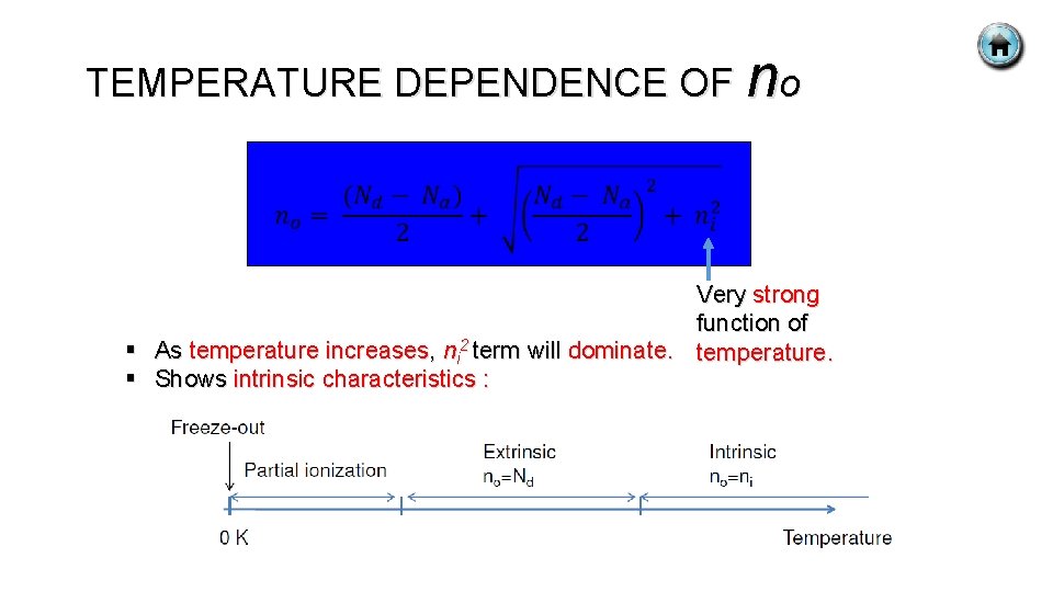
TEMPERATURE DEPENDENCE OF no Very strong function of § As temperature increases, ni 2 term will dominate. temperature. § Shows intrinsic characteristics :

POSITION OF FERMI ENERGY LEVEL § As a function of doping concentration and temperature. § Equations for position of Fermi level (N-type) : Notes : § For compensated semiconductor, no = Nd - Na : § For intrinsic semiconductor (N-type) :

POSITION OF FERMI ENERGY LEVEL § As a function of doping concentration and temperature. § Equations for position of Fermi level (P-type) : Notes : § For compensated semiconductor, po = Na - Nd : § For intrinsic semiconductor (P-type) : Video 3
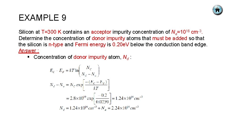
EXAMPLE 9 Silicon at T=300 K contains an acceptor impurity concentration of Na=1016 cm-3. Determine the concentration of donor impurity atoms that must be added so that the silicon is n-type and Fermi energy is 0. 20 e. V below the conduction band edge. Answer : § Concentration of donor impurity atom, Nd :
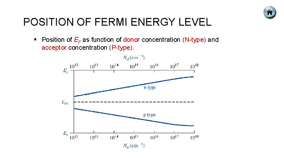
POSITION OF FERMI ENERGY LEVEL § Position of EF as function of donor concentration (N-type) and acceptor concentration (P-type).
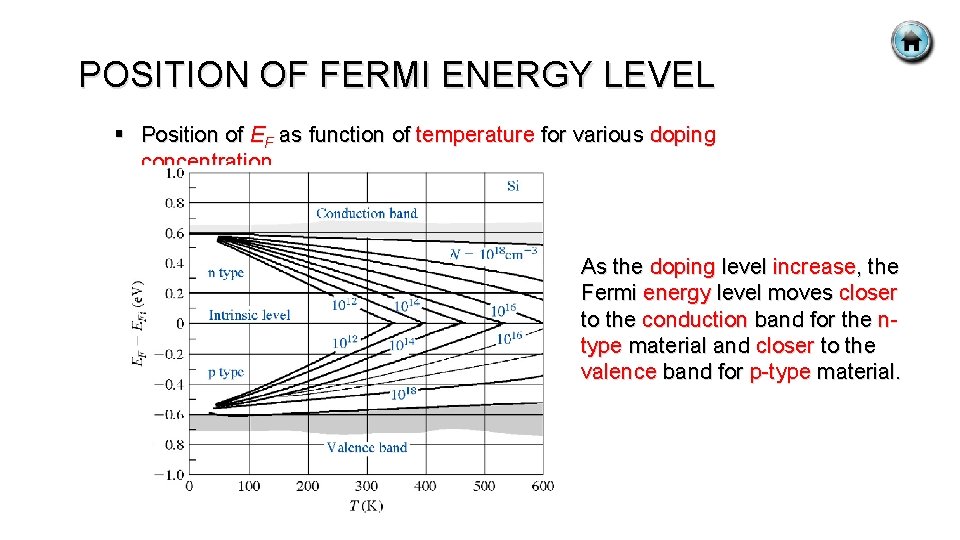
POSITION OF FERMI ENERGY LEVEL § Position of EF as function of temperature for various doping concentration. As the doping level increase, the Fermi energy level moves closer to the conduction band for the ntype material and closer to the valence band for p-type material.
CHECK AND BALANCE § Ability to describe and differentiate the following idea for extrinsic and intrinsic semiconductor : Energy band diagram. Density of states (DOS). Carrier distribution. Acceptor and donor energy level. Electron and holes terminology. Fermi level position.
IMPORTANT TERMS § Equilibrium : § No external forces such as voltages, electric fields, magnetic fields or temperature gradients are acting on the semiconductor. § Carrier : § Particles that can freely move and contribute to the current flow (conduction). § Intrinsic semiconductor : § Pure crystal. § Extrinsic semiconductor : § Addition of specific impurity atom to the crystal where the dominant charge carrier in semiconductor can either be electrons in conduction band or holes in valence band.
IMPORTANT TERMS § Acceptor atoms : § Impurity atoms added to a semiconductor to create a p-type material. § Donor atoms : § Impurity atoms added to a semiconductor to create n-type material. § Complete ionization : § The condition when all donor atoms are positively charged by giving up their donor electrons and all acceptor atoms are negatively charged by accepting electrons. § Freeze-out : § The condition that occurs in a semiconductor when the temperature is lowered and the donors and acceptors become neutrally charged. The electron and hole concentrations become very small.

NEXT WEEK CHAPTER 4 : Carrier Transport Phenomena. § Duration : 2 Weeks ( W 5 -W 6 ). § Tutorial 2 : Week 6.
- Slides: 75