Chapter 3 Special Purpose Diodes ELECTRONICs 1 PLT

- Slides: 51

Chapter 3 Special. Purpose Diodes ELECTRONICs 1 PLT 107 ELEKTRONIK 1

Objectives Ø Describe the characteristic of zener diode and analyze its operation. Ø Explain how a zener is used in voltage regulation and limiting Ø Describe the varactor diode and it’s variable capacitance characteristics Ø Discuss the operation and characteristics of LEDs and photodiodes Ø Discuss the basic characteristics of the current regulator diode, the pin diode, the step-recovery diode, the tunnel diode, and the laser diode.

Lecture’s content Zener diodes Zener diode applications Varactor diodes Optical diodes Troubleshooting Summary

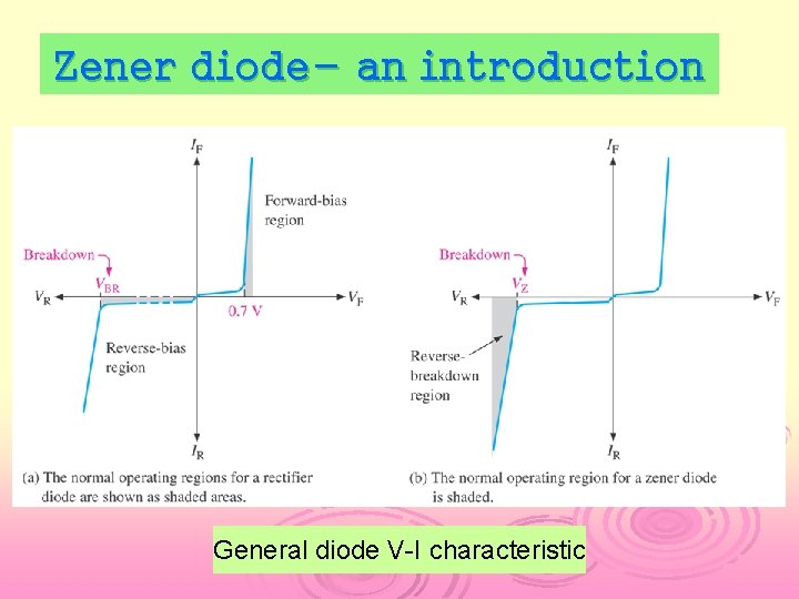
Zener diode – an introduction Zener diode – silicon pn-junction device that is designed for operation in the reverse-biased region. Ø The basic function of zener diode is to maintain a nearly constant dc voltage under properating condition. Ø Typically it is used to provide a stable reference voltage for use in power supplies, voltmeter and other equipment. Ø Zener diode symbol

Zener diode-an introduction Ø Breakdown voltage – set by controlling the doping level during manufacture. Ø When diode reached reverse breakdown – voltage remains constant even though current change drastically. Ø If zener diode is FB – operates the same as a rectifier diode. Ø A zener diode is much like a normal diode – but it is placed in the circuit in reverse bias and operates in reverse breakdown. Ø Note that it’s forward characteristics are just like a normal diode.

Zener diode- an introduction General diode V-I characteristic

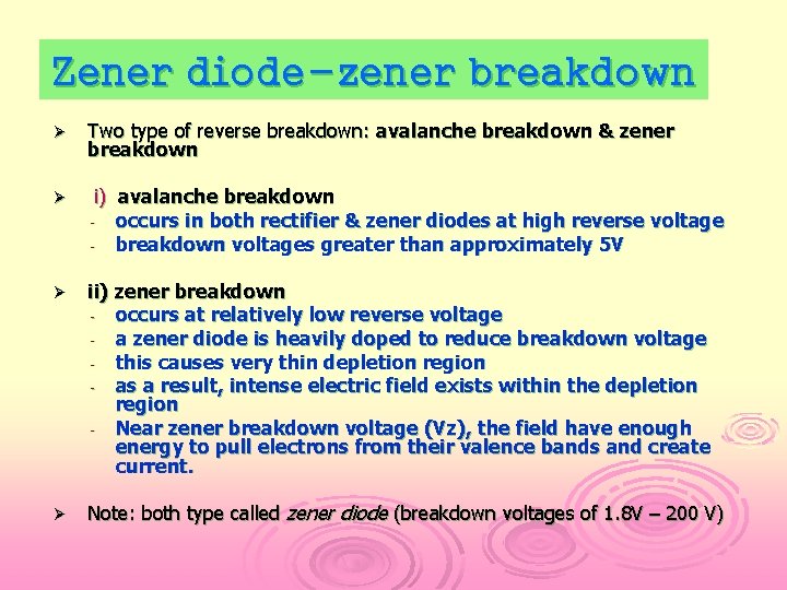
Zener diode-zener breakdown Ø Two type of reverse breakdown: avalanche breakdown & zener breakdown Ø i) avalanche breakdown occurs in both rectifier & zener diodes at high reverse voltage breakdown voltages greater than approximately 5 V Ø ii) zener breakdown occurs at relatively low reverse voltage a zener diode is heavily doped to reduce breakdown voltage this causes very thin depletion region as a result, intense electric field exists within the depletion region Near zener breakdown voltage (Vz), the field have enough energy to pull electrons from their valence bands and create current. Ø Note: both type called zener diode (breakdown voltages of 1. 8 V – 200 V)

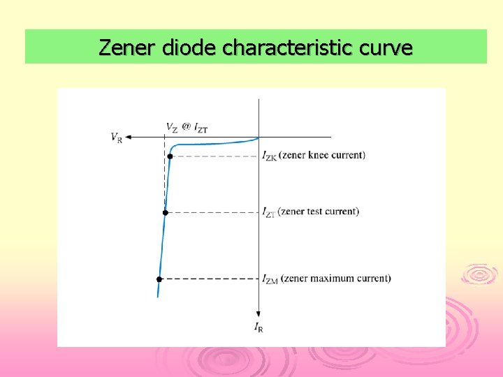
Zener diode characteristic curve

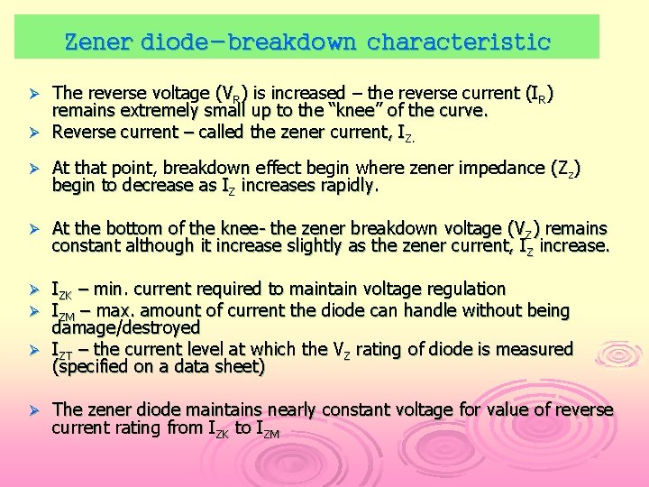
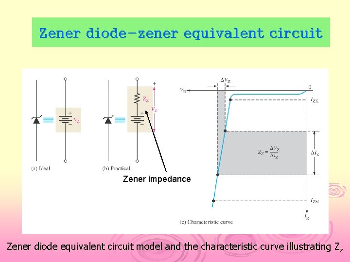
Zener diode-breakdown characteristic The reverse voltage (VR) is increased – the reverse current (IR) remains extremely small up to the “knee” of the curve. Ø Reverse current – called the zener current, IZ. Ø Ø At that point, breakdown effect begin where zener impedance (Z z) begin to decrease as IZ increases rapidly. Ø At the bottom of the knee- the zener breakdown voltage (V Z) remains constant although it increase slightly as the zener current, I Z increase. IZK – min. current required to maintain voltage regulation IZM – max. amount of current the diode can handle without being damage/destroyed Ø IZT – the current level at which the VZ rating of diode is measured (specified on a data sheet) Ø Ø Ø The zener diode maintains nearly constant voltage for value of reverse current rating from IZK to IZM

Zener diode-zener equivalent circuit Zener impedance Zener diode equivalent circuit model and the characteristic curve illustrating Z z

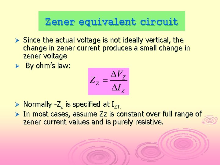
Zener equivalent circuit Since the actual voltage is not ideally vertical, the change in zener current produces a small change in zener voltage Ø By ohm’s law: Ø Normally -Zz is specified at IZT. Ø In most cases, assume Zz is constant over full range of zener current values and is purely resistive. Ø

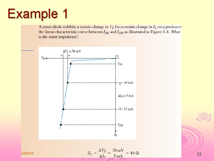
Example 1 12

Question 1 Calculate the zener impedance if the change in zener voltage is 100 m. V for a 20 m. A change in zener current on the linear portion of the characteristic curve. 13

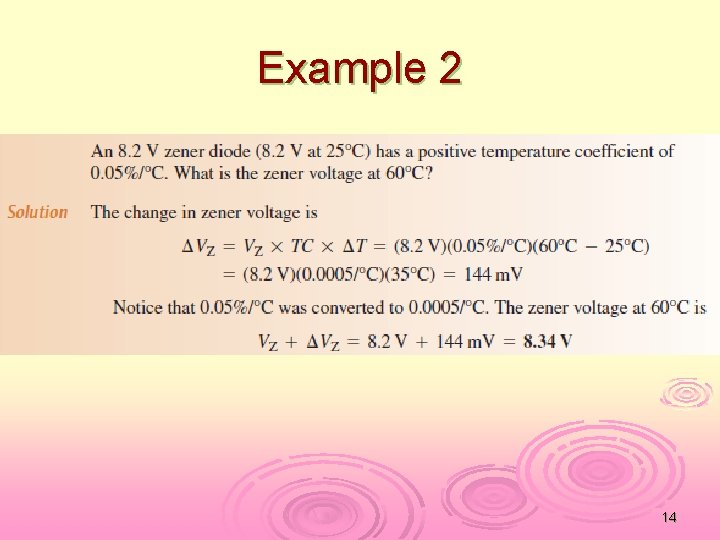
Example 2 14

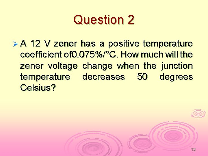
Question 2 ØA 12 V zener has a positive temperature coefficient of 0. 075%/°C. How much will the zener voltage change when the junction temperature decreases 50 degrees Celsius? 15

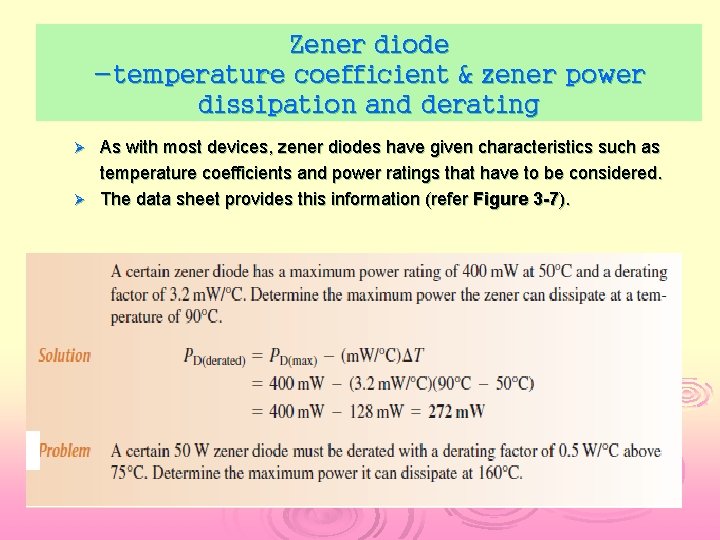
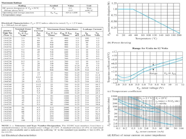
Zener diode -temperature coefficient & zener power dissipation and derating As with most devices, zener diodes have given characteristics such as temperature coefficients and power ratings that have to be considered. Ø The data sheet provides this information (refer Figure 3 -7). Ø


Zener diode applications -an introduction Ø Zener Ø Ø diode can be used as: Voltage regulator to provide stable reference voltage. Simple limiter or clipper

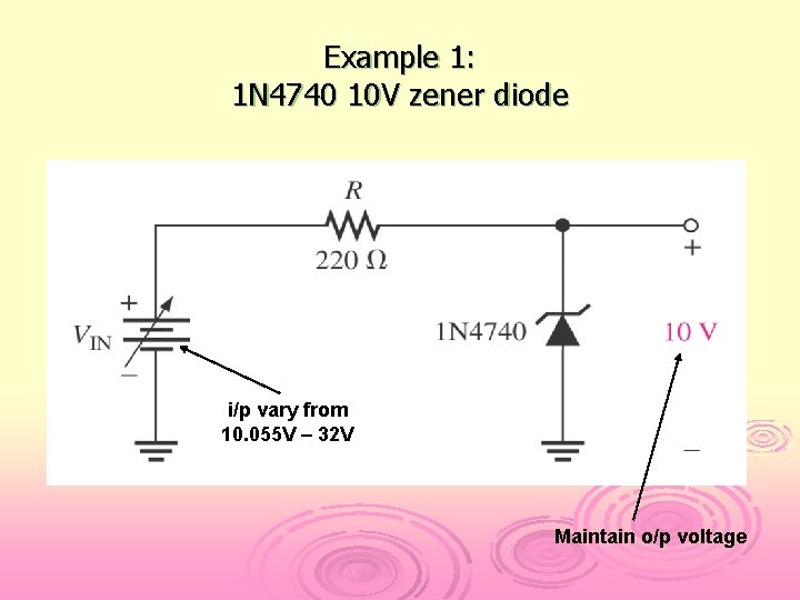
Example 1: 1 N 4740 10 V zener diode i/p vary from 10. 055 V – 32 V Maintain o/p voltage

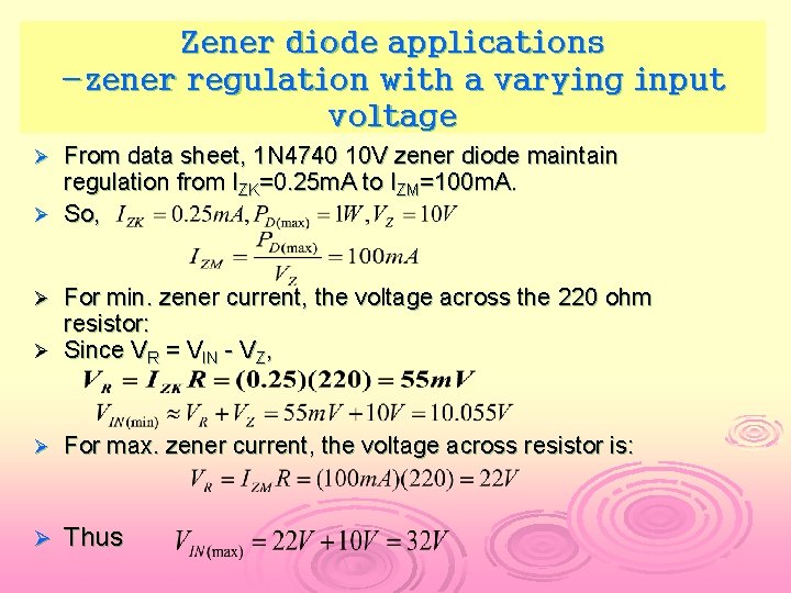
Zener diode applications -zener regulation with a varying input voltage From data sheet, 1 N 4740 10 V zener diode maintain regulation from IZK=0. 25 m. A to IZM=100 m. A. Ø So, Ø For min. zener current, the voltage across the 220 ohm resistor: Ø Since VR = VIN - VZ, Ø Ø For max. zener current, the voltage across resistor is: Ø Thus

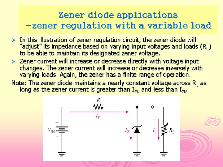
Zener diode applications -zener regulation with a variable load In this illustration of zener regulation circuit, the zener diode will “adjust” its impedance based on varying input voltages and loads (R L) to be able to maintain its designated zener voltage. Ø Zener current will increase or decrease directly with voltage input changes. The zener current will increase or decrease inversely with varying loads. Again, the zener has a finite range of operation. Note: The zener diode maintains a nearly constant voltage across R L as long as the zener current is greater than IZK and less than IZM Ø

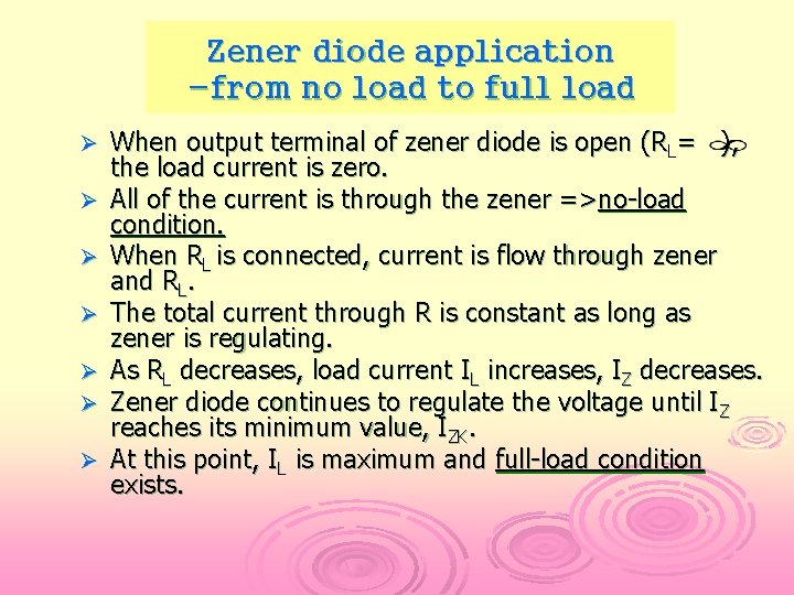
Zener diode application -from no load to full load Ø Ø Ø Ø When output terminal of zener diode is open (RL= ), the load current is zero. All of the current is through the zener =>no-load condition. When RL is connected, current is flow through zener and RL. The total current through R is constant as long as zener is regulating. As RL decreases, load current IL increases, IZ decreases. Zener diode continues to regulate the voltage until IZ reaches its minimum value, IZK. At this point, IL is maximum and full-load condition exists.

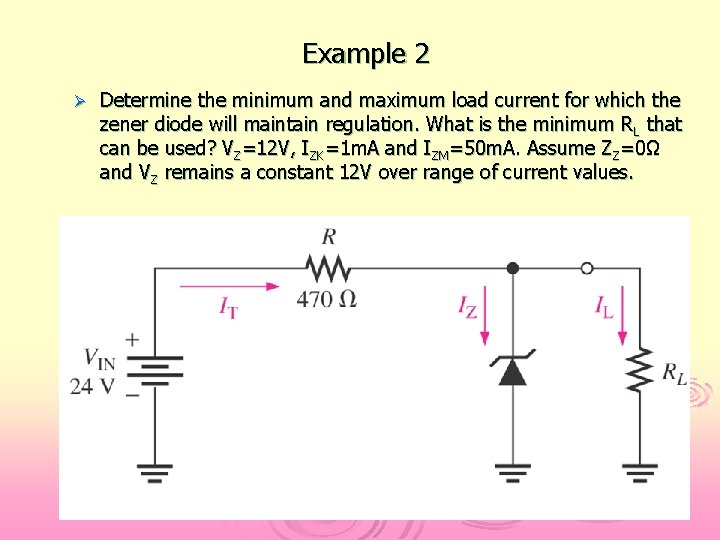
Example 2 Ø Determine the minimum and maximum load current for which the zener diode will maintain regulation. What is the minimum R L that can be used? VZ=12 V, IZK=1 m. A and IZM=50 m. A. Assume ZZ=0Ω and VZ remains a constant 12 V over range of current values.

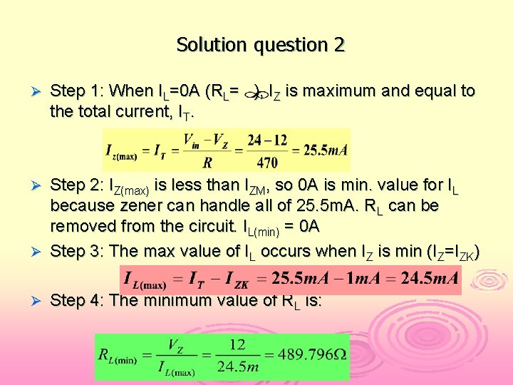
Solution question 2 Ø Step 1: When IL=0 A (RL= ), IZ is maximum and equal to the total current, IT. Step 2: IZ(max) is less than IZM, so 0 A is min. value for IL because zener can handle all of 25. 5 m. A. RL can be removed from the circuit. IL(min) = 0 A Ø Step 3: The max value of IL occurs when IZ is min (IZ=IZK) Ø Ø Step 4: The minimum value of RL is:

Question 3 Ø Zener Diode question Ø A 5. 0 V stabilised power supply is required to be produced from a 12 V DC power supply input source. The maximum power rating PZ of the zener diode is 2 W. Using the zener regulator circuit above calculate: 25

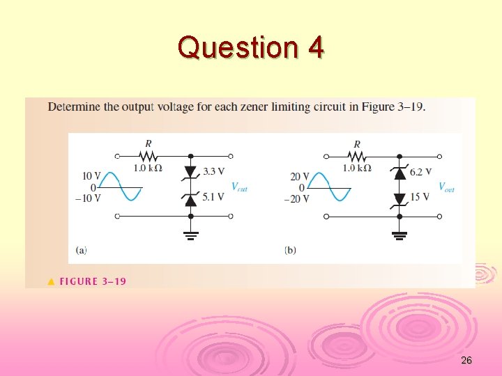
Question 4 26

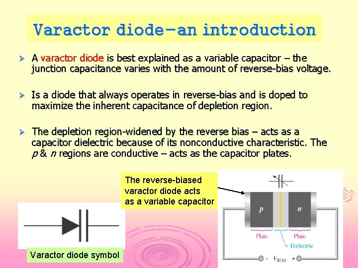
Varactor diode-an introduction Ø A varactor diode is best explained as a variable capacitor – the junction capacitance varies with the amount of reverse-bias voltage. Ø Is a diode that always operates in reverse-bias and is doped to maximize the inherent capacitance of depletion region. Ø The depletion region-widened by the reverse bias – acts as a capacitor dielectric because of its nonconductive characteristic. The p & n regions are conductive – acts as the capacitor plates. The reverse-biased varactor diode acts as a variable capacitor Varactor diode symbol

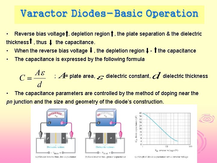
Varactor Diodes-Basic Operation • Reverse bias voltage , depletion region , the plate separation & the dielectric thickness , thus the capacitance. • When the reverse bias voltage • The capacitance is expressed by the following formula ; • , the depletion region = plate area, - dielectric constant, the capacitance dielectric thickness The capacitance parameters are controlled by the method of doping near the pn junction and the size and geometry of the diode’s construction.

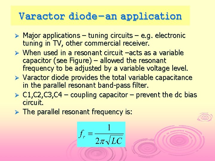
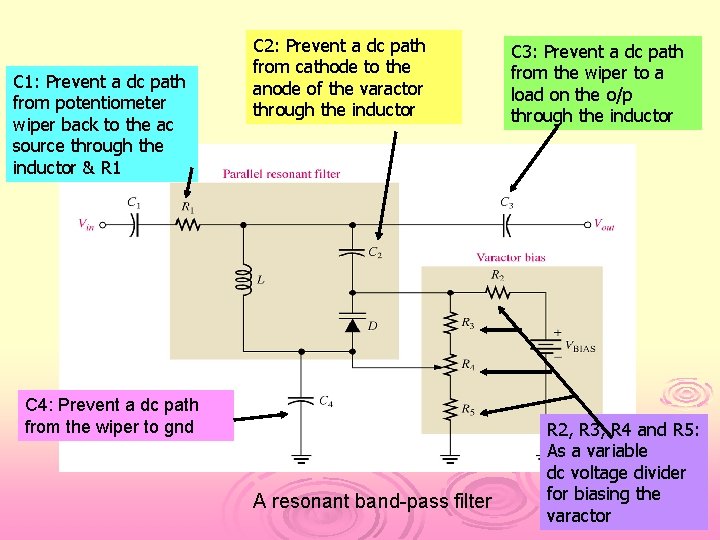
Varactor diode-an application Ø Ø Ø Major applications – tuning circuits – e. g. electronic tuning in TV, other commercial receiver. When used in a resonant circuit –acts as a variable capacitor (see Figure) – allowed the resonant frequency to be adjusted by a variable voltage level. Varactor diode provides the total variable capacitance in the parallel resonant band-pass filter. C 1, C 2, C 3, C 4 – coupling capacitor – prevent the dc bias circuit. The parallel resonant frequency is:

C 1: Prevent a dc path from potentiometer wiper back to the ac source through the inductor & R 1 C 2: Prevent a dc path from cathode to the anode of the varactor through the inductor C 4: Prevent a dc path from the wiper to gnd A resonant band-pass filter C 3: Prevent a dc path from the wiper to a load on the o/p through the inductor R 2, R 3, R 4 and R 5: As a variable dc voltage divider for biasing the varactor

Optical diode-an introduction Ø Two types of optoelectronic devices: v v The light-emitting diode (LED) – a light emitter Photodiode – a light detector

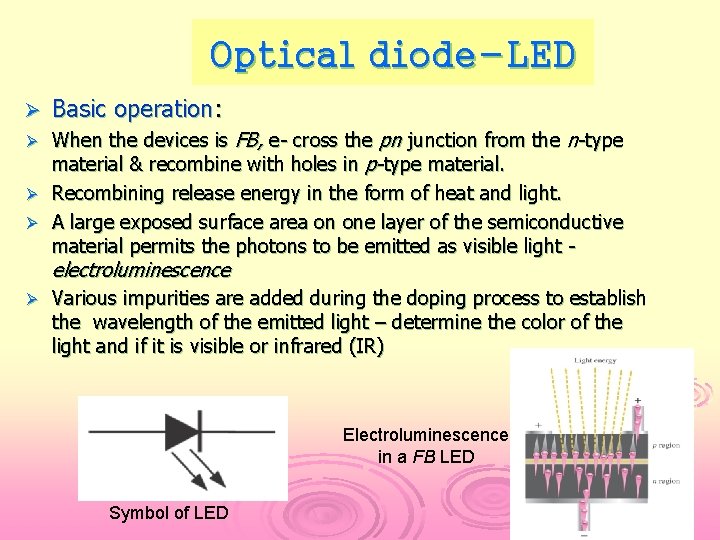
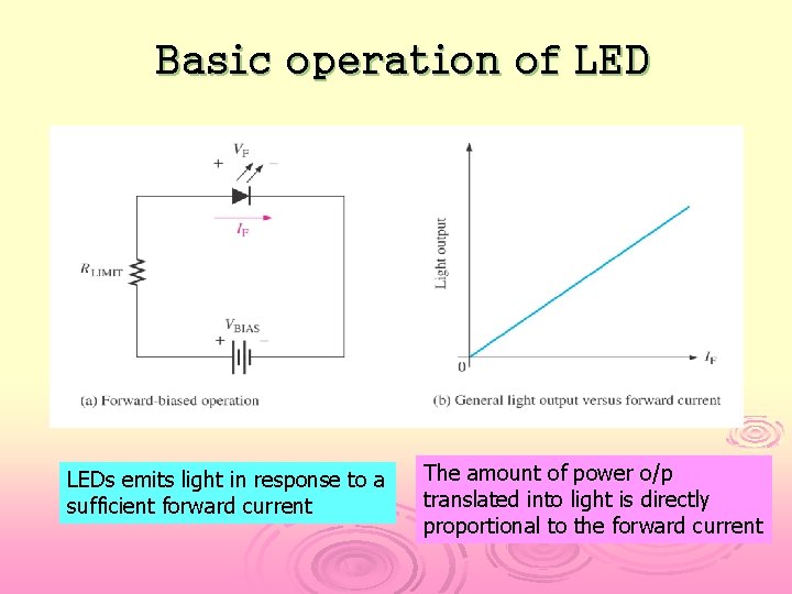
Optical diode-LED Ø Basic operation: When the devices is FB, e- cross the pn junction from the n-type material & recombine with holes in p-type material. Ø Recombining release energy in the form of heat and light. Ø A large exposed surface area on one layer of the semiconductive material permits the photons to be emitted as visible light Ø electroluminescence Ø Various impurities are added during the doping process to establish the wavelength of the emitted light – determine the color of the light and if it is visible or infrared (IR) Electroluminescence in a FB LED Symbol of LED

Optical diode-LED Ø LED Semiconductor Materials: l l l Ø Early LEDs - Ga. As 1 st visible red LEDs – gallium arsenide phosphide (Ga. As. P) on a Ga. As subtrate Ga. P substrate – brighter red LEDs & orange LEDs Ga. As LEDs – emit infrared (IR) readiation – invisible Others LEDs – refer textbook pg. 131. LED Biasing: l l l The forward voltage across an LED is considerably greater than for a silicon diode The max. VF for LEDs is 1. 2 V – 3. 2 V Reverse breakdown << for a silicon rectifier diode (typically 3 V – 10 V)

Basic operation of LEDs emits light in response to a sufficient forward current The amount of power o/p translated into light is directly proportional to the forward current

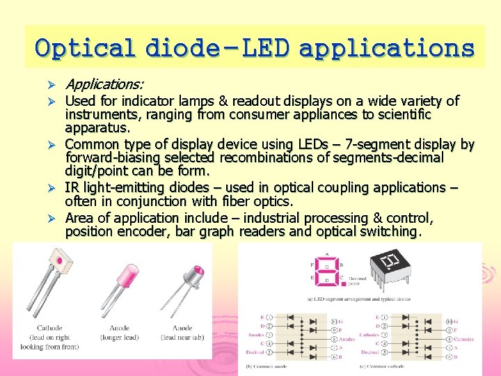
Optical diode-LED applications Ø Ø Ø Applications: Used for indicator lamps & readout displays on a wide variety of instruments, ranging from consumer appliances to scientific apparatus. Common type of display device using LEDs – 7 -segment display by forward-biasing selected recombinations of segments-decimal digit/point can be form. IR light-emitting diodes – used in optical coupling applications – often in conjunction with fiber optics. Area of application include – industrial processing & control, position encoder, bar graph readers and optical switching.

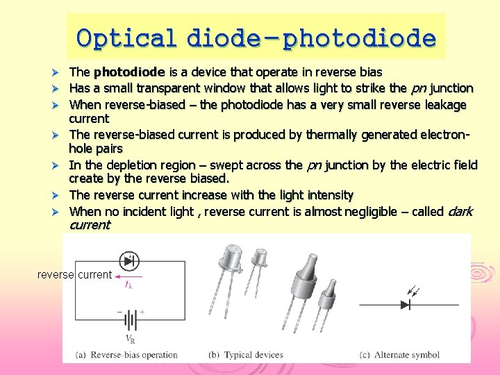
Optical diode-photodiode Ø Ø Ø Ø The photodiode is a device that operate in reverse bias Has a small transparent window that allows light to strike the pn junction When reverse-biased – the photodiode has a very small reverse leakage current The reverse-biased current is produced by thermally generated electronhole pairs In the depletion region – swept across the pn junction by the electric field create by the reverse biased. The reverse current increase with the light intensity When no incident light , reverse current is almost negligible – called dark current reverse current

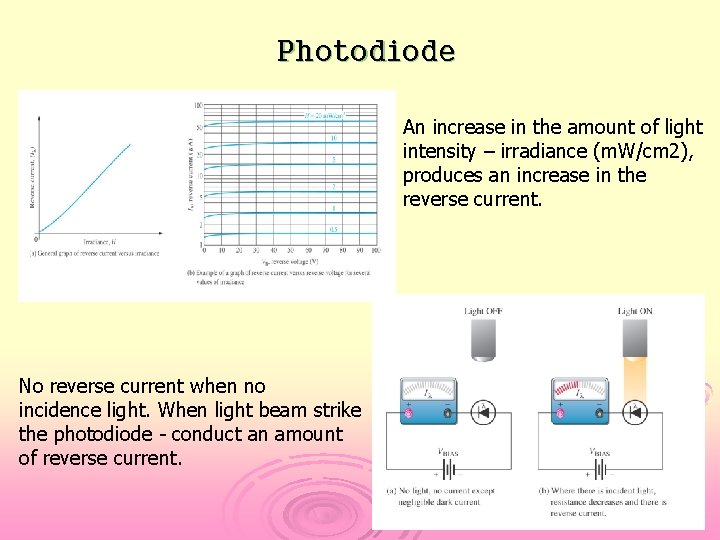
Photodiode An increase in the amount of light intensity – irradiance (m. W/cm 2), produces an increase in the reverse current. No reverse current when no incidence light. When light beam strike the photodiode - conduct an amount of reverse current.

Other types of diode v Current Regulator Diode v Schottky Diode v PIN Diode v Step-recovery Diode v Tunnel Diode v Laser Diode

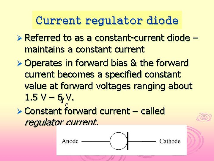
Current regulator diode Ø Referred to as a constant-current diode – maintains a constant current Ø Operates in forward bias & the forward current becomes a specified constant value at forward voltages ranging about 1. 5 V – 6 V. Ø Constant forward current – called regulator current,

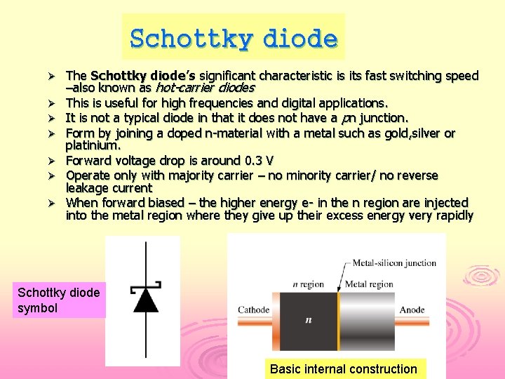
Schottky diode Ø Ø Ø Ø The Schottky diode’s significant characteristic is its fast switching speed –also known as hot-carrier diodes This is useful for high frequencies and digital applications. It is not a typical diode in that it does not have a pn junction. Form by joining a doped n-material with a metal such as gold, silver or platinium. Forward voltage drop is around 0. 3 V Operate only with majority carrier – no minority carrier/ no reverse leakage current When forward biased – the higher energy e- in the n region are injected into the metal region where they give up their excess energy very rapidly Schottky diode symbol Basic internal construction

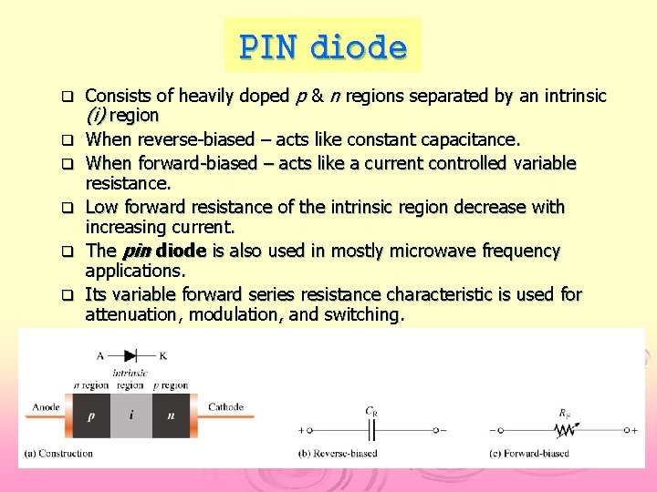
PIN diode q q q Consists of heavily doped p & n regions separated by an intrinsic (i) region When reverse-biased – acts like constant capacitance. When forward-biased – acts like a current controlled variable resistance. Low forward resistance of the intrinsic region decrease with increasing current. The pin diode is also used in mostly microwave frequency applications. Its variable forward series resistance characteristic is used for attenuation, modulation, and switching.

Step-recovery diode Ø The step-recovery diode is used in very high frequency (VHF) and also used for fast switching applications. Ø This is achieved by reduced doping at the junction.

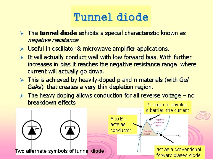
Tunnel diode Ø Ø Ø The tunnel diode exhibits a special characteristic known as negative resistance. Useful in oscillator & microwave amplifier applications. It will actually conduct well with low forward bias. With further increases in bias it reaches the negative resistance range where current will actually go down. This is achieved by heavily-doped p and n materials (with Ge/ Ga. As) that creates a very thin depletion region. The heavy doping allows conduction for all reverse voltage – no breakdown effects VF begin to develop a barrier- the current A to B – acts as conductor Two alternate symbols of tunnel diode act as a conventional forward biased diode

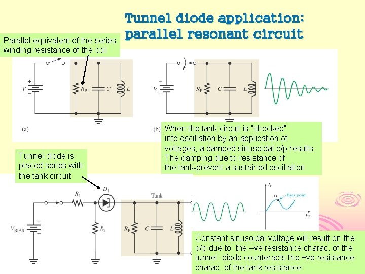
Parallel equivalent of the series winding resistance of the coil Tunnel diode is placed series with the tank circuit Tunnel diode application: parallel resonant circuit When the tank circuit is ”shocked” into oscillation by an application of voltages, a damped sinusoidal o/p results. The damping due to resistance of the tank-prevent a sustained oscillation Constant sinusoidal voltage will result on the o/p due to the –ve resistance charac. of the tunnel diode counteracts the +ve resistance charac. of the tank resistance

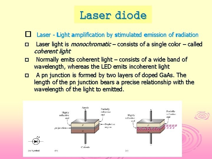
Laser diode Laser - Light amplification by stimulated emission of radiation Laser light is monochromatic – consists of a single color – called coherent light Normally emits coherent light – consists of a wide band of wavelength, whereas the LED emits incoherent light A pn junction is formed by two layers of doped Ga. As. The length of the pn junction bears a precise relationship with the wavelength of the light to emitted.

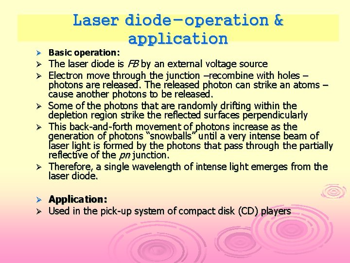
Laser diode-operation & application Ø Ø Ø Ø Basic operation: The laser diode is FB by an external voltage source Electron move through the junction –recombine with holes – photons are released. The released photon can strike an atoms – cause another photons to be released. Some of the photons that are randomly drifting within the depletion region strike the reflected surfaces perpendicularly This back-and-forth movement of photons increase as the generation of photons “snowballs” until a very intense beam of laser light is formed by the photons that pass through the partially reflective of the pn junction. Therefore, a single wavelength of intense light emerges from the laser diode. Application: Used in the pick-up system of compact disk (CD) players

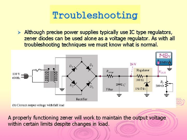
Troubleshooting Ø Although precise power supplies typically use IC type regulators, zener diodes can be used alone as a voltage regulator. As with all troubleshooting techniques we must know what is normal. A properly functioning zener will work to maintain the output voltage within certain limits despite changes in load.

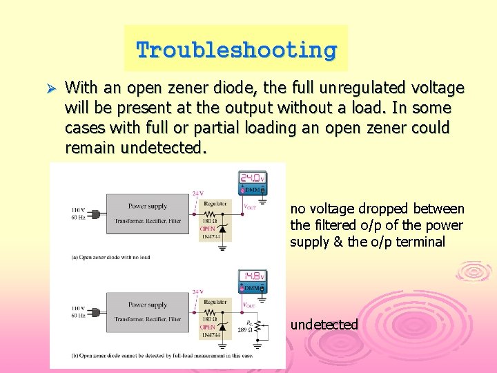
Troubleshooting Ø With an open zener diode, the full unregulated voltage will be present at the output without a load. In some cases with full or partial loading an open zener could remain undetected. no voltage dropped between the filtered o/p of the power supply & the o/p terminal undetected

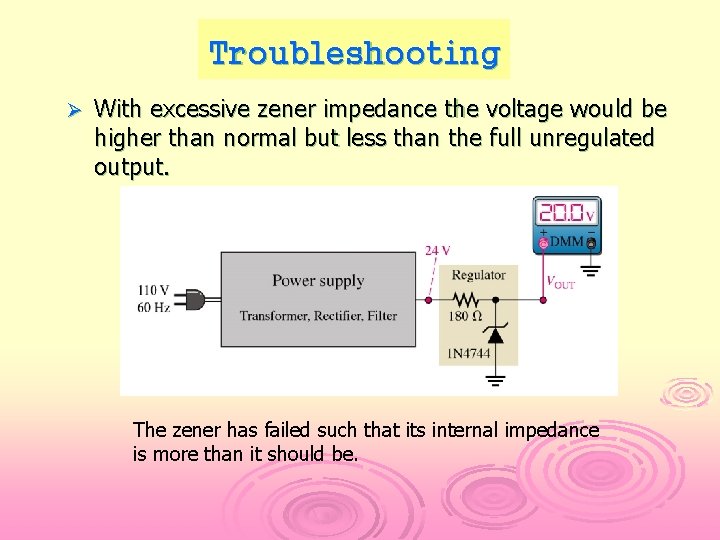
Troubleshooting Ø With excessive zener impedance the voltage would be higher than normal but less than the full unregulated output. The zener has failed such that its internal impedance is more than it should be.

Summary Ø The zener diode operates in reverse breakdown. Ø A zener diode maintains a nearly constant voltage across its terminals over a specified range of currents. Ø Line regulation is the maintenance of a specific voltage with changing input voltages. Ø Load regulation is the maintenance of a specific voltage for different loads. Ø There are other diode types used for specific RF purposes such as varactor diodes (variable capacitance), Schottky diodes (high speed switching), and PIN diodes (microwave attenuation and switching).

Summary Ø Light emitting diodes (LED) emit either infrared or visible light when forward-biased. Ø Photodiodes exhibit an increase in reverse current with light intensity. Ø The laser diode emits a monochromatic light