CHAPTER 3 PART 1 GENERAL SEMICONDUCTOR PACKAGING PROCESS

- Slides: 47

CHAPTER 3 PART 1 GENERAL SEMICONDUCTOR PACKAGING PROCESS FLOW DMT 243 PACKAGING ELECTRONICS

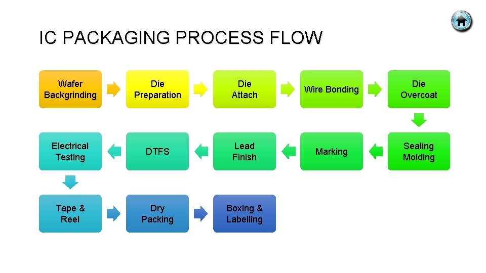
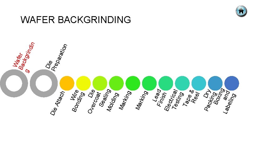
CONTENTS § § § § Wafer Backgrinding. Die Preparation. Die Attach. Wire Bonding. Die Overcoat. Molding. Sealing. Marking. DTFS. Lead Finish. Electrical Testing. Tape & Reel. Dry Packing. Boxing and Labeling.

INTRODUCTION § The integrated circuit, whatever be its level of complexity, will have to be packaged for it to be used in an electronic system. § The silicon chip has to be protected from the environment, electrical connections have to be created to the external world (next level of packaging), and it has to be ensured that the heat generated is effectively dissipated. All these requirements have to be met without significantly reducing the performance of the integrated circuit.

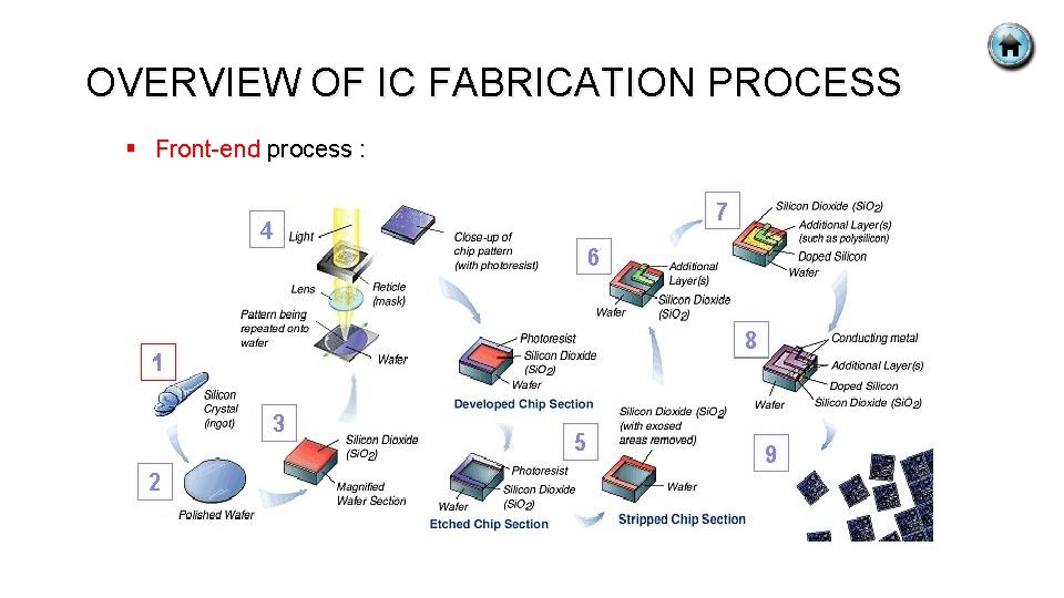
OVERVIEW OF IC FABRICATION PROCESS § Front-end process :

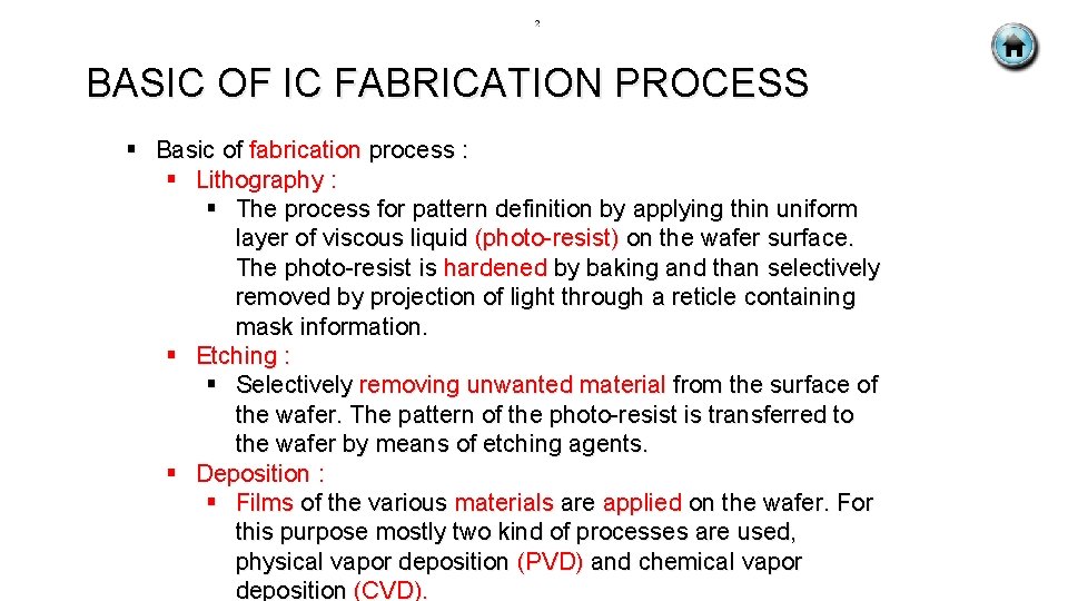
BASIC OF IC FABRICATION PROCESS § Basic of fabrication process : § Lithography : § The process for pattern definition by applying thin uniform layer of viscous liquid (photo-resist) on the wafer surface. The photo-resist is hardened by baking and than selectively removed by projection of light through a reticle containing mask information. § Etching : § Selectively removing unwanted material from the surface of the wafer. The pattern of the photo-resist is transferred to the wafer by means of etching agents. § Deposition : § Films of the various materials are applied on the wafer. For this purpose mostly two kind of processes are used, physical vapor deposition (PVD) and chemical vapor deposition (CVD).

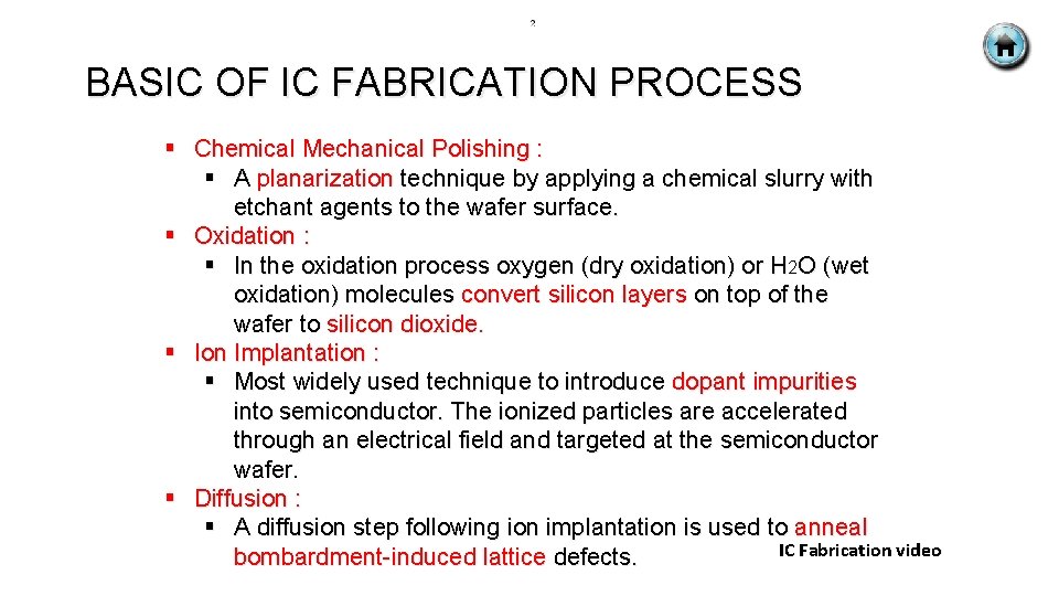
BASIC OF IC FABRICATION PROCESS § Chemical Mechanical Polishing : § A planarization technique by applying a chemical slurry with etchant agents to the wafer surface. § Oxidation : § In the oxidation process oxygen (dry oxidation) or H 2 O (wet oxidation) molecules convert silicon layers on top of the wafer to silicon dioxide. § Ion Implantation : § Most widely used technique to introduce dopant impurities into semiconductor. The ionized particles are accelerated through an electrical field and targeted at the semiconductor wafer. § Diffusion : § A diffusion step following ion implantation is used to anneal IC Fabrication video bombardment-induced lattice defects.

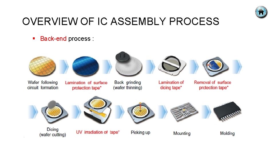
OVERVIEW OF IC ASSEMBLY PROCESS § Back-end process :

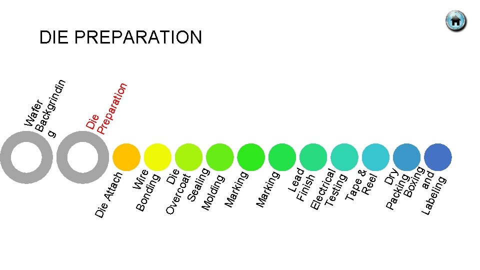
IC PACKAGING PROCESS FLOW Wafer Backgrinding Die Preparation Die Attach Wire Bonding Die Overcoat Electrical Testing DTFS Lead Finish Marking Sealing Molding Tape & Reel Dry Packing Boxing & Labelling

Pa Dry cki n Bo g xin g Lab and elin g Lea Fin d ish Ele ctri Tes cal ting Tap e& Re el Ma rkin g Bo Wire ndi ng Ov erc Die oat Se alin g Mo ldin g Ma rkin g Die Att ach Die Pre par atio n Wa Ba fer g ckgrin din WAFER BACKGRINDING

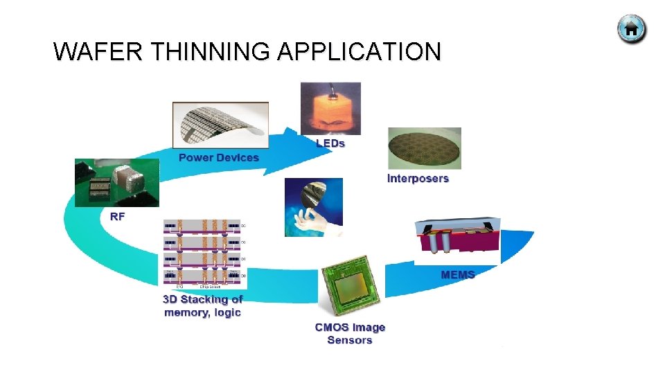
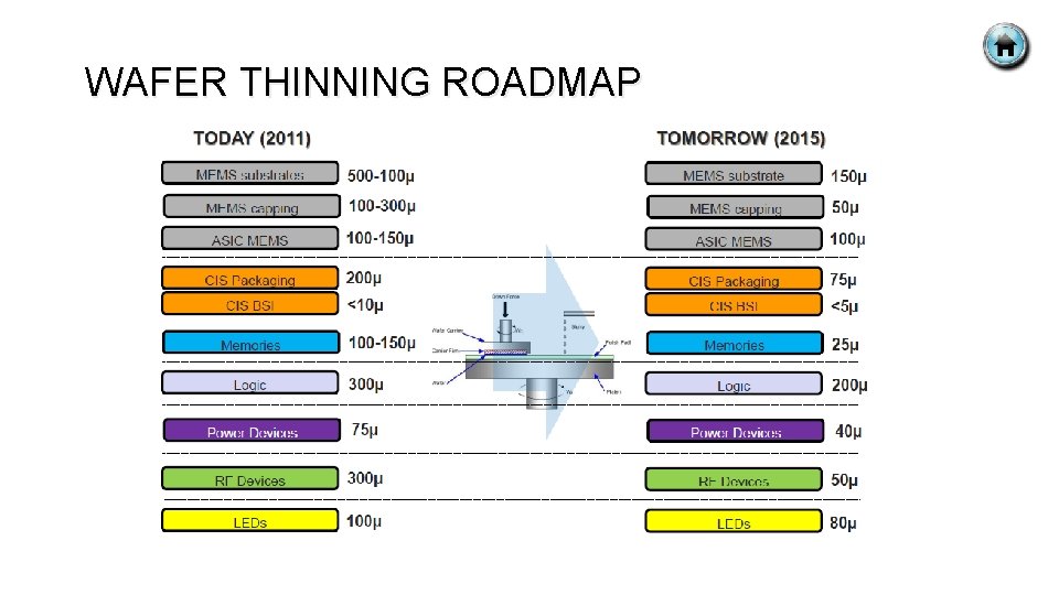
WAFER BACKGRINDING § Process of grinding the backside of the wafer to get the correct wafer thickness prior to assembly. Also referred to as ‘wafer thinning’. § Wafer back grinding has not always been necessary, but the drive to make packages thinner and thinner has made it indispensable. Most package types in the semiconductor industry today would require a wafer thickness ranging from 8 mils (~200 µm) to 20 mils (~500 µm). Stacked die technology would require less than 100 µm. § A thinner wafer allows for better heat removal, lower electrical resistance through the substrate and thinner packages, thus help to improve reliability. § In MEMS, wafer thinning allows for easier formation of thru wafer holes when combined with CMP double sided processing. BG video

WAFER BACKGRINDING

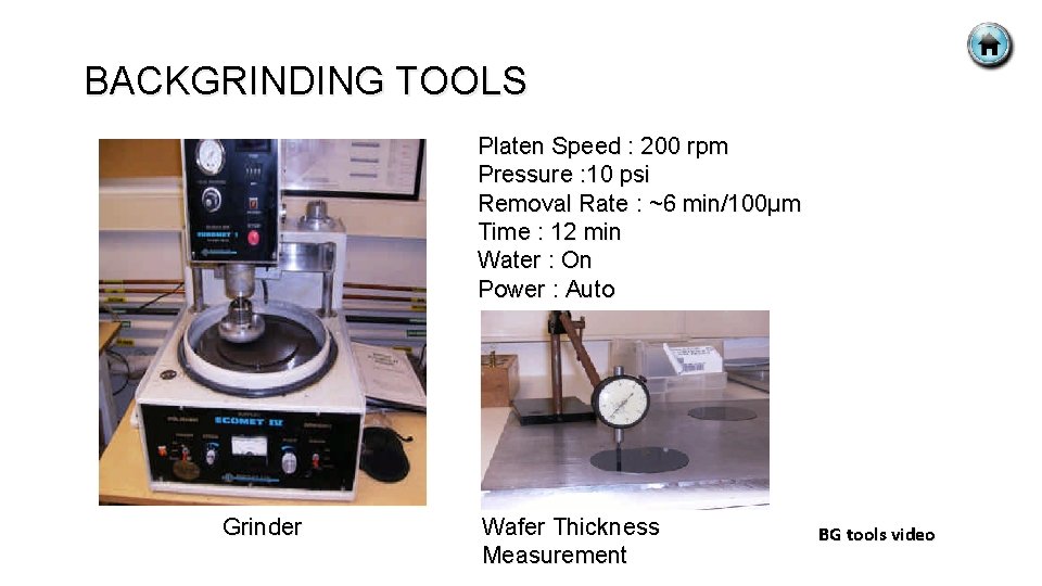
BACKGRINDING TOOLS Platen Speed : 200 rpm Pressure : 10 psi Removal Rate : ~6 min/100μm Time : 12 min Water : On Power : Auto Grinder Wafer Thickness Measurement BG tools video

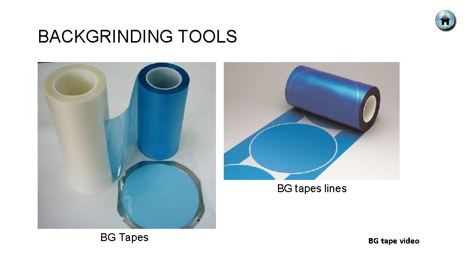
BACKGRINDING TOOLS BG tapes lines BG Tapes BG tape video

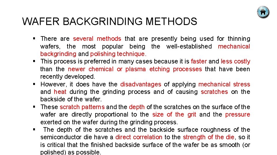
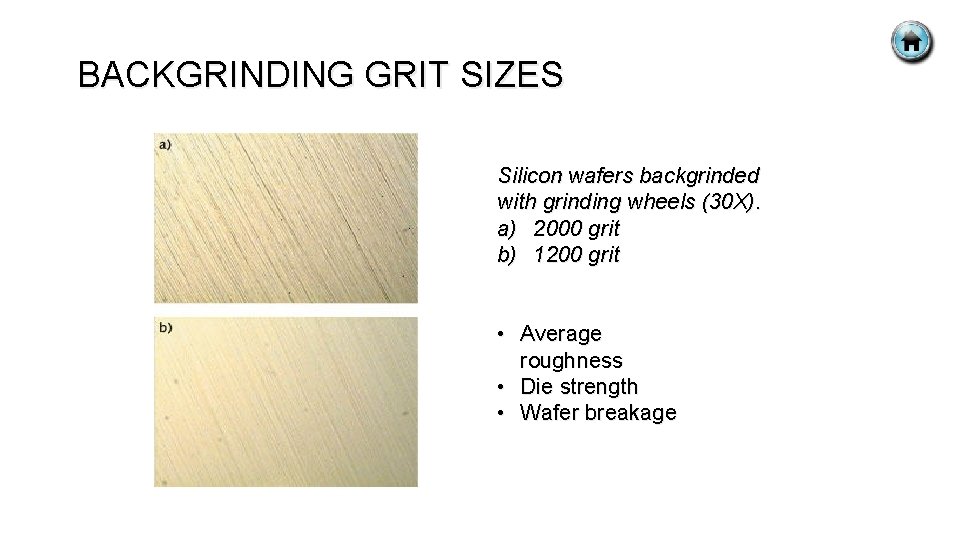
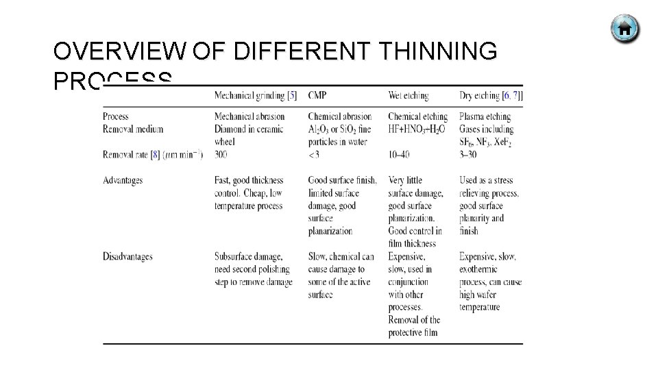
WAFER BACKGRINDING METHODS § There are several methods that are presently being used for thinning wafers, the most popular being the well-established mechanical backgrinding and polishing technique. § This process is preferred in many cases because it is faster and less costly than the newer chemical or plasma etching processes that have been recently developed. § However, it does have the disadvantages of applying mechanical stress and heat during the grinding process and of causing scratches on the backside of the wafer. § These scratch patterns and the depth of the scratches on the surface of the wafer are directly proportional to the size of the grit and the pressure exerted on the wafer during the grinding process. § The depth of the scratches and the backside surface roughness of the semiconductor die have a direct correlation to the strength of the die, so it is critical that the finished backside surface of the wafer be as smooth (or polished) as possible.

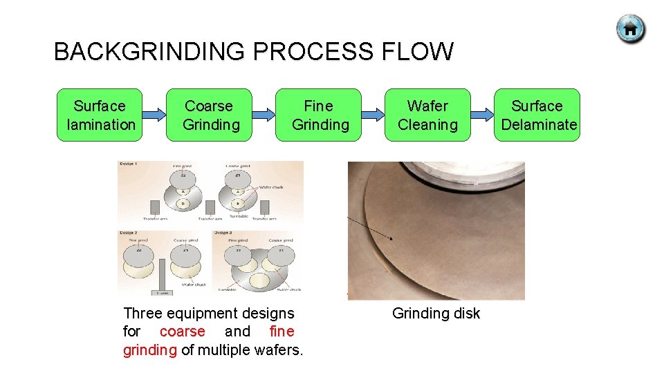
BACKGRINDING PROCESS FLOW Surface lamination Coarse Grinding Fine Grinding Three equipment designs for coarse and fine grinding of multiple wafers. Wafer Cleaning Grinding disk Surface Delaminate

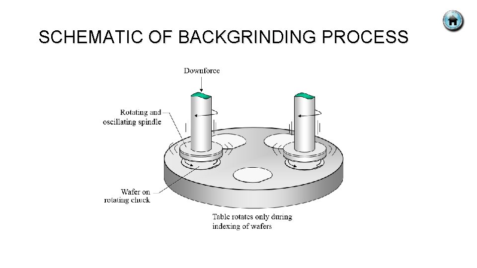
SCHEMATIC OF BACKGRINDING PROCESS

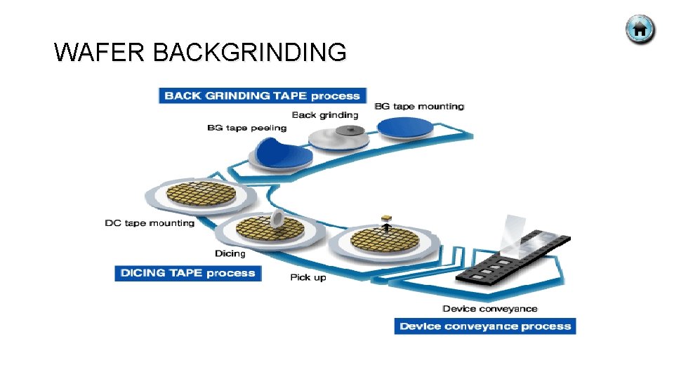
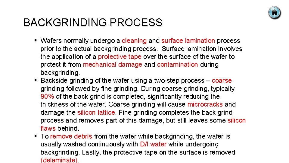
BACKGRINDING PROCESS § Wafers normally undergo a cleaning and surface lamination process prior to the actual backgrinding process. Surface lamination involves the application of a protective tape over the surface of the wafer to protect it from mechanical damage and contamination during backgrinding. § Backside grinding of the wafer using a two-step process – coarse grinding followed by fine grinding. During coarse grinding, typically 90% of the back grind is completed, significantly reducing the thickness of the wafer. Coarse grinding will cause microcracks and damage the silicon lattice. Fine grinding completes the back grind process and removes part of this damage, but still leaves some silicon flaws behind. § To remove debris from the wafer while backgrinding, the wafer is usually washed continuously with D/I water while undergoing backgrinding. Lastly, the protective tape on the surface is removed (delaminate).

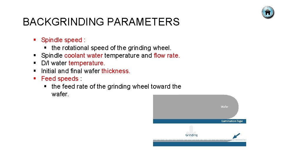
BACKGRINDING PARAMETERS § Spindle speed : § the rotational speed of the grinding wheel. § Spindle coolant water temperature and flow rate. § D/I water temperature. § Initial and final wafer thickness. § Feed speeds : § the feed rate of the grinding wheel toward the wafer.

BACKGRINDING GRIT SIZES Silicon wafers backgrinded with grinding wheels (30 X). a) 2000 grit b) 1200 grit • Average roughness • Die strength • Wafer breakage

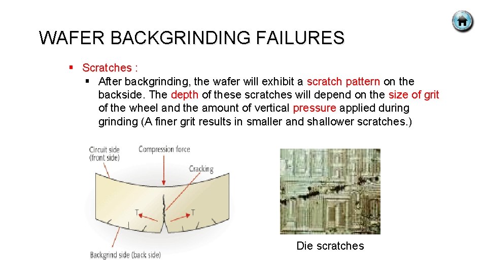
WAFER BACKGRINDING FAILURES § Scratches : § After backgrinding, the wafer will exhibit a scratch pattern on the backside. The depth of these scratches will depend on the size of grit of the wheel and the amount of vertical pressure applied during grinding (A finer grit results in smaller and shallower scratches. ) Die scratches

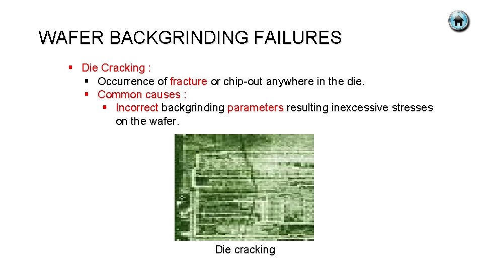
WAFER BACKGRINDING FAILURES § Die Cracking : § Occurrence of fracture or chip-out anywhere in the die. § Common causes : § Incorrect backgrinding parameters resulting inexcessive stresses on the wafer. Die cracking

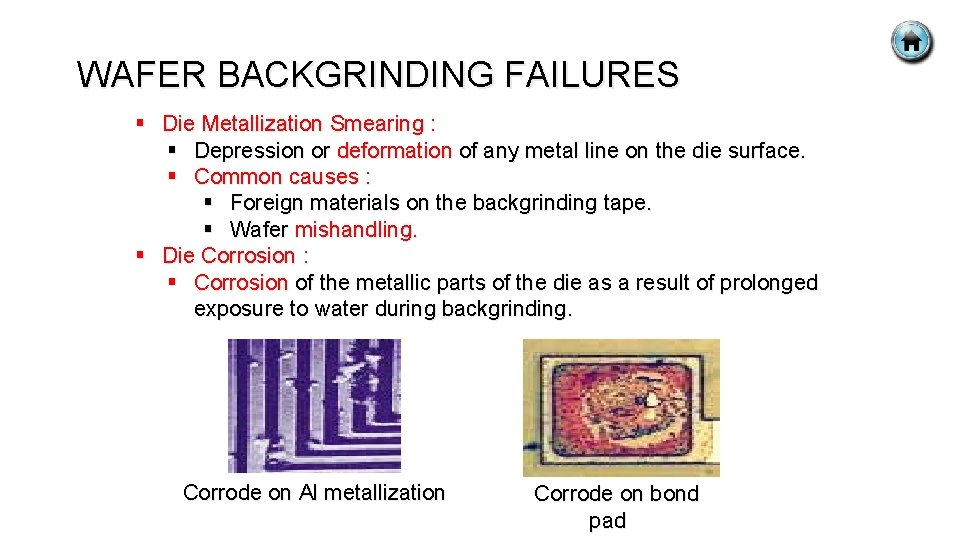
WAFER BACKGRINDING FAILURES § Die Metallization Smearing : § Depression or deformation of any metal line on the die surface. § Common causes : § Foreign materials on the backgrinding tape. § Wafer mishandling. § Die Corrosion : § Corrosion of the metallic parts of the die as a result of prolonged exposure to water during backgrinding. Corrode on Al metallization Corrode on bond pad

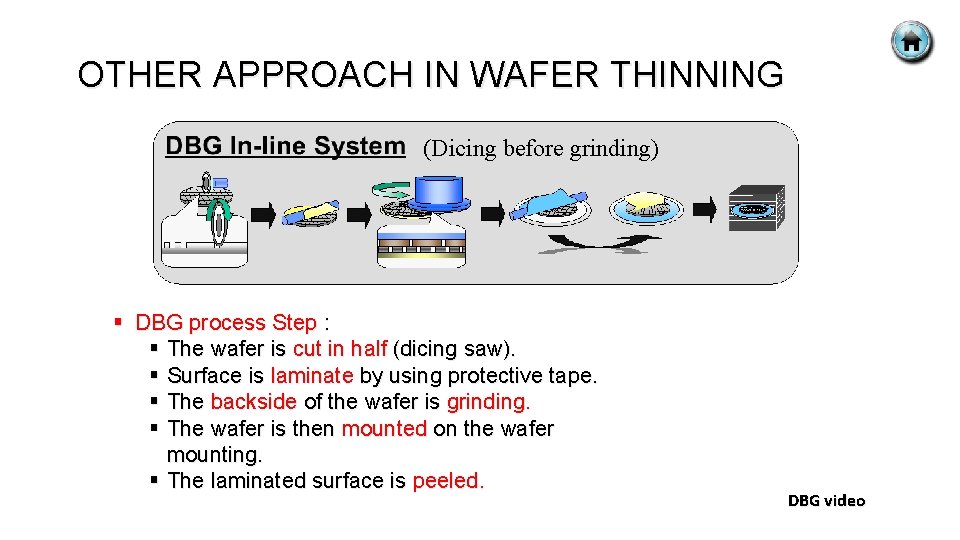
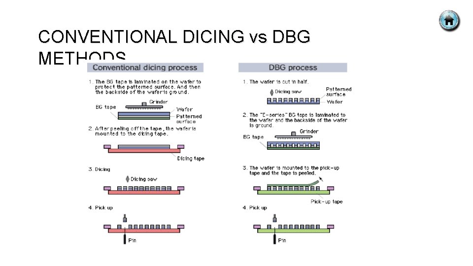
OTHER APPROACH IN WAFER THINNING (Dicing before grinding) § DBG process Step : § The wafer is cut in half (dicing saw). § Surface is laminate by using protective tape. § The backside of the wafer is grinding. § The wafer is then mounted on the wafer mounting. § The laminated surface is peeled. DBG video

CONVENTIONAL DICING vs DBG METHODS

BREAK TIME § Take a sit and relax for 10 MINUTES! VIDEO 1

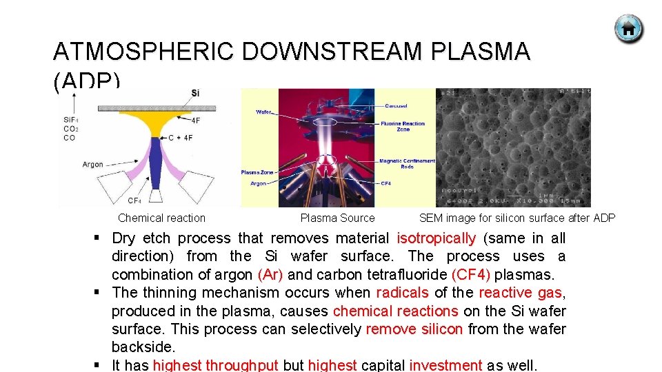
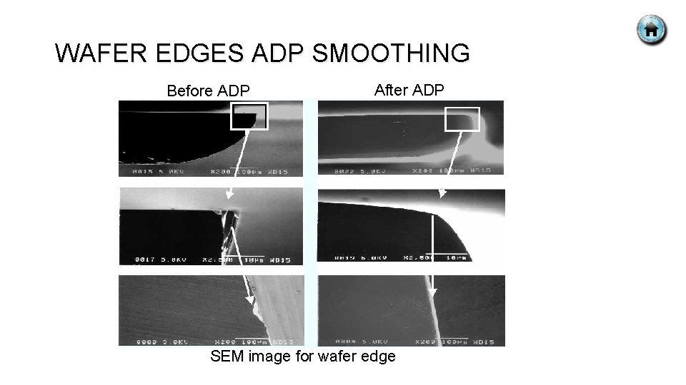
ATMOSPHERIC DOWNSTREAM PLASMA (ADP) Chemical reaction Plasma Source SEM image for silicon surface after ADP § Dry etch process that removes material isotropically (same in all direction) from the Si wafer surface. The process uses a combination of argon (Ar) and carbon tetrafluoride (CF 4) plasmas. § The thinning mechanism occurs when radicals of the reactive gas, produced in the plasma, causes chemical reactions on the Si wafer surface. This process can selectively remove silicon from the wafer backside. § It has highest throughput but highest capital investment as well.

WAFER EDGES ADP SMOOTHING Before ADP After ADP SEM image for wafer edge

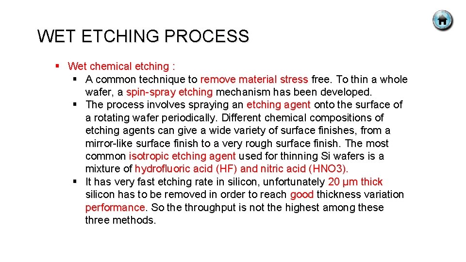
WET ETCHING PROCESS § Wet chemical etching : § A common technique to remove material stress free. To thin a whole wafer, a spin-spray etching mechanism has been developed. § The process involves spraying an etching agent onto the surface of a rotating wafer periodically. Different chemical compositions of etching agents can give a wide variety of surface finishes, from a mirror-like surface finish to a very rough surface finish. The most common isotropic etching agent used for thinning Si wafers is a mixture of hydrofluoric acid (HF) and nitric acid (HNO 3). § It has very fast etching rate in silicon, unfortunately 20 µm thick silicon has to be removed in order to reach good thickness variation performance. So the throughput is not the highest among these three methods.

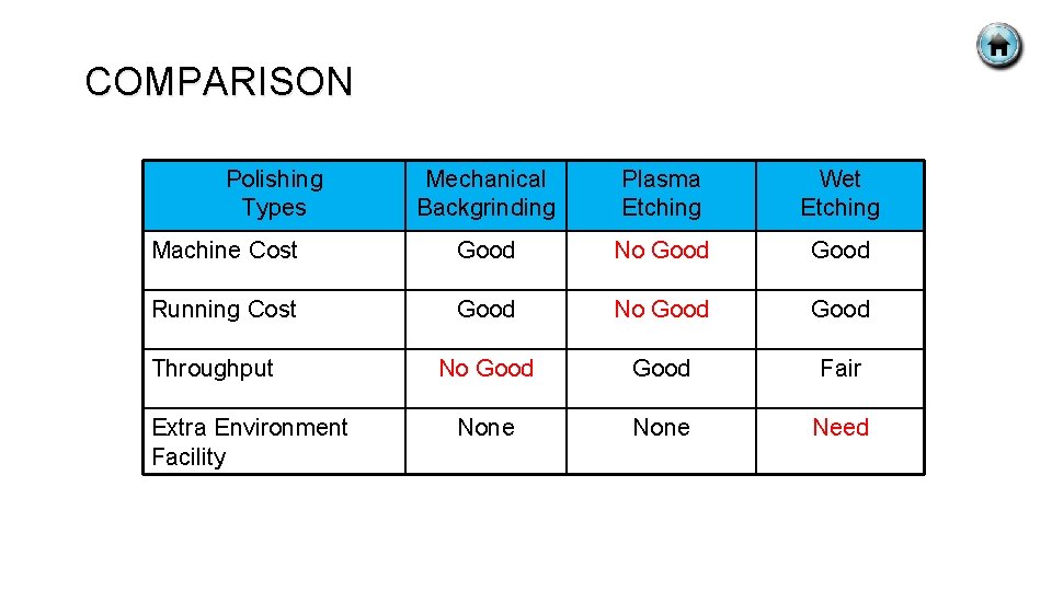
COMPARISON Polishing Types Mechanical Backgrinding Plasma Etching Wet Etching Machine Cost Good No Good Running Cost Good No Good Fair None Need Throughput Extra Environment Facility

OVERVIEW OF DIFFERENT THINNING PROCESS

WAFER THINNING APPLICATION

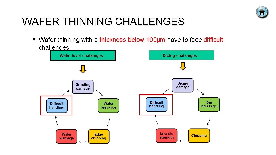
WAFER THINNING CHALLENGES § Wafer thinning with a thickness below 100μm have to face difficult challenges.

WAFER THINNING ROADMAP

Pa Dry cki n Bo g xin g Lab and elin g Lea Fin d ish Ele ctri Tes cal ting Tap e& Re el Ma rkin g Bo Wire ndi ng Ov erc Die oat Se alin g Mo ldin g Ma rkin g Die Att ach Die Pre par atio n Wa Ba fer g ckgrin din DIE PREPARATION

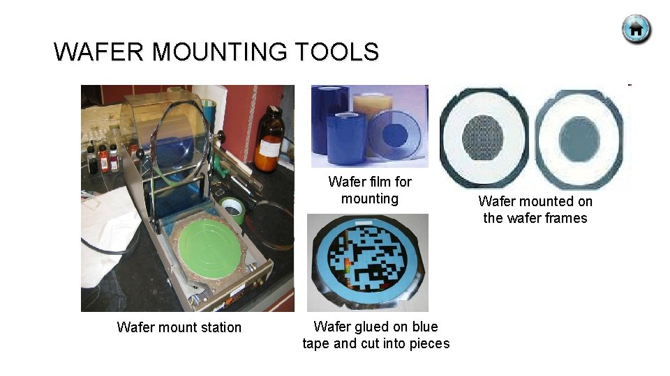
DIE PREPARATION § Die preparation is the process by which the wafer is singulated into individual dice in preparation for assembly. Die preparation consists of two major steps, namely, wafer mounting and wafer saw (diamond scriber/die cutting/dicing). § Wafer mounting is the process of providing support to the wafer to facilitate the processing of the wafer from wafer saw through die attach. § Wafer mounting is performed right before the wafer is cut into separate dice.

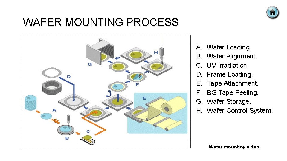
WAFER MOUNTING PROCESS § During wafer mounting process : § The wafer and a wafer frame are simultaneously attached on a wafer or dicing tape. The wafer frame may be made of plastic or metal, but it should be resistant to warping, bending, corrosion, and heat. § The dicing tape (also referred to as a wafer film) is just a PVC sheet with synthetic adhesive on one side to hold both the wafer frame and the wafer. § The adhesive tape on which the wafer is mounted ensures that the individual dice remain firmly in place during dicing (as the process of cutting the wafer). § The following concerns must be prevented : wafer cracking or breakage, bubble trapping on the adhesive side of the tape, scratches on the active side of the wafer, and non-uniform tape tension which can result in tape wrinkles.

WAFER MOUNTING PROCESS A. B. C. D. E. F. G. H. Wafer Loading. Wafer Alignment. UV Irradiation. Frame Loading. Tape Attachment. BG Tape Peeling. Wafer Storage. Wafer Control System. Wafer mounting video

WAFER MOUNTING TOOLS Wafer film for mounting Wafer mount station Wafer glued on blue tape and cut into pieces Wafer mounted on the wafer frames

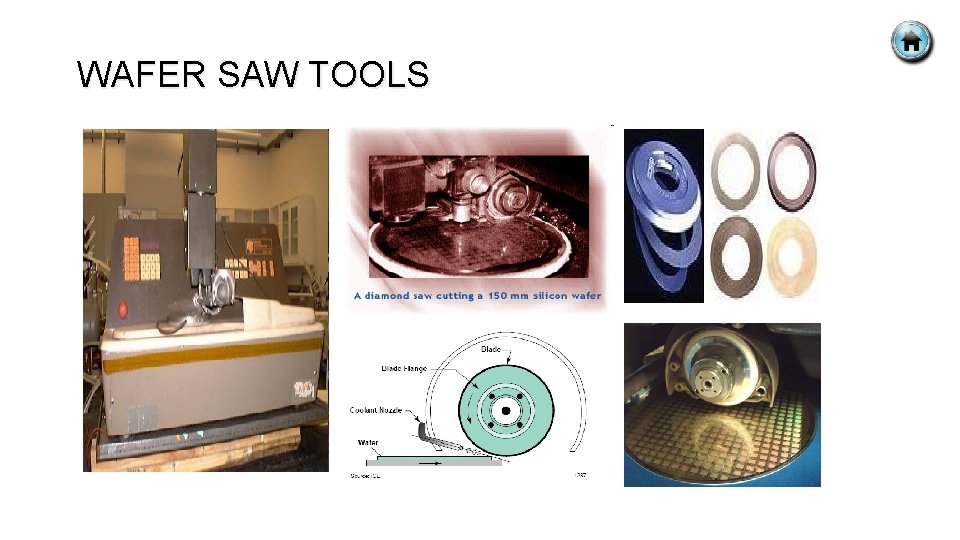
WAFER SAW § Wafer saw or die cutting or dicing is a process of reducing a wafer containing multiple identical integrated circuits to dice each containing one of those circuits. § During this process, a wafer with up to thousands of circuits is cut into individual pieces, each called a die. § In between the functional parts of the circuits, a thin non-functional spacing is foreseen where a saw can safely cut the wafer without damaging the circuit. § This spacing is called the scribe or saw street. The width of the scribe is very small, typically around 100 μm. A very thin and accurate saw is therefore needed to cut the wafer into pieces. Usually the dicing is performed with a water-cooled circular saw with diamond-tipped teeth. Wafer saw video

WAFER SAW TOOLS

WAFER SAW PROCESS § Wafer saw follows wafer mounting step that actually cuts the wafer into individual dice for assembly in IC packages. § The wafer saw process consists of the following steps : § The frame-mounted wafer is automatically aligned into position for cutting. § The wafer is then cut through its thickness according to the programmed die dimensions using a resin-bonded diamond wheel rotating at a very high rpm. § The wafer goes through a cleaning process using high pressure DI water sprayed on the rotating work piece and then dried by airblowing.

WAFER SAW PARAMETERS § Important parameters for consideration during wafer saw included : § Cut mode (direction and manner of cutting). § Feed speed (speed at which the wafer is being introduced to the blade). § Spindle rev (speed of revolution of the cutting wheel). § Blade height. § Cutting water flow. § Important parameters for the washing step include the following: § Wash time. § Wash rpm. § Di water pressure. § Dry time. § Dry rpm. § Temperature. § Air flow rate.

DIE PREPARATION FAILURES § Die Lifting : § Detachment of the die from the die pad or cavity. Wafer backside contamination during die preparation may inhibit good adhesion between the die backside and the die attach material. § Common causes : § Contamination on the die pad or cavity. § Excessive die attach voids. § Incomplete die attach coverage. § Inadequate die attach curing.

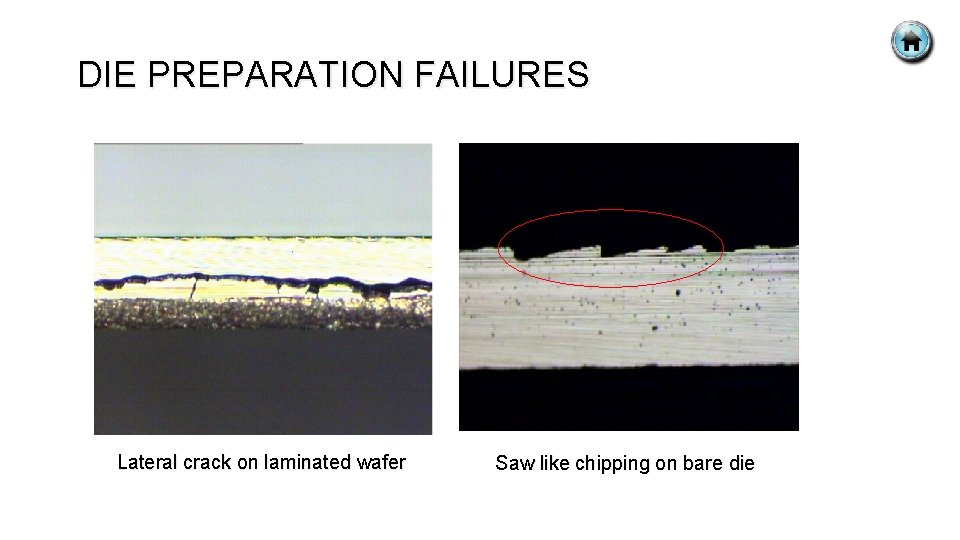
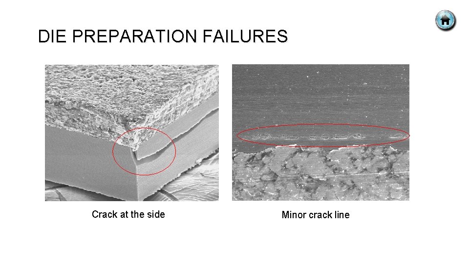
DIE PREPARATION FAILURES § Die Cracking : § Occurrence of fracture anywhere in the die. Incorrect wafer saw and washing parameters can result in microcracks in the wafers, which can propagate into larger die cracks during later stages of the assembly process. § Common causes : § Excessive die attach voids. § Die overhang or insufficient die attach coverage. § Excessive die ejection force on the wafer tape.

DIE PREPARATION FAILURES § Die Contamination : § Contamination of the die surface with silicon dust or foreign material that may be attached either by electrostatic, mechanical, or chemical means. § Common Causes : § Contaminated rinsing water. § Static charge.

DIE PREPARATION FAILURES Lateral crack on laminated wafer Saw like chipping on bare die

DIE PREPARATION FAILURES Crack at the side Minor crack line