Chapter 3 Communication Concepts 3 1 General Considerations
- Slides: 91

Chapter 3 Communication Concepts Ø Ø Ø Ø 3. 1 General Considerations 3. 2 Analog Modulation 3. 3 Digital Modulation 3. 4 Spectral Regrowth 3. 5 Mobile RF Communications 3. 6 Multiple Access Techniques 3. 7 Wireless Standards 3. 8 Appendix I: Differential Phase Shift Keying Behzad Razavi, RF Microelectronics. 1 Prepared by Bo Wen, UCLA

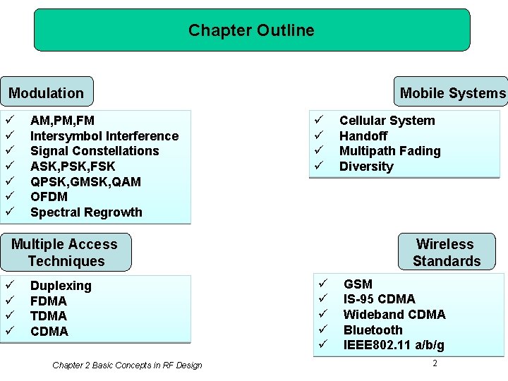
Chapter Outline Mobile Systems Modulation ü ü ü ü AM, PM, FM Intersymbol Interference Signal Constellations ASK, PSK, FSK QPSK, GMSK, QAM OFDM Spectral Regrowth ü ü Multiple Access Techniques ü ü Duplexing FDMA TDMA Chapter 2 Basic Concepts in RF Design Cellular System Handoff Multipath Fading Diversity Wireless Standards ü ü ü GSM IS-95 CDMA Wideband CDMA Bluetooth IEEE 802. 11 a/b/g 2

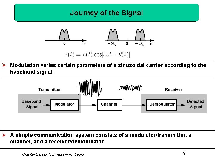
Journey of the Signal Ø Modulation varies certain parameters of a sinusoidal carrier according to the baseband signal. Ø A simple communication system consists of a modulator/transmitter, a channel, and a receiver/demodulator Chapter 2 Basic Concepts in RF Design 3

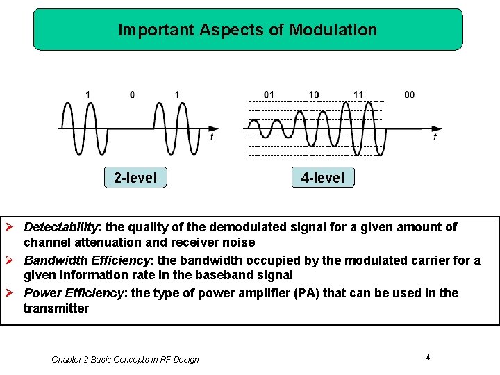
Important Aspects of Modulation 2 -level 4 -level Ø Detectability: the quality of the demodulated signal for a given amount of channel attenuation and receiver noise Ø Bandwidth Efficiency: the bandwidth occupied by the modulated carrier for a given information rate in the baseband signal Ø Power Efficiency: the type of power amplifier (PA) that can be used in the transmitter Chapter 2 Basic Concepts in RF Design 4

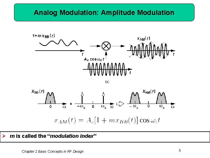
Analog Modulation: Amplitude Modulation Ø m is called the “modulation index” Chapter 2 Basic Concepts in RF Design 5

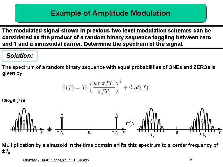
Example of Amplitude Modulation The modulated signal shown in previous two level modulation schemes can be considered as the product of a random binary sequence toggling between zero and 1 and a sinusoidal carrier. Determine the spectrum of the signal. Solution: The spectrum of a random binary sequence with equal probabilities of ONEs and ZEROs is given by Multiplication by a sinusoid in the time domain shifts this spectrum to a center frequency of ± fc Chapter 2 Basic Concepts in RF Design 6

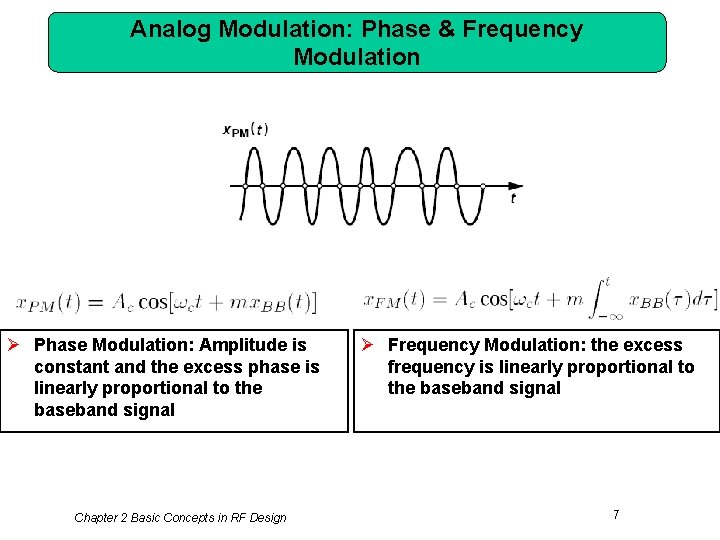
Analog Modulation: Phase & Frequency Modulation Ø Phase Modulation: Amplitude is constant and the excess phase is linearly proportional to the baseband signal Chapter 2 Basic Concepts in RF Design Ø Frequency Modulation: the excess frequency is linearly proportional to the baseband signal 7

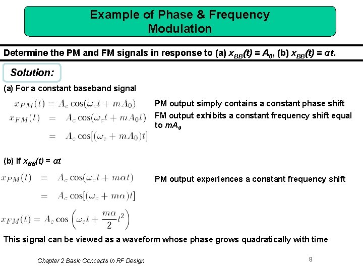
Example of Phase & Frequency Modulation Determine the PM and FM signals in response to (a) x. BB(t) = A 0, (b) x. BB(t) = αt. Solution: (a) For a constant baseband signal PM output simply contains a constant phase shift FM output exhibits a constant frequency shift equal to m. A 0 (b) If x. BB(t) = αt PM output experiences a constant frequency shift This signal can be viewed as a waveform whose phase grows quadratically with time Chapter 2 Basic Concepts in RF Design 8

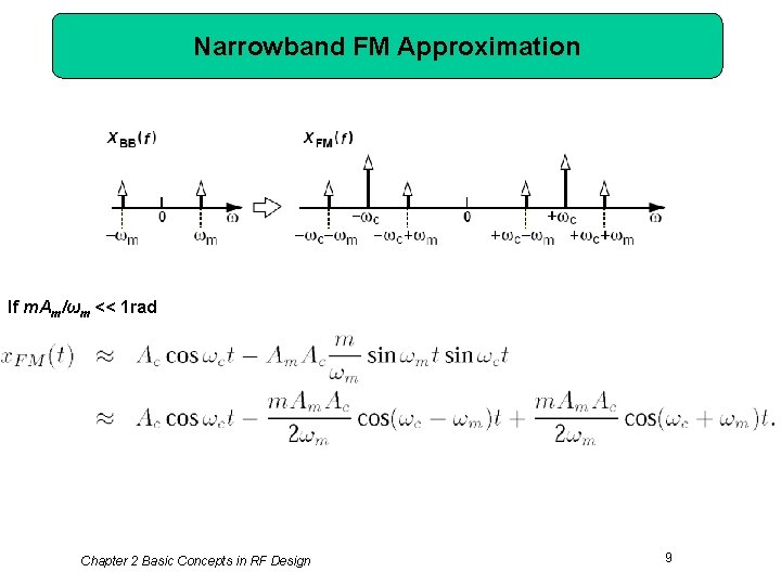
Narrowband FM Approximation If m. Am/ωm << 1 rad Chapter 2 Basic Concepts in RF Design 9

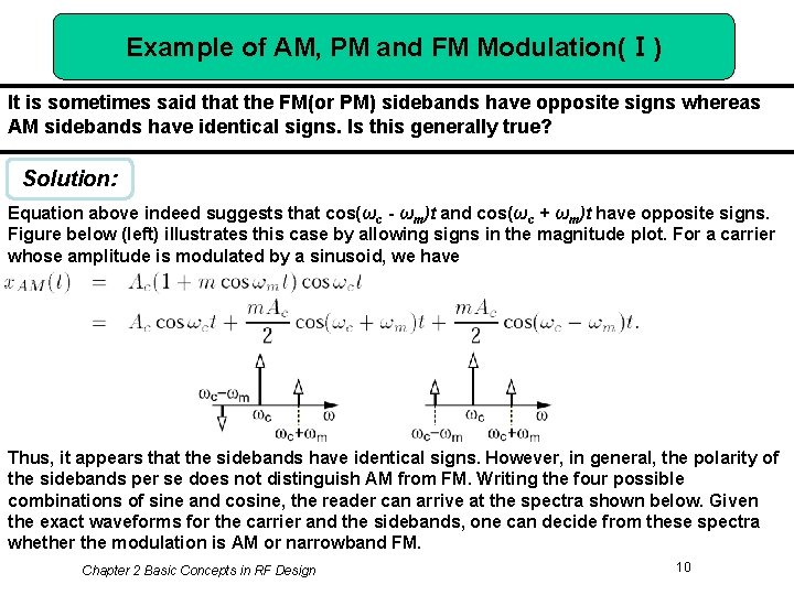
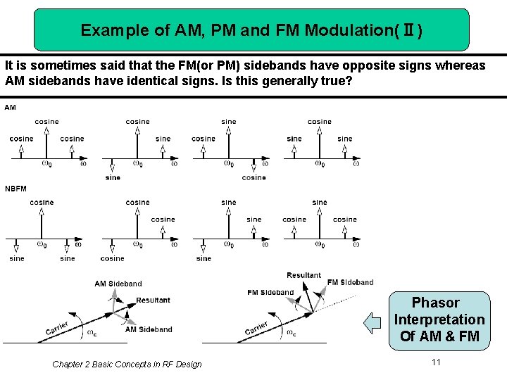
Example of AM, PM and FM Modulation(Ⅰ) It is sometimes said that the FM(or PM) sidebands have opposite signs whereas AM sidebands have identical signs. Is this generally true? Solution: Equation above indeed suggests that cos(ωc - ωm)t and cos(ωc + ωm)t have opposite signs. Figure below (left) illustrates this case by allowing signs in the magnitude plot. For a carrier whose amplitude is modulated by a sinusoid, we have Thus, it appears that the sidebands have identical signs. However, in general, the polarity of the sidebands per se does not distinguish AM from FM. Writing the four possible combinations of sine and cosine, the reader can arrive at the spectra shown below. Given the exact waveforms for the carrier and the sidebands, one can decide from these spectra whether the modulation is AM or narrowband FM. Chapter 2 Basic Concepts in RF Design 10

Example of AM, PM and FM Modulation(Ⅱ) It is sometimes said that the FM(or PM) sidebands have opposite signs whereas AM sidebands have identical signs. Is this generally true? Phasor Interpretation Of AM & FM Chapter 2 Basic Concepts in RF Design 11

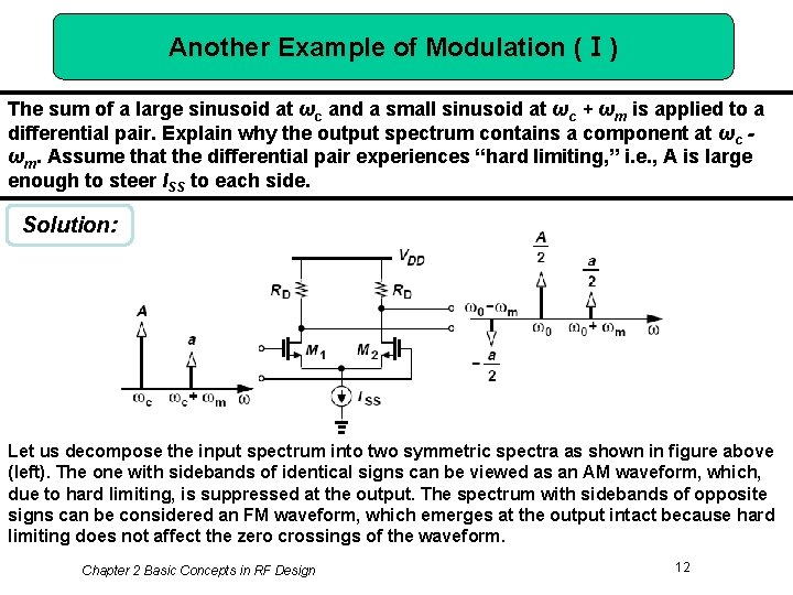
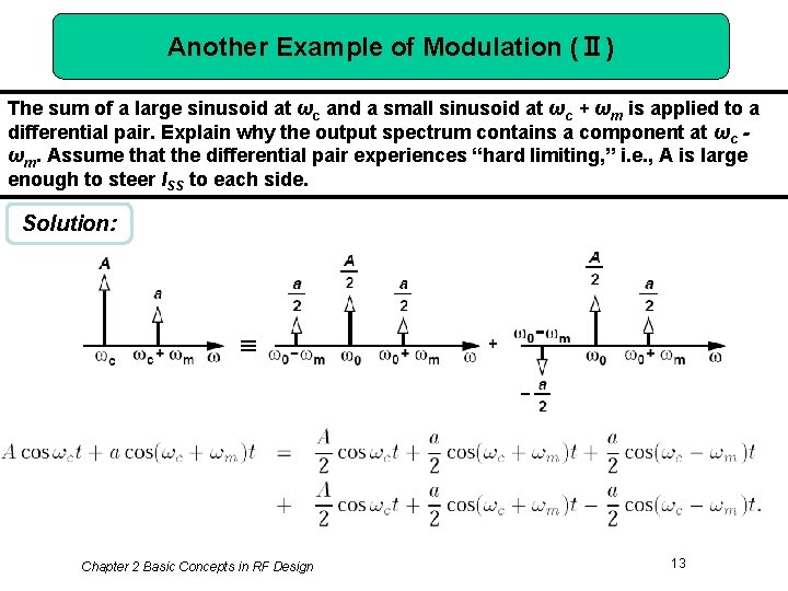
Another Example of Modulation (Ⅰ) The sum of a large sinusoid at ωc and a small sinusoid at ωc + ωm is applied to a differential pair. Explain why the output spectrum contains a component at ωc ωm. Assume that the differential pair experiences “hard limiting, ” i. e. , A is large enough to steer ISS to each side. Solution: Let us decompose the input spectrum into two symmetric spectra as shown in figure above (left). The one with sidebands of identical signs can be viewed as an AM waveform, which, due to hard limiting, is suppressed at the output. The spectrum with sidebands of opposite signs can be considered an FM waveform, which emerges at the output intact because hard limiting does not affect the zero crossings of the waveform. Chapter 2 Basic Concepts in RF Design 12

Another Example of Modulation (Ⅱ) The sum of a large sinusoid at ωc and a small sinusoid at ωc + ωm is applied to a differential pair. Explain why the output spectrum contains a component at ωc ωm. Assume that the differential pair experiences “hard limiting, ” i. e. , A is large enough to steer ISS to each side. Solution: Chapter 2 Basic Concepts in RF Design 13

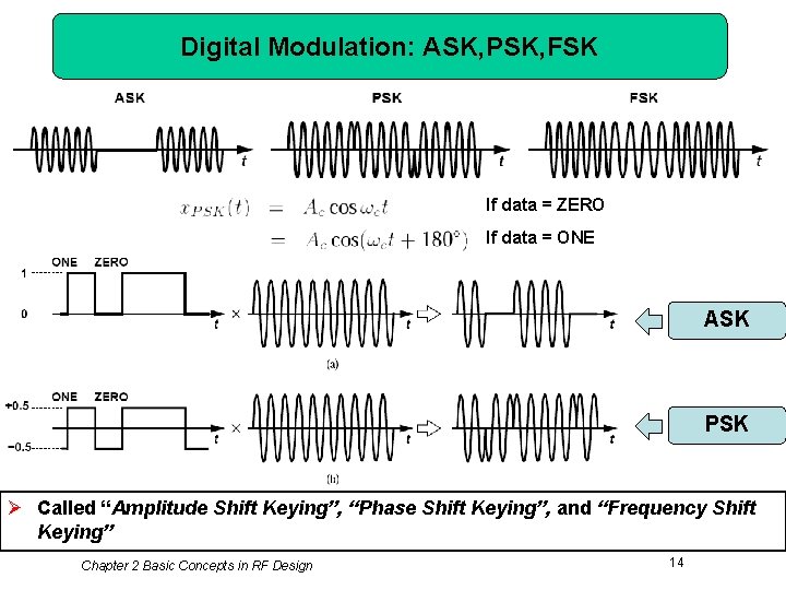
Digital Modulation: ASK, PSK, FSK If data = ZERO If data = ONE ASK PSK Ø Called “Amplitude Shift Keying”, “Phase Shift Keying”, and “Frequency Shift Keying” Chapter 2 Basic Concepts in RF Design 14

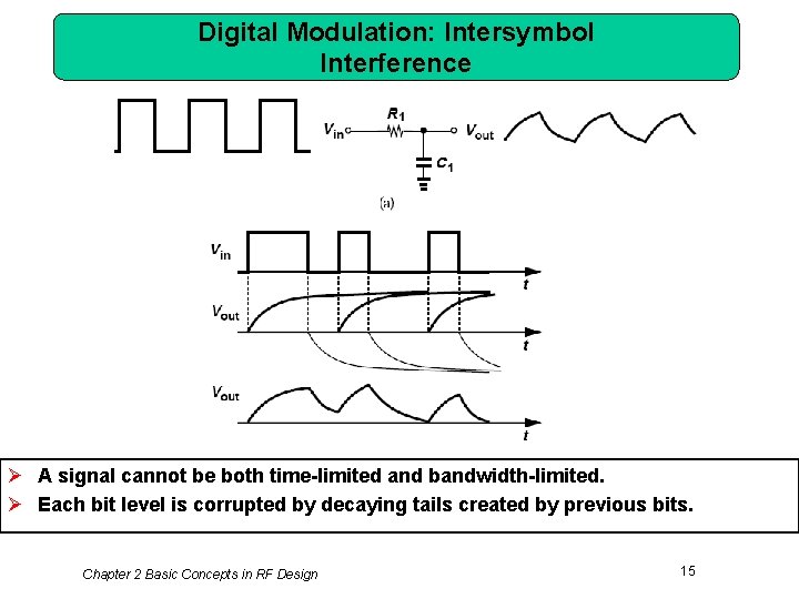
Digital Modulation: Intersymbol Interference Ø A signal cannot be both time-limited and bandwidth-limited. Ø Each bit level is corrupted by decaying tails created by previous bits. Chapter 2 Basic Concepts in RF Design 15

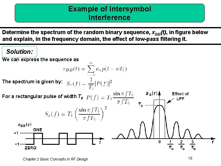
Example of Intersymbol Interference Determine the spectrum of the random binary sequence, x. BB(t), in figure below and explain, in the frequency domain, the effect of low-pass filtering it. Solution: We can express the sequence as The spectrum is given by: For a rectangular pulse of width Tb Chapter 2 Basic Concepts in RF Design 16

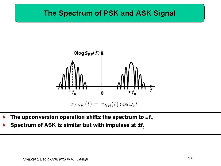
The Spectrum of PSK and ASK Signal Ø The upconversion operation shifts the spectrum to ±fc Ø Spectrum of ASK is similar but with impulses at ±fc Chapter 2 Basic Concepts in RF Design 17

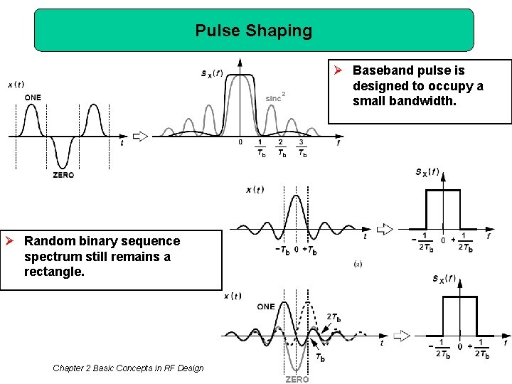
Pulse Shaping Ø Baseband pulse is designed to occupy a small bandwidth. Ø Random binary sequence spectrum still remains a rectangle. Chapter 2 Basic Concepts in RF Design 18

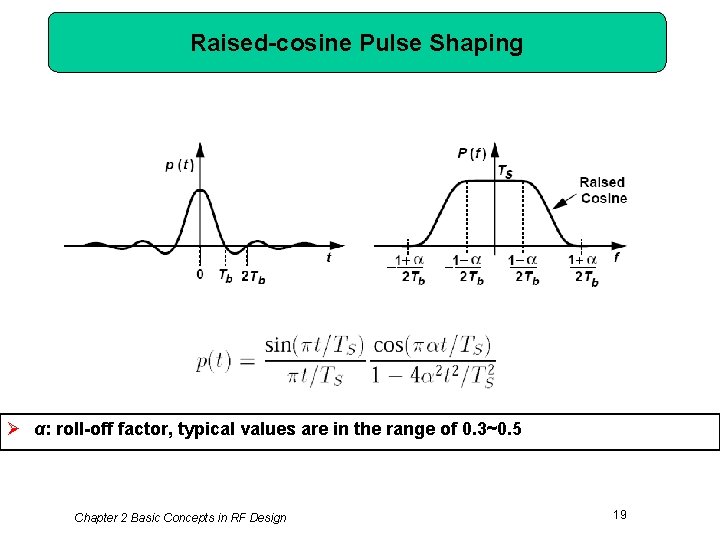
Raised-cosine Pulse Shaping Ø α: roll-off factor, typical values are in the range of 0. 3~0. 5 Chapter 2 Basic Concepts in RF Design 19

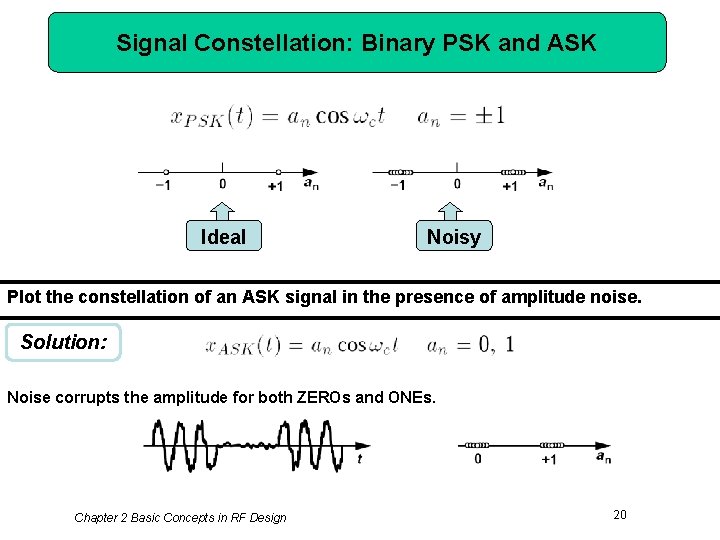
Signal Constellation: Binary PSK and ASK Ideal Noisy Plot the constellation of an ASK signal in the presence of amplitude noise. Solution: Noise corrupts the amplitude for both ZEROs and ONEs. Chapter 2 Basic Concepts in RF Design 20

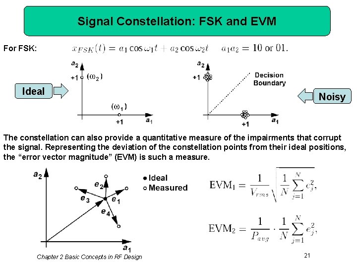
Signal Constellation: FSK and EVM For FSK: Ideal Noisy The constellation can also provide a quantitative measure of the impairments that corrupt the signal. Representing the deviation of the constellation points from their ideal positions, the “error vector magnitude” (EVM) is such a measure. Chapter 2 Basic Concepts in RF Design 21

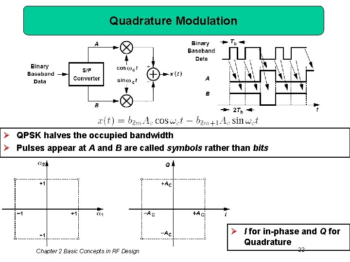
Quadrature Modulation Ø QPSK halves the occupied bandwidth Ø Pulses appear at A and B are called symbols rather than bits Ø I for in-phase and Q for Quadrature Chapter 2 Basic Concepts in RF Design 22

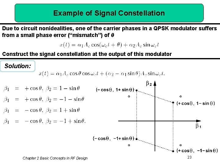
Example of Signal Constellation Due to circuit nonidealities, one of the carrier phases in a QPSK modulator suffers from a small phase error (“mismatch”) of θ Construct the signal constellation at the output of this modulator Solution: Chapter 2 Basic Concepts in RF Design 23

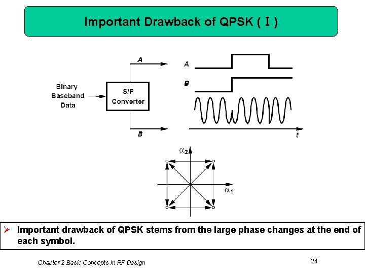
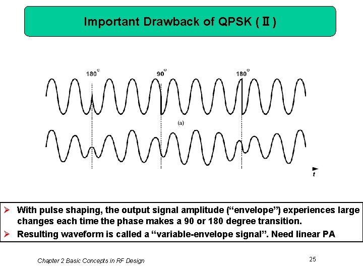
Important Drawback of QPSK (Ⅰ) Ø Important drawback of QPSK stems from the large phase changes at the end of each symbol. Chapter 2 Basic Concepts in RF Design 24

Important Drawback of QPSK (Ⅱ) Ø With pulse shaping, the output signal amplitude (“envelope”) experiences large changes each time the phase makes a 90 or 180 degree transition. Ø Resulting waveform is called a “variable-envelope signal”. Need linear PA Chapter 2 Basic Concepts in RF Design 25

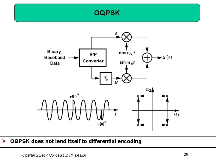
OQPSK Ø OQPSK does not lend itself to differential encoding Chapter 2 Basic Concepts in RF Design 26

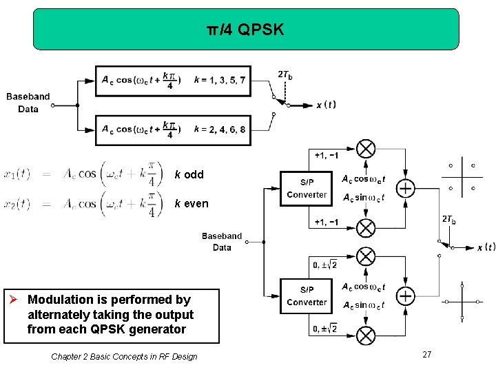
π/4 QPSK k odd k even Ø Modulation is performed by alternately taking the output from each QPSK generator Chapter 2 Basic Concepts in RF Design 27

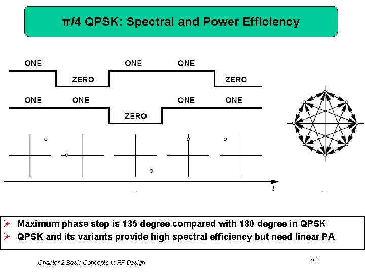
π/4 QPSK: Spectral and Power Efficiency Ø Maximum phase step is 135 degree compared with 180 degree in QPSK Ø QPSK and its variants provide high spectral efficiency but need linear PA Chapter 2 Basic Concepts in RF Design 28

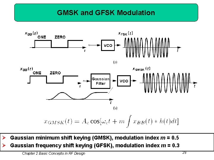
GMSK and GFSK Modulation Ø Gaussian minimum shift keying (GMSK), modulation index m = 0. 5 Ø Gaussian frequency shift keying (GFSK), modulation index m = 0. 3 Chapter 2 Basic Concepts in RF Design 29

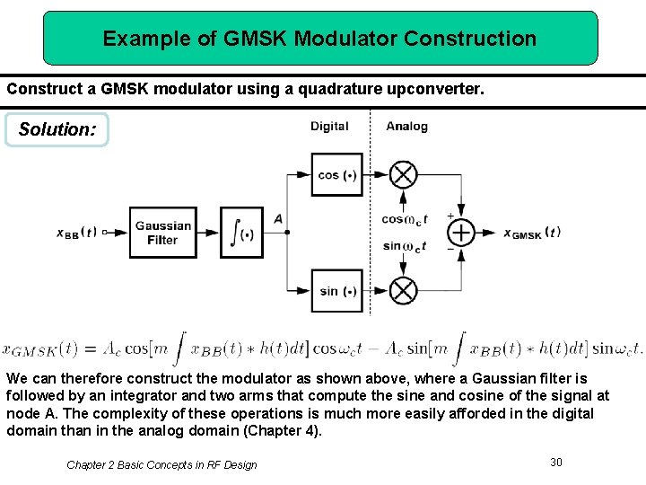
Example of GMSK Modulator Construction Construct a GMSK modulator using a quadrature upconverter. Solution: We can therefore construct the modulator as shown above, where a Gaussian filter is followed by an integrator and two arms that compute the sine and cosine of the signal at node A. The complexity of these operations is much more easily afforded in the digital domain than in the analog domain (Chapter 4). Chapter 2 Basic Concepts in RF Design 30

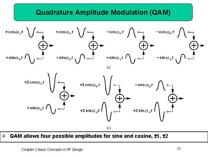
Quadrature Amplitude Modulation (QAM) Ø QAM allows four possible amplitudes for sine and cosine, ± 1, ± 2 Chapter 2 Basic Concepts in RF Design 31

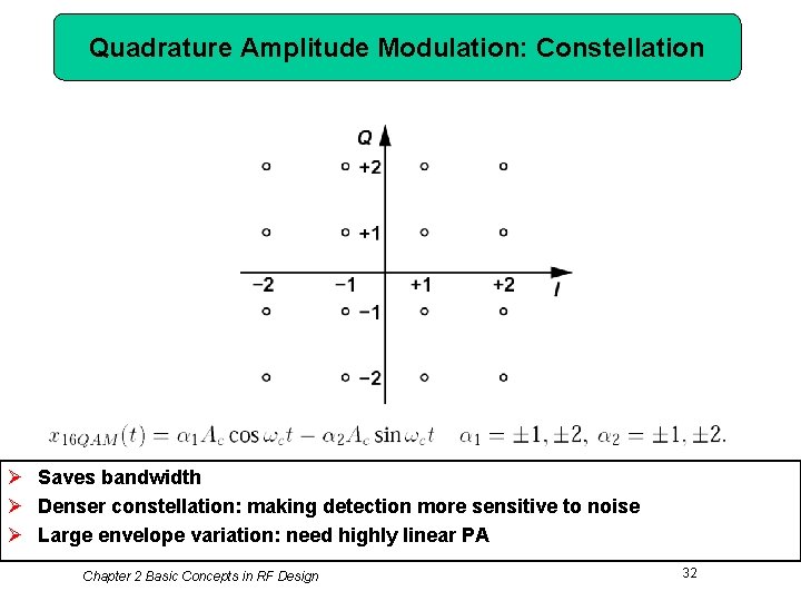
Quadrature Amplitude Modulation: Constellation Ø Saves bandwidth Ø Denser constellation: making detection more sensitive to noise Ø Large envelope variation: need highly linear PA Chapter 2 Basic Concepts in RF Design 32

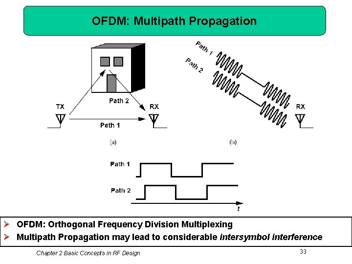
OFDM: Multipath Propagation Ø OFDM: Orthogonal Frequency Division Multiplexing Ø Multipath Propagation may lead to considerable intersymbol interference Chapter 2 Basic Concepts in RF Design 33

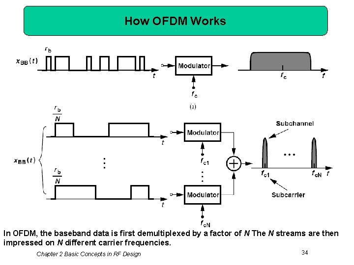
How OFDM Works In OFDM, the baseband data is first demultiplexed by a factor of N The N streams are then impressed on N different carrier frequencies. Chapter 2 Basic Concepts in RF Design 34

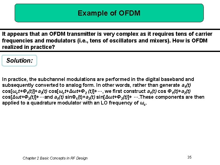
Example of OFDM It appears that an OFDM transmitter is very complex as it requires tens of carrier frequencies and modulators (i. e. , tens of oscillators and mixers). How is OFDM realized in practice? Solution: In practice, the subchannel modulations are performed in the digital baseband subsequently converted to analog form. In other words, rather than generate a 1(t) cos[ωct+Φ 1(t)]+a 2(t) cos[ωct+Δωt+Φ 2 (t)]+···, we first construct a 1(t) cos Φ 1(t)+a 2(t) cos[Δωt+Φ 2(t)]+···and a 1(t) sinΦ 1(t)+a 2(t) sin[Δωt+Φ 2(t)]+ ···. These components are then applied to a quadrature modulator with an LO frequency of ωc. Chapter 2 Basic Concepts in RF Design 35

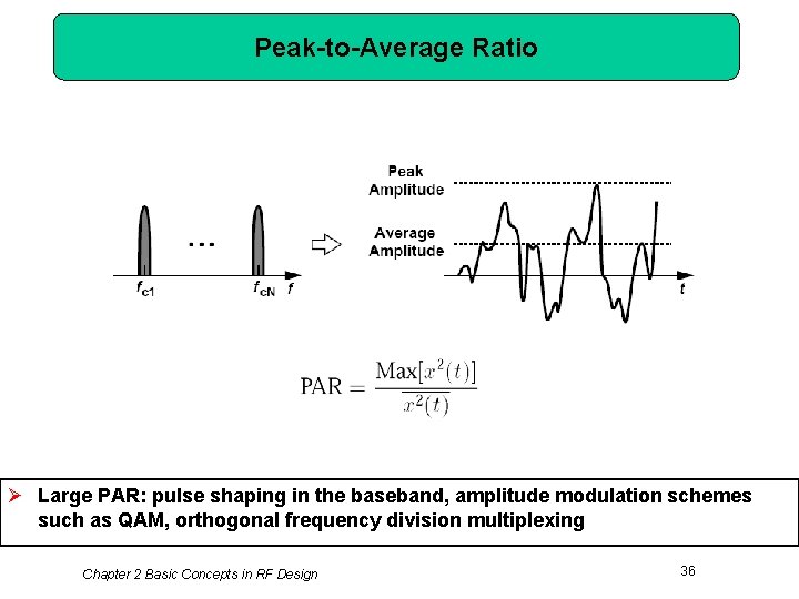
Peak-to-Average Ratio Ø Large PAR: pulse shaping in the baseband, amplitude modulation schemes such as QAM, orthogonal frequency division multiplexing Chapter 2 Basic Concepts in RF Design 36

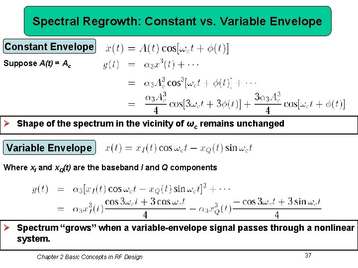
Spectral Regrowth: Constant vs. Variable Envelope Constant Envelope Suppose A(t) = Ac Ø Shape of the spectrum in the vicinity of ωc remains unchanged Variable Envelope Where x. I and x. Q(t) are the baseband I and Q components Ø Spectrum “grows” when a variable-envelope signal passes through a nonlinear system. Chapter 2 Basic Concepts in RF Design 37

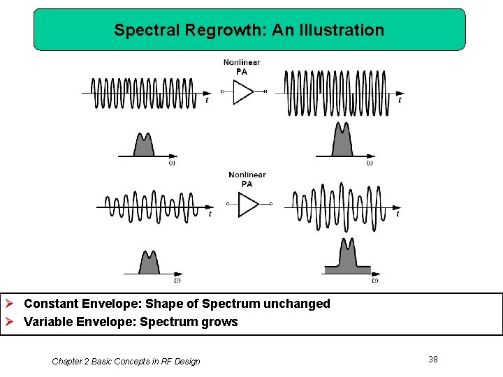
Spectral Regrowth: An Illustration Ø Constant Envelope: Shape of Spectrum unchanged Ø Variable Envelope: Spectrum grows Chapter 2 Basic Concepts in RF Design 38

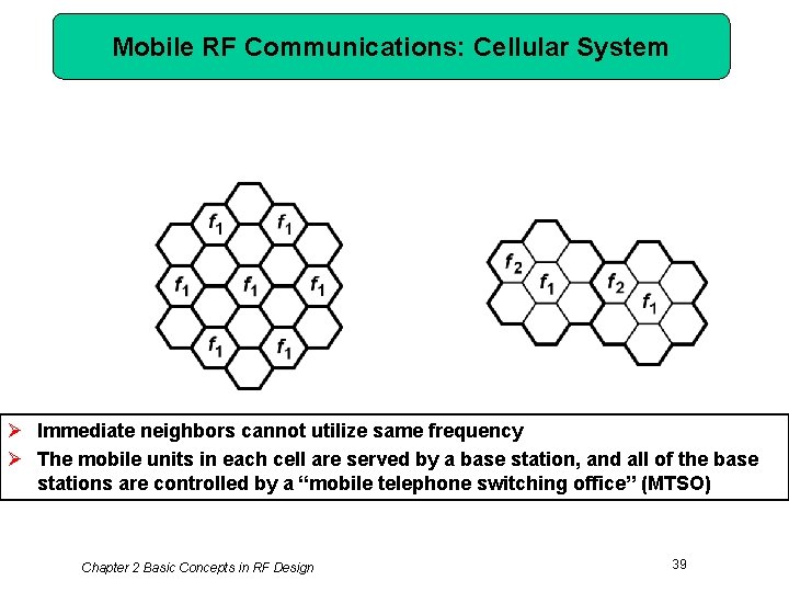
Mobile RF Communications: Cellular System Ø Immediate neighbors cannot utilize same frequency Ø The mobile units in each cell are served by a base station, and all of the base stations are controlled by a “mobile telephone switching office” (MTSO) Chapter 2 Basic Concepts in RF Design 39

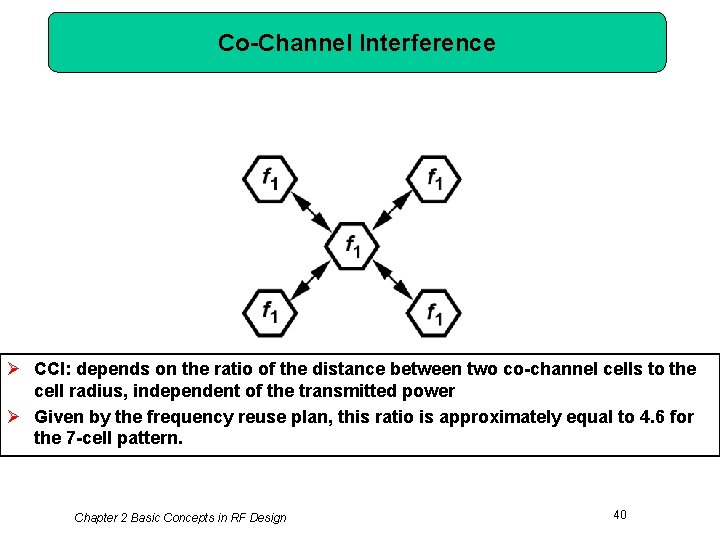
Co-Channel Interference Ø CCI: depends on the ratio of the distance between two co-channel cells to the cell radius, independent of the transmitted power Ø Given by the frequency reuse plan, this ratio is approximately equal to 4. 6 for the 7 -cell pattern. Chapter 2 Basic Concepts in RF Design 40

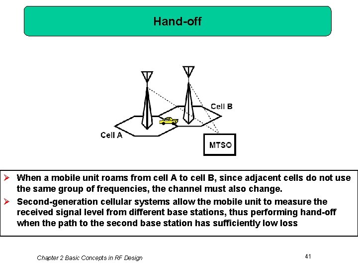
Hand-off Ø When a mobile unit roams from cell A to cell B, since adjacent cells do not use the same group of frequencies, the channel must also change. Ø Second-generation cellular systems allow the mobile unit to measure the received signal level from different base stations, thus performing hand-off when the path to the second base station has sufficiently low loss Chapter 2 Basic Concepts in RF Design 41

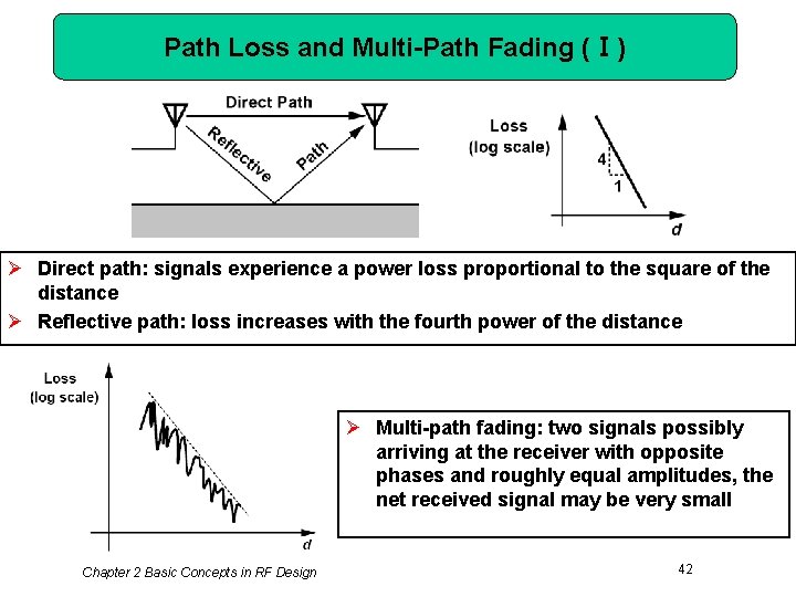
Path Loss and Multi-Path Fading (Ⅰ) Ø Direct path: signals experience a power loss proportional to the square of the distance Ø Reflective path: loss increases with the fourth power of the distance Ø Multi-path fading: two signals possibly arriving at the receiver with opposite phases and roughly equal amplitudes, the net received signal may be very small Chapter 2 Basic Concepts in RF Design 42

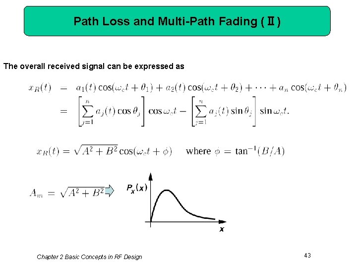
Path Loss and Multi-Path Fading (Ⅱ) The overall received signal can be expressed as Chapter 2 Basic Concepts in RF Design 43

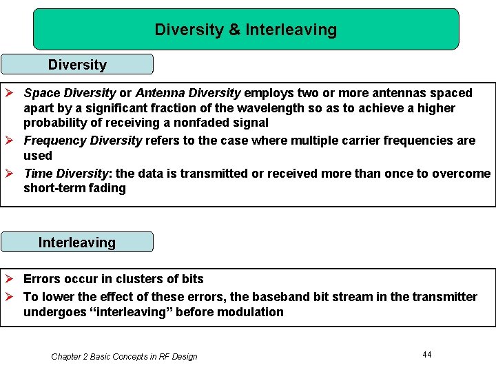
Diversity & Interleaving Diversity Ø Space Diversity or Antenna Diversity employs two or more antennas spaced apart by a significant fraction of the wavelength so as to achieve a higher probability of receiving a nonfaded signal Ø Frequency Diversity refers to the case where multiple carrier frequencies are used Ø Time Diversity: the data is transmitted or received more than once to overcome short-term fading Interleaving Ø Errors occur in clusters of bits Ø To lower the effect of these errors, the baseband bit stream in the transmitter undergoes “interleaving” before modulation Chapter 2 Basic Concepts in RF Design 44

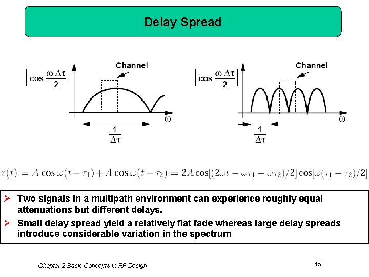
Delay Spread Ø Two signals in a multipath environment can experience roughly equal attenuations but different delays. Ø Small delay spread yield a relatively flat fade whereas large delay spreads introduce considerable variation in the spectrum Chapter 2 Basic Concepts in RF Design 45

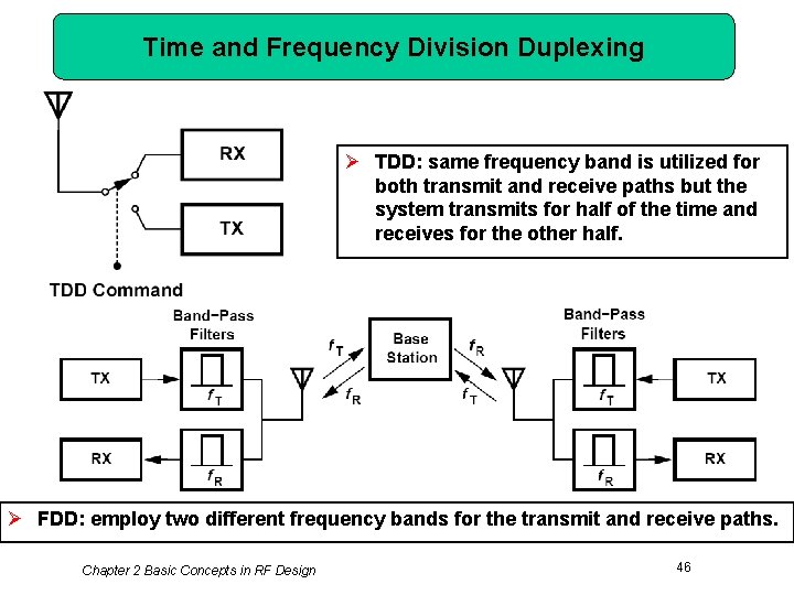
Time and Frequency Division Duplexing Ø TDD: same frequency band is utilized for both transmit and receive paths but the system transmits for half of the time and receives for the other half. Ø FDD: employ two different frequency bands for the transmit and receive paths. Chapter 2 Basic Concepts in RF Design 46

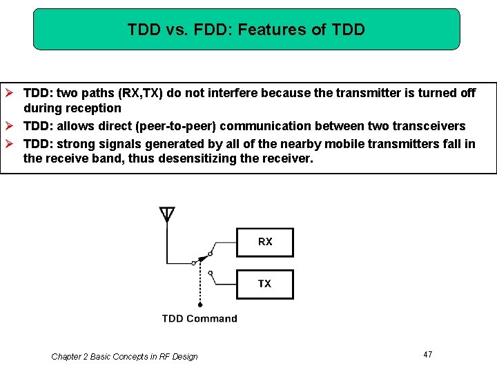
TDD vs. FDD: Features of TDD Ø TDD: two paths (RX, TX) do not interfere because the transmitter is turned off during reception Ø TDD: allows direct (peer-to-peer) communication between two transceivers Ø TDD: strong signals generated by all of the nearby mobile transmitters fall in the receive band, thus desensitizing the receiver. Chapter 2 Basic Concepts in RF Design 47

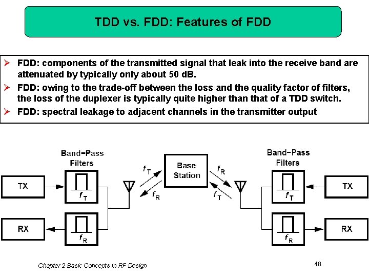
TDD vs. FDD: Features of FDD Ø FDD: components of the transmitted signal that leak into the receive band are attenuated by typically only about 50 d. B. Ø FDD: owing to the trade-off between the loss and the quality factor of filters, the loss of the duplexer is typically quite higher than that of a TDD switch. Ø FDD: spectral leakage to adjacent channels in the transmitter output Chapter 2 Basic Concepts in RF Design 48

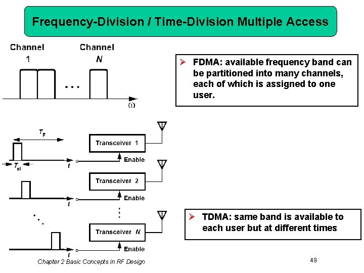
Frequency-Division / Time-Division Multiple Access Ø FDMA: available frequency band can be partitioned into many channels, each of which is assigned to one user. Ø TDMA: same band is available to each user but at different times Chapter 2 Basic Concepts in RF Design 49

TDMA Features: Compared with FDMA Ø TDMA: power amplifier can be turned off during the time of the frame out of assigned time slot Ø TDMA: digitized speech can be compressed in time by a large factor, smaller required bandwidth. Ø TDMA: even with FDD, TDMA bursts can e timed so the receive and transmit paths are never enabled simultaneously Ø TDMA: more complex due to A/D conversion, digital modulation, time slot and frame synchronization, etc. Chapter 2 Basic Concepts in RF Design 50

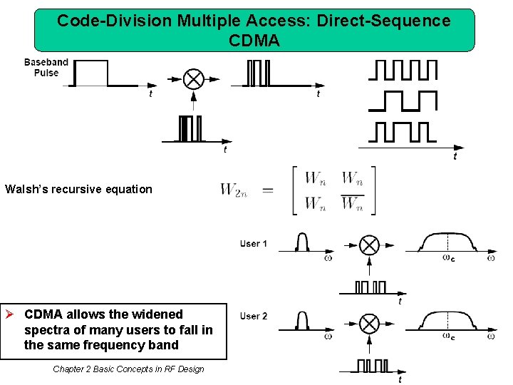
Code-Division Multiple Access: Direct-Sequence CDMA Walsh’s recursive equation Ø CDMA allows the widened spectra of many users to fall in the same frequency band Chapter 2 Basic Concepts in RF Design 51

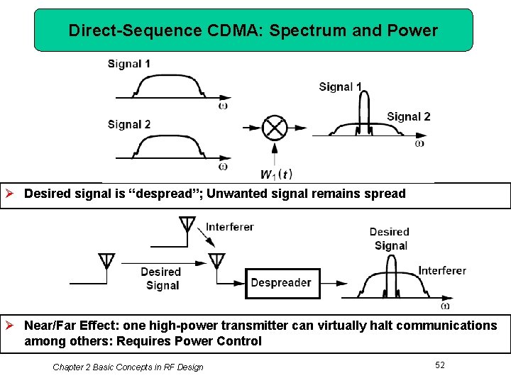
Direct-Sequence CDMA: Spectrum and Power Ø Desired signal is “despread”; Unwanted signal remains spread Ø Near/Far Effect: one high-power transmitter can virtually halt communications among others: Requires Power Control Chapter 2 Basic Concepts in RF Design 52

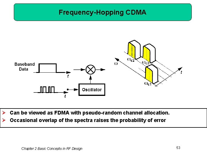
Frequency-Hopping CDMA Ø Can be viewed as FDMA with pseudo-random channel allocation. Ø Occasional overlap of the spectra raises the probability of error Chapter 2 Basic Concepts in RF Design 53

Wireless Standards: Common Specifications (Ⅰ) Ø 1. Frequency Bands and Channelization: Each standard performs communication in an allocated frequency band Ø 2. Data Rates: The standard specifies the data rates that must be supported Ø 3. Antenna Duplexing Method: Most cellular phone systems incorporate FDD and other standards employ TDD Ø 4. Type of Modulation: Each standard specifies the modulation scheme. Chapter 2 Basic Concepts in RF Design 54

Wireless Standards: Common Specifications (Ⅱ) Ø 5. TX output power: The standard specifies the power levels that the TX must produce Ø 6. TX EVM and Spectral Mask: The signal transmitted by the TX must satisfy several requirements like EVM and spectral mask Ø 7. RX Sensitivity: The standard specifies the acceptable receiver sensitivity, usually in terms of maximum BER Ø 8. RX Input Level Range: The standard specifies the desired signal range that the receiver must handle with acceptable noise or distortion Chapter 2 Basic Concepts in RF Design 55

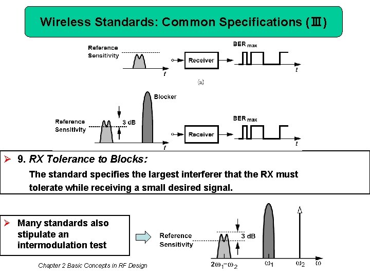
Wireless Standards: Common Specifications (Ⅲ) Ø 9. RX Tolerance to Blocks: The standard specifies the largest interferer that the RX must tolerate while receiving a small desired signal. Ø Many standards also stipulate an intermodulation test Chapter 2 Basic Concepts in RF Design 56

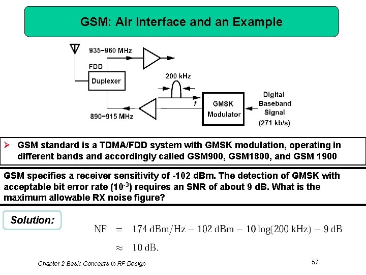
GSM: Air Interface and an Example Ø GSM standard is a TDMA/FDD system with GMSK modulation, operating in different bands and accordingly called GSM 900, GSM 1800, and GSM 1900 GSM specifies a receiver sensitivity of -102 d. Bm. The detection of GMSK with acceptable bit error rate (10 -3) requires an SNR of about 9 d. B. What is the maximum allowable RX noise figure? Solution: Chapter 2 Basic Concepts in RF Design 57

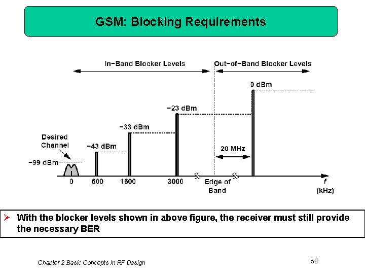
GSM: Blocking Requirements Ø With the blocker levels shown in above figure, the receiver must still provide the necessary BER Chapter 2 Basic Concepts in RF Design 58

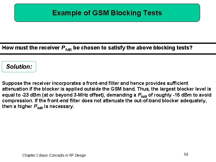
Example of GSM Blocking Tests How must the receiver P 1 d. B be chosen to satisfy the above blocking tests? Solution: Suppose the receiver incorporates a front-end filter and hence provides sufficient attenuation if the blocker is applied outside the GSM band. Thus, the largest blocker level is equal to -23 d. Bm (at or beyond 3 -MHz offset), demanding a P 1 d. B of roughly -15 d. Bm to avoid compression. If the front-end filter does not attenuate the out-of-band blocker adequately, then a higher P 1 d. B is necessary. Chapter 2 Basic Concepts in RF Design 59

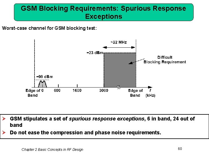
GSM Blocking Requirements: Spurious Response Exceptions Worst-case channel for GSM blocking test: Ø GSM stipulates a set of spurious response exceptions, 6 in band, 24 out of band Ø Do not ease the compression and phase noise requirements. Chapter 2 Basic Concepts in RF Design 60

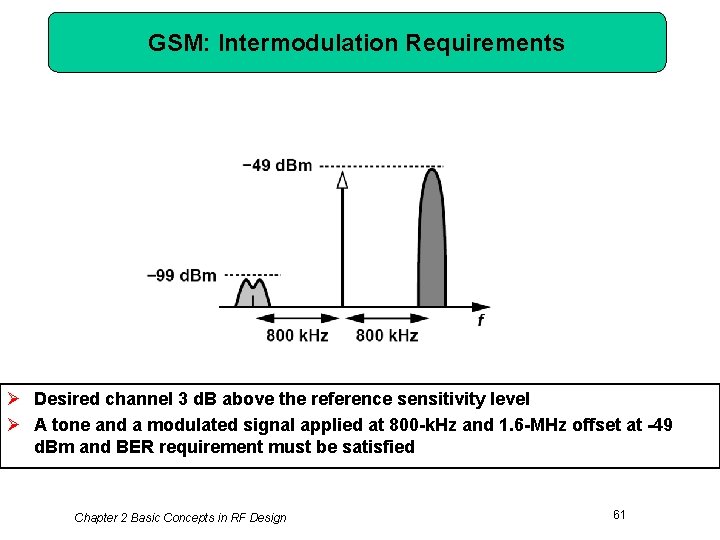
GSM: Intermodulation Requirements Ø Desired channel 3 d. B above the reference sensitivity level Ø A tone and a modulated signal applied at 800 -k. Hz and 1. 6 -MHz offset at -49 d. Bm and BER requirement must be satisfied Chapter 2 Basic Concepts in RF Design 61

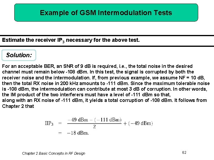
Example of GSM Intermodulation Tests Estimate the receiver IP 3 necessary for the above test. Solution: For an acceptable BER, an SNR of 9 d. B is required, i. e. , the total noise in the desired channel must remain below -108 d. Bm. In this test, the signal is corrupted by both the receiver noise and the intermodulation. If, from previous example, we assume NF = 10 d. B, then the total RX noise in 200 k. Hz amounts to -111 d. Bm. Since the maximum tolerable noise is -108 d. Bm, the intermodulation can contribute at most 3 d. B of corruption. In other words, the IM product of the two interferers must have a level of -111 d. Bm so that, along with an RX noise of -111 d. Bm, it yields a total corruption of -108 d. Bm. It follows from Chapter 2 that Chapter 2 Basic Concepts in RF Design 62

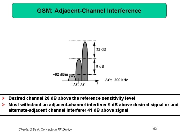
GSM: Adjacent-Channel Interference Ø Desired channel 20 d. B above the reference sensitivity level Ø Must withstand an adjacent-channel interferer 9 d. B above desired signal or and alternate-adjacent channel interferer 41 d. B above signal Chapter 2 Basic Concepts in RF Design 63

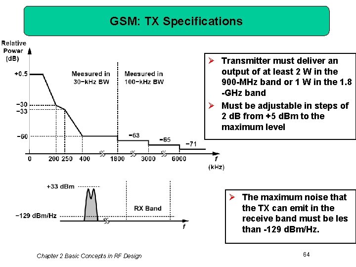
GSM: TX Specifications Ø Transmitter must deliver an output of at least 2 W in the 900 -MHz band or 1 W in the 1. 8 -GHz band Ø Must be adjustable in steps of 2 d. B from +5 d. Bm to the maximum level Ø The maximum noise that the TX can emit in the receive band must be les than -129 d. Bm/Hz. Chapter 2 Basic Concepts in RF Design 64

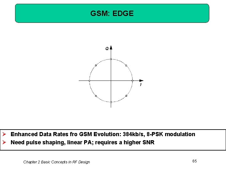
GSM: EDGE Ø Enhanced Data Rates fro GSM Evolution: 384 kb/s, 8 -PSK modulation Ø Need pulse shaping, linear PA; requires a higher SNR Chapter 2 Basic Concepts in RF Design 65

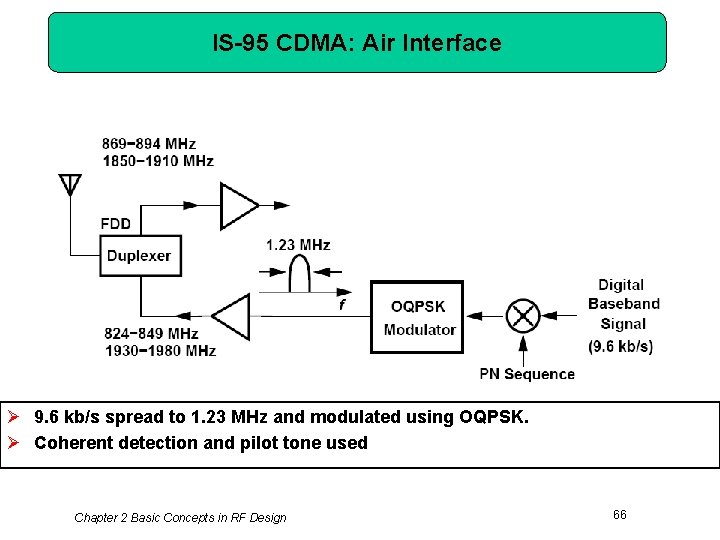
IS-95 CDMA: Air Interface Ø 9. 6 kb/s spread to 1. 23 MHz and modulated using OQPSK. Ø Coherent detection and pilot tone used Chapter 2 Basic Concepts in RF Design 66

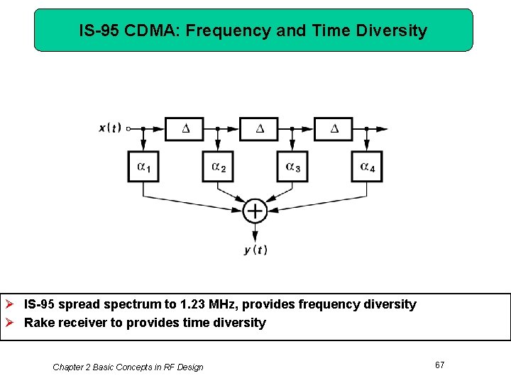
IS-95 CDMA: Frequency and Time Diversity Ø IS-95 spread spectrum to 1. 23 MHz, provides frequency diversity Ø Rake receiver to provides time diversity Chapter 2 Basic Concepts in RF Design 67

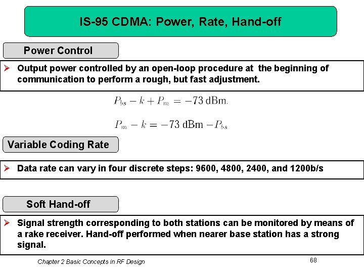
IS-95 CDMA: Power, Rate, Hand-off Power Control Ø Output power controlled by an open-loop procedure at the beginning of communication to perform a rough, but fast adjustment. Variable Coding Rate Ø Data rate can vary in four discrete steps: 9600, 4800, 2400, and 1200 b/s Soft Hand-off Ø Signal strength corresponding to both stations can be monitored by means of a rake receiver. Hand-off performed when nearer base station has a strong signal. Chapter 2 Basic Concepts in RF Design 68

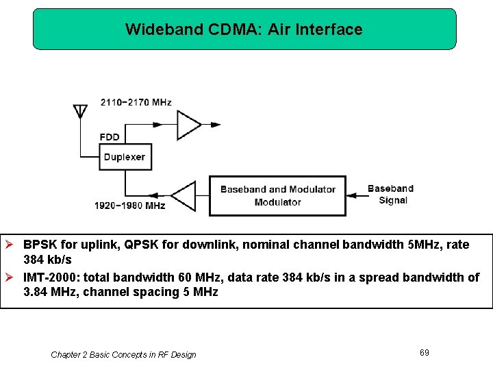
Wideband CDMA: Air Interface Ø BPSK for uplink, QPSK for downlink, nominal channel bandwidth 5 MHz, rate 384 kb/s Ø IMT-2000: total bandwidth 60 MHz, data rate 384 kb/s in a spread bandwidth of 3. 84 MHz, channel spacing 5 MHz Chapter 2 Basic Concepts in RF Design 69

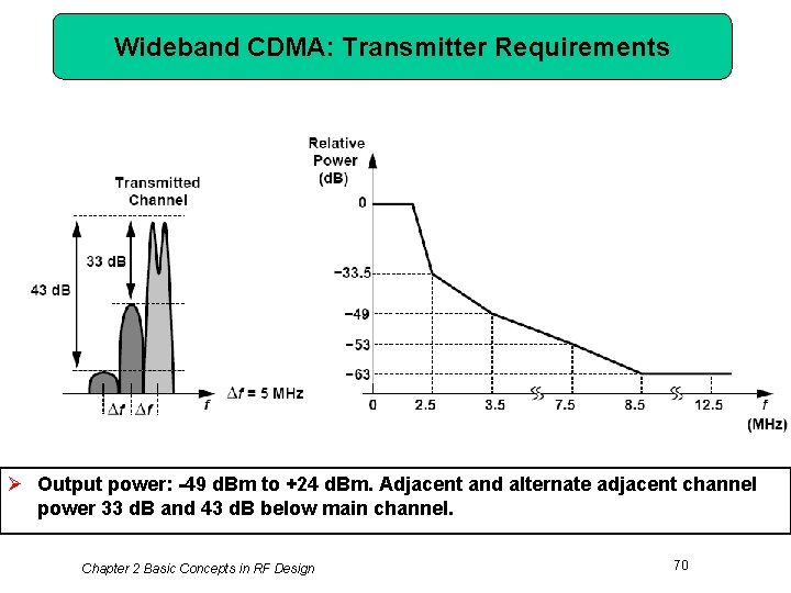
Wideband CDMA: Transmitter Requirements Ø Output power: -49 d. Bm to +24 d. Bm. Adjacent and alternate adjacent channel power 33 d. B and 43 d. B below main channel. Chapter 2 Basic Concepts in RF Design 70

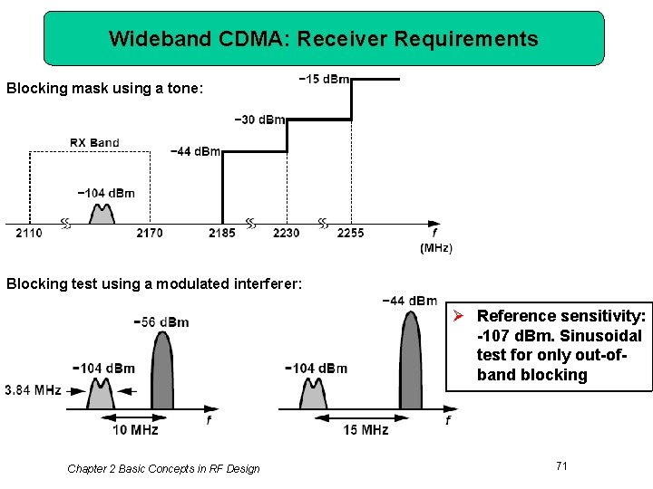
Wideband CDMA: Receiver Requirements Blocking mask using a tone: Blocking test using a modulated interferer: Ø Reference sensitivity: -107 d. Bm. Sinusoidal test for only out-ofband blocking Chapter 2 Basic Concepts in RF Design 71

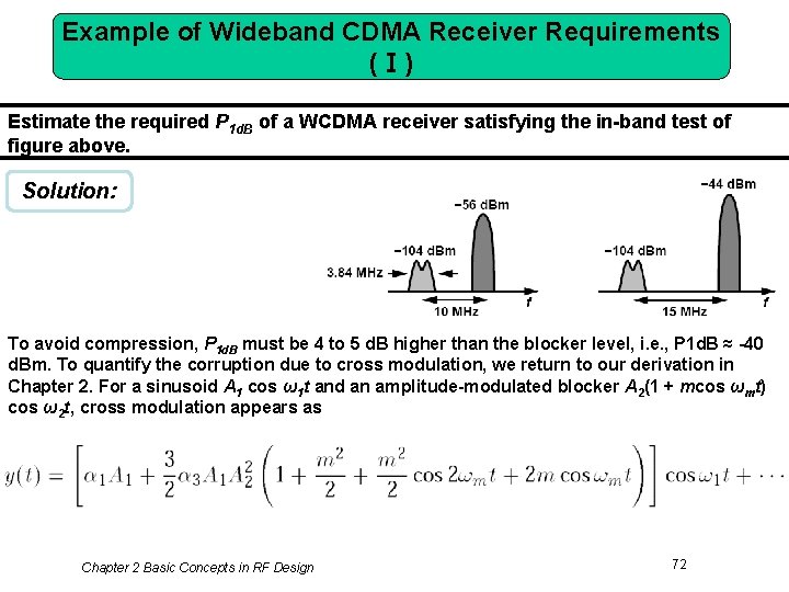
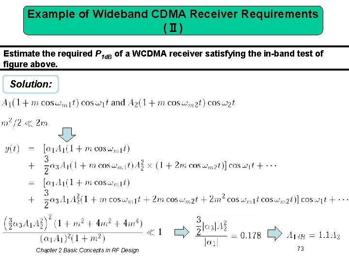
Example of Wideband CDMA Receiver Requirements (Ⅰ) Estimate the required P 1 d. B of a WCDMA receiver satisfying the in-band test of figure above. Solution: To avoid compression, P 1 d. B must be 4 to 5 d. B higher than the blocker level, i. e. , P 1 d. B ≈ -40 d. Bm. To quantify the corruption due to cross modulation, we return to our derivation in Chapter 2. For a sinusoid A 1 cos ω1 t and an amplitude-modulated blocker A 2(1 + mcos ωmt) cos ω2 t, cross modulation appears as Chapter 2 Basic Concepts in RF Design 72

Example of Wideband CDMA Receiver Requirements (Ⅱ) Estimate the required P 1 d. B of a WCDMA receiver satisfying the in-band test of figure above. Solution: Chapter 2 Basic Concepts in RF Design 73

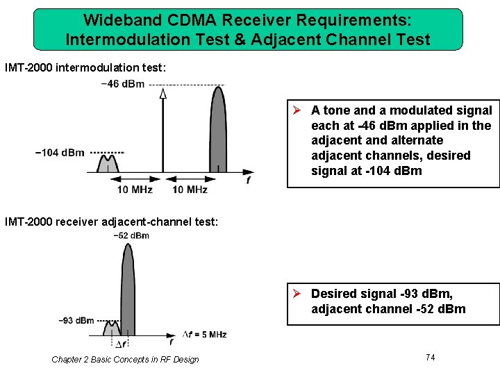
Wideband CDMA Receiver Requirements: Intermodulation Test & Adjacent Channel Test IMT-2000 intermodulation test: Ø A tone and a modulated signal each at -46 d. Bm applied in the adjacent and alternate adjacent channels, desired signal at -104 d. Bm IMT-2000 receiver adjacent-channel test: Ø Desired signal -93 d. Bm, adjacent channel -52 d. Bm Chapter 2 Basic Concepts in RF Design 74

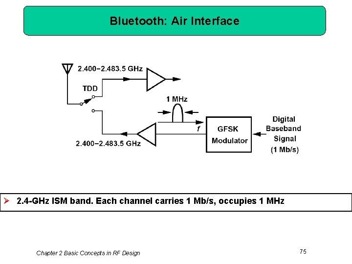
Bluetooth: Air Interface Ø 2. 4 -GHz ISM band. Each channel carries 1 Mb/s, occupies 1 MHz Chapter 2 Basic Concepts in RF Design 75

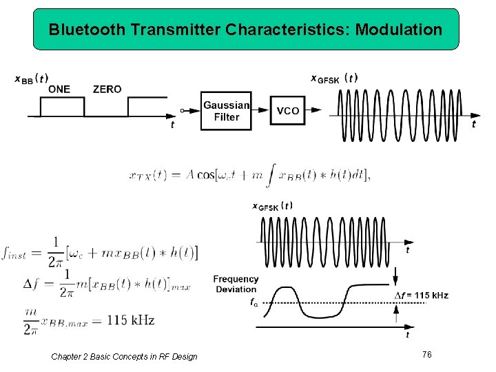
Bluetooth Transmitter Characteristics: Modulation Chapter 2 Basic Concepts in RF Design 76

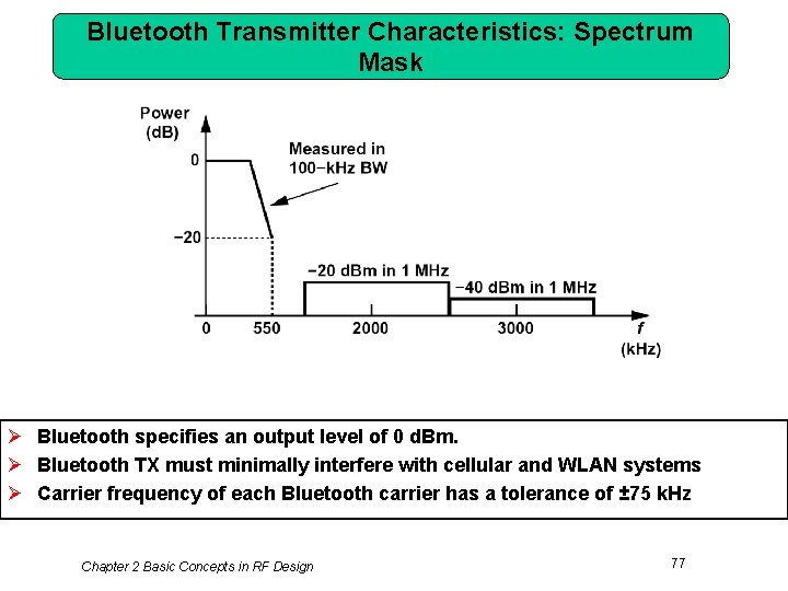
Bluetooth Transmitter Characteristics: Spectrum Mask Ø Bluetooth specifies an output level of 0 d. Bm. Ø Bluetooth TX must minimally interfere with cellular and WLAN systems Ø Carrier frequency of each Bluetooth carrier has a tolerance of ± 75 k. Hz Chapter 2 Basic Concepts in RF Design 77

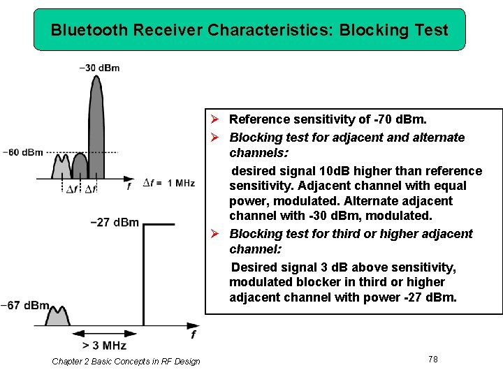
Bluetooth Receiver Characteristics: Blocking Test Ø Reference sensitivity of -70 d. Bm. Ø Blocking test for adjacent and alternate channels: desired signal 10 d. B higher than reference sensitivity. Adjacent channel with equal power, modulated. Alternate adjacent channel with -30 d. Bm, modulated. Ø Blocking test for third or higher adjacent channel: Desired signal 3 d. B above sensitivity, modulated blocker in third or higher adjacent channel with power -27 d. Bm. Chapter 2 Basic Concepts in RF Design 78

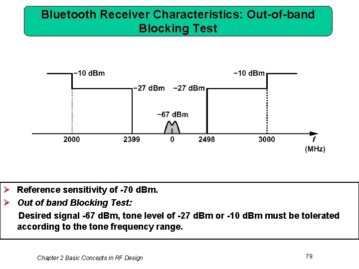
Bluetooth Receiver Characteristics: Out-of-band Blocking Test Ø Reference sensitivity of -70 d. Bm. Ø Out of band Blocking Test: Desired signal -67 d. Bm, tone level of -27 d. Bm or -10 d. Bm must be tolerated according to the tone frequency range. Chapter 2 Basic Concepts in RF Design 79

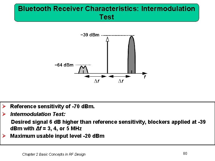
Bluetooth Receiver Characteristics: Intermodulation Test Ø Reference sensitivity of -70 d. Bm. Ø Intermodulation Test: Desired signal 6 d. B higher than reference sensitivity, blockers applied at -39 d. Bm with Δf = 3, 4, or 5 MHz Ø Maximum usable input level -20 d. Bm Chapter 2 Basic Concepts in RF Design 80

Example of Maximum Usable Input Specification Does the maximum usable input specification pose any design constraints? Solution: Yes, it does. Recall that the receiver must detect a signal as low as -60 d. Bm; i. e. , the receiver chain must provide enough gain before detection. Suppose this gain is about 60 d. B, yielding a signal level of around 0 d. Bm (632 m. Vpp) at the end of the chain. Now, if the received signal rises to -20 d. Bm, the RX output must reach +40 d. Bm (63. 2 Vpp), unless the chain becomes heavily nonlinear. The nonlinearity may appear benign as the signal has a constant envelope, but the heavy saturation of the stages may distort the baseband data. For this reason, the receiver must incorporate “automatic gain control” (AGC), reducing the gain of each stage as the input signal level increases (Chapter 13). Chapter 2 Basic Concepts in RF Design 81

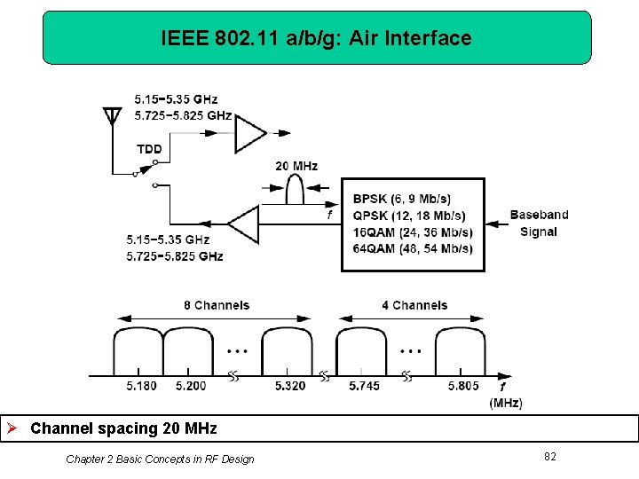
IEEE 802. 11 a/b/g: Air Interface Ø Channel spacing 20 MHz Chapter 2 Basic Concepts in RF Design 82

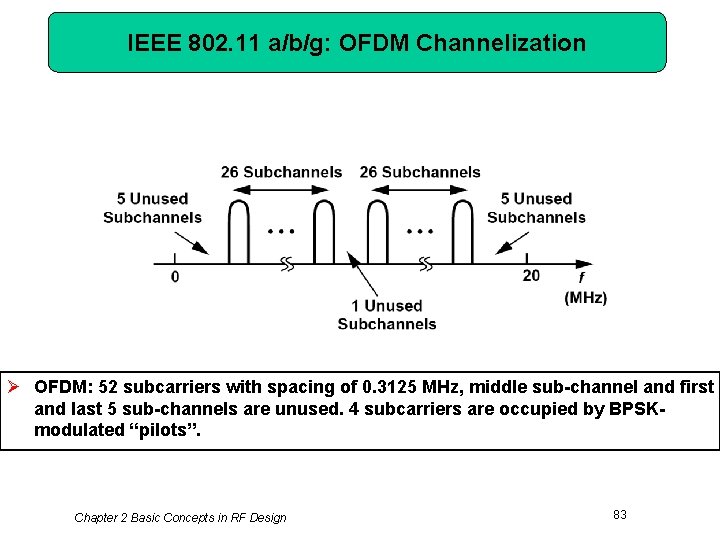
IEEE 802. 11 a/b/g: OFDM Channelization Ø OFDM: 52 subcarriers with spacing of 0. 3125 MHz, middle sub-channel and first and last 5 sub-channels are unused. 4 subcarriers are occupied by BPSKmodulated “pilots”. Chapter 2 Basic Concepts in RF Design 83

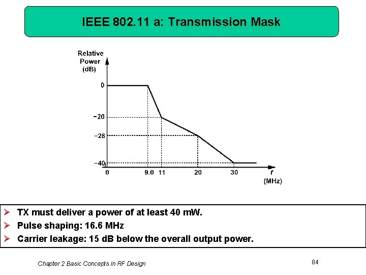
IEEE 802. 11 a: Transmission Mask Ø TX must deliver a power of at least 40 m. W. Ø Pulse shaping: 16. 6 MHz Ø Carrier leakage: 15 d. B below the overall output power. Chapter 2 Basic Concepts in RF Design 84

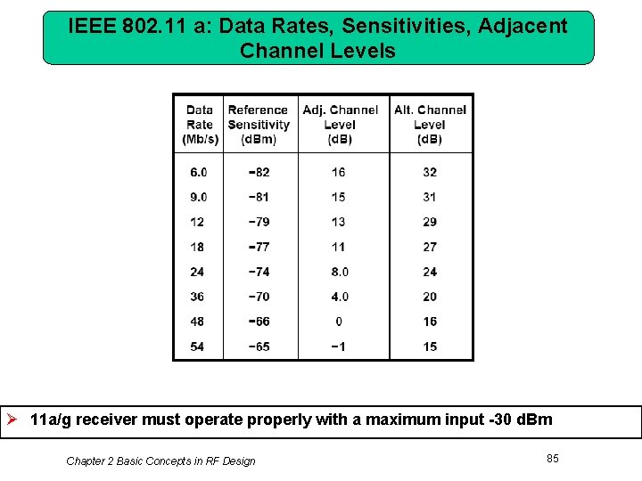
IEEE 802. 11 a: Data Rates, Sensitivities, Adjacent Channel Levels Ø 11 a/g receiver must operate properly with a maximum input -30 d. Bm Chapter 2 Basic Concepts in RF Design 85

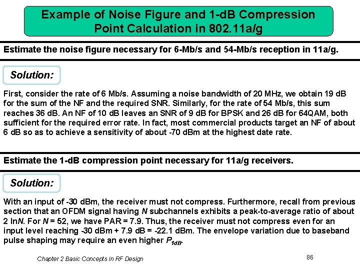
Example of Noise Figure and 1 -d. B Compression Point Calculation in 802. 11 a/g Estimate the noise figure necessary for 6 -Mb/s and 54 -Mb/s reception in 11 a/g. Solution: First, consider the rate of 6 Mb/s. Assuming a noise bandwidth of 20 MHz, we obtain 19 d. B for the sum of the NF and the required SNR. Similarly, for the rate of 54 Mb/s, this sum reaches 36 d. B. An NF of 10 d. B leaves an SNR of 9 d. B for BPSK and 26 d. B for 64 QAM, both sufficient for the required error rate. In fact, most commercial products target an NF of about 6 d. B so as to achieve a sensitivity of about -70 d. Bm at the highest date rate. Estimate the 1 -d. B compression point necessary for 11 a/g receivers. Solution: With an input of -30 d. Bm, the receiver must not compress. Furthermore, recall from previous section that an OFDM signal having N subchannels exhibits a peak-to-average ratio of about 2 ln. N. For N = 52, we have PAR = 7. 9. Thus, the receiver must not compress even for an input level reaching -30 d. Bm + 7. 9 d. B = -22. 1 d. Bm. The envelope variation due to baseband pulse shaping may require an even higher P 1 d. B. Chapter 2 Basic Concepts in RF Design 86

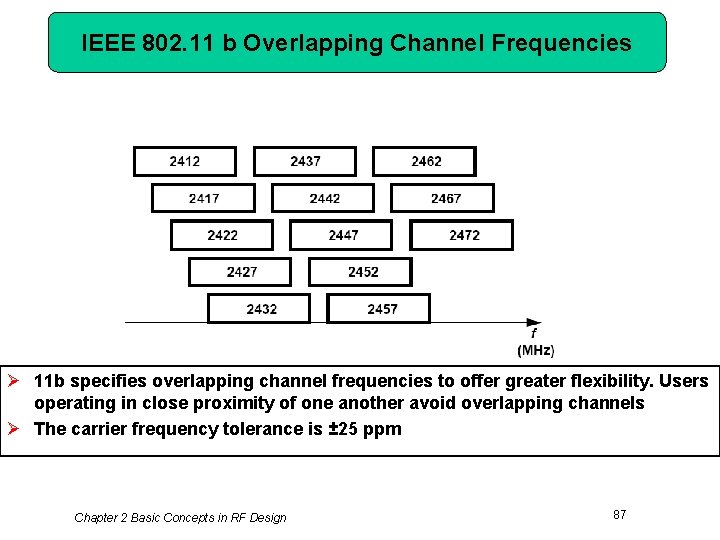
IEEE 802. 11 b Overlapping Channel Frequencies Ø 11 b specifies overlapping channel frequencies to offer greater flexibility. Users operating in close proximity of one another avoid overlapping channels Ø The carrier frequency tolerance is ± 25 ppm Chapter 2 Basic Concepts in RF Design 87

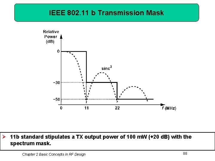
IEEE 802. 11 b Transmission Mask Ø 11 b standard stipulates a TX output power of 100 m. W (+20 d. B) with the spectrum mask. Chapter 2 Basic Concepts in RF Design 88

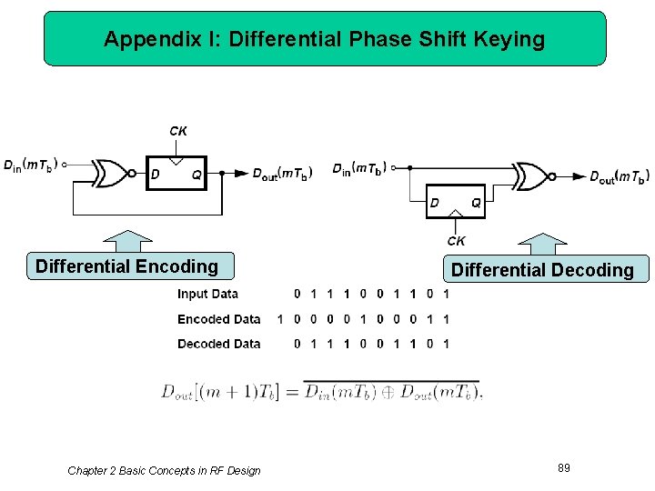
Appendix I: Differential Phase Shift Keying Differential Encoding Chapter 2 Basic Concepts in RF Design Differential Decoding 89

References (Ⅰ) Chapter 2 Basic Concepts in RF Design 90

References (Ⅱ) Chapter 2 Basic Concepts in RF Design 91