Chapter 3 Boolean Algebra We have seen how
Chapter 3: Boolean Algebra • We have seen how we can represent information in binary, now we will explore – Why we use binary – How to compute using binary – How to implement binary operations using Boolean algebra (such as binary addition) – How to implement Boolean algebra through digital circuits – How to store things using digital circuits • We will explore logic gates and use these to implement basic combinational circuits for adding, comparing, etc and sequential circuits for storage
Boolean Algebra • The basis for all digital circuits is Boolean algebra: – Boolean algebra is the algebra of binary values • or of 2 values – we refer to these values as 0 and 1 • although we could also refer to them as true and false – the basic Boolean algebra operations are • AND, OR, NOT, XOR, NAND and NOR (also COINCIDENCE) – you will have seen most of these in 260 and 262 but new ones are: • XOR – true if the two Boolean variables differ – true if x 1 = 1 and x 2 = 0 or x 1 = 0 and x 2 = 1, false otherwise • NAND and NOR are NOT of AND, and NOT of NOR respectively • COINCIDENCE is NOT of XOR – Each of these operations takes 2 inputs except NOT which takes 1 input – However, AND, OR, NAND and NOR can be generalized to accept any number of inputs
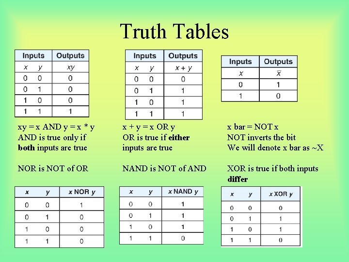
Truth Tables xy = x AND y = x * y AND is true only if both inputs are true x + y = x OR y OR is true if either inputs are true x bar = NOT x NOT inverts the bit We will denote x bar as ~X NOR is NOT of OR NAND is NOT of AND XOR is true if both inputs differ
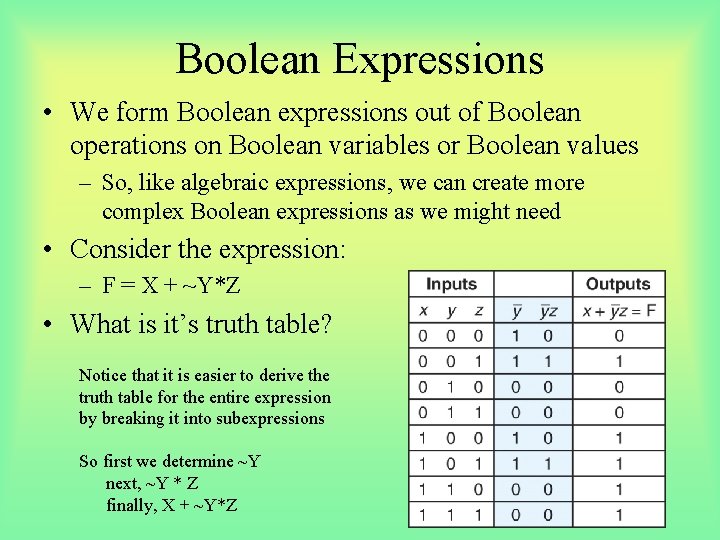
Boolean Expressions • We form Boolean expressions out of Boolean operations on Boolean variables or Boolean values – So, like algebraic expressions, we can create more complex Boolean expressions as we might need • Consider the expression: – F = X + ~Y*Z • What is it’s truth table? Notice that it is easier to derive the truth table for the entire expression by breaking it into subexpressions So first we determine ~Y next, ~Y * Z finally, X + ~Y*Z
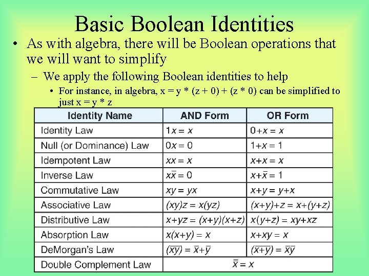
Basic Boolean Identities • As with algebra, there will be Boolean operations that we will want to simplify – We apply the following Boolean identities to help • For instance, in algebra, x = y * (z + 0) + (z * 0) can be simplified to just x = y * z
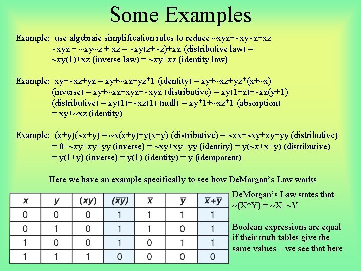
Some Examples Example: use algebraic simplification rules to reduce ~xyz+~xy~z+xz ~xyz + ~xy~z + xz = ~xy(z+~z)+xz (distributive law) = ~xy(1)+xz (inverse law) = ~xy+xz (identity law) Example: xy+~xz+yz = xy+~xz+yz*1 (identity) = xy+~xz+yz*(x+~x) (inverse) = xy+~xz+xyz+~xyz (distributive) = xy(1+z)+~xz(y+1) (distributive) = xy(1)+~xz(1) (null) = xy*1+~xz*1 (absorption) = xy+~xz (identity) Example: (x+y)(~x+y) = ~x(x+y)+y(x+y) (distributive) = ~xx+~xy+xy+yy (distributive) = 0+~xy+xy+yy (inverse) = ~xy+xy+yy (identity) = y(~x+x+y) (distributive) = y(1+y) (inverse) = y(1) (identity) = y (idempotent) Here we have an example specifically to see how De. Morgan’s Law works De. Morgan’s Law states that ~(X*Y) = ~X+~Y Boolean expressions are equal if their truth tables give the same values – we see that here
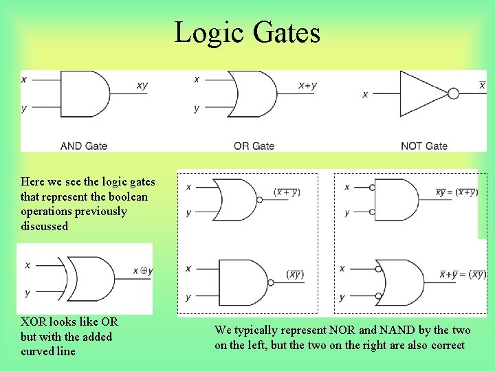
Logic Gates Here we see the logic gates that represent the boolean operations previously discussed XOR looks like OR but with the added curved line We typically represent NOR and NAND by the two on the left, but the two on the right are also correct
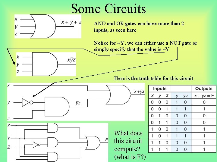
Some Circuits AND and OR gates can have more than 2 inputs, as seen here Notice for ~Y, we can either use a NOT gate or simply specify that the value is ~Y Here is the truth table for this circuit What does this circuit compute? (what is F? )
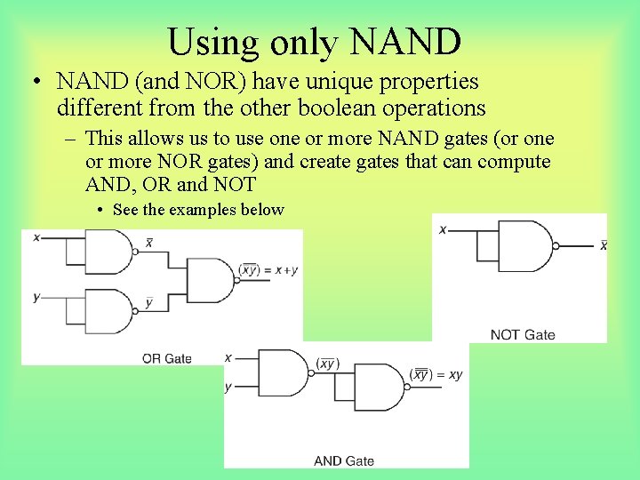
Using only NAND • NAND (and NOR) have unique properties different from the other boolean operations – This allows us to use one or more NAND gates (or one or more NOR gates) and create gates that can compute AND, OR and NOT • See the examples below
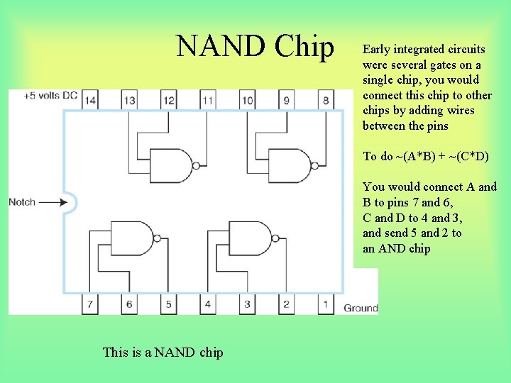
NAND Chip Early integrated circuits were several gates on a single chip, you would connect this chip to other chips by adding wires between the pins To do ~(A*B) + ~(C*D) You would connect A and B to pins 7 and 6, C and D to 4 and 3, and send 5 and 2 to an AND chip This is a NAND chip
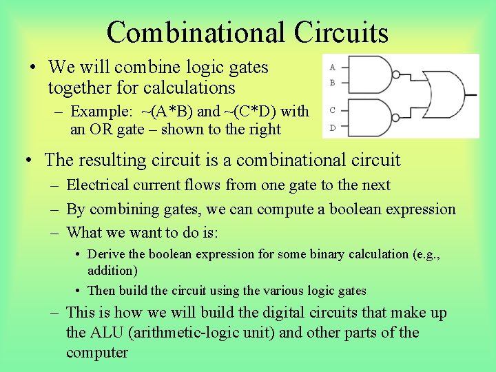
Combinational Circuits • We will combine logic gates together for calculations – Example: ~(A*B) and ~(C*D) with an OR gate – shown to the right • The resulting circuit is a combinational circuit – Electrical current flows from one gate to the next – By combining gates, we can compute a boolean expression – What we want to do is: • Derive the boolean expression for some binary calculation (e. g. , addition) • Then build the circuit using the various logic gates – This is how we will build the digital circuits that make up the ALU (arithmetic-logic unit) and other parts of the computer
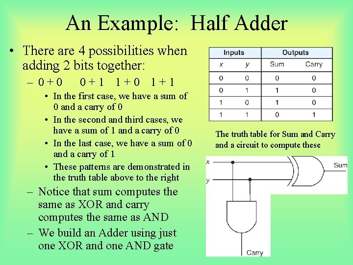
An Example: Half Adder • There are 4 possibilities when adding 2 bits together: – 0+0 0+1 1+0 1+1 • In the first case, we have a sum of 0 and a carry of 0 • In the second and third cases, we have a sum of 1 and a carry of 0 • In the last case, we have a sum of 0 and a carry of 1 • These patterns are demonstrated in the truth table above to the right – Notice that sum computes the same as XOR and carry computes the same as AND – We build an Adder using just one XOR and one AND gate The truth table for Sum and Carry and a circuit to compute these
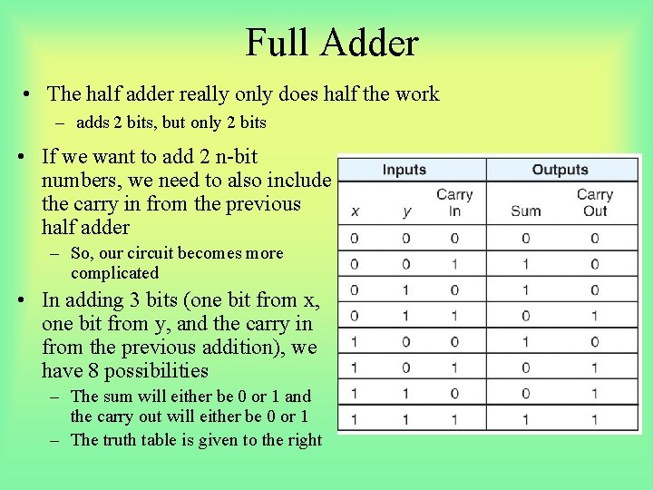
Full Adder • The half adder really only does half the work – adds 2 bits, but only 2 bits • If we want to add 2 n-bit numbers, we need to also include the carry in from the previous half adder – So, our circuit becomes more complicated • In adding 3 bits (one bit from x, one bit from y, and the carry in from the previous addition), we have 8 possibilities – The sum will either be 0 or 1 and the carry out will either be 0 or 1 – The truth table is given to the right
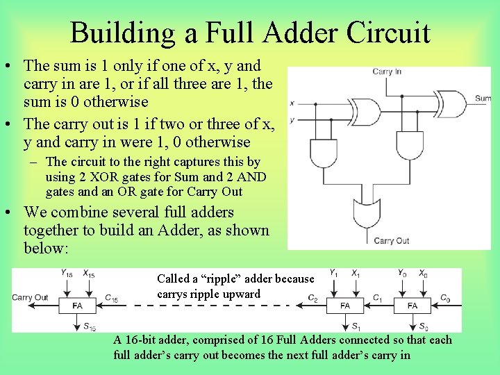
Building a Full Adder Circuit • The sum is 1 only if one of x, y and carry in are 1, or if all three are 1, the sum is 0 otherwise • The carry out is 1 if two or three of x, y and carry in were 1, 0 otherwise – The circuit to the right captures this by using 2 XOR gates for Sum and 2 AND gates and an OR gate for Carry Out • We combine several full adders together to build an Adder, as shown below: Called a “ripple” adder because carrys ripple upward A 16 -bit adder, comprised of 16 Full Adders connected so that each full adder’s carry out becomes the next full adder’s carry in
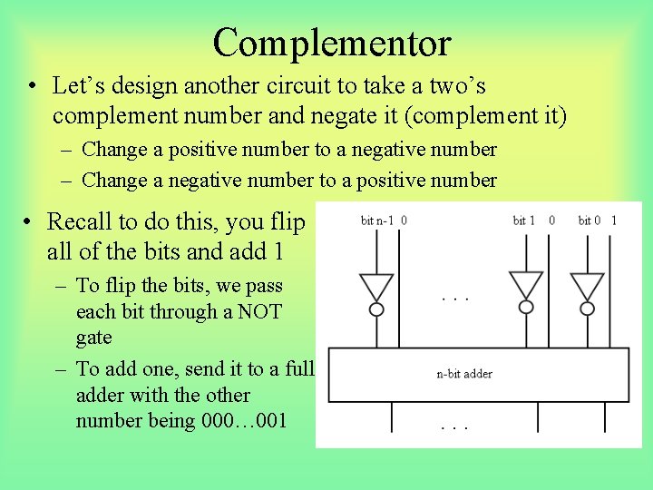
Complementor • Let’s design another circuit to take a two’s complement number and negate it (complement it) – Change a positive number to a negative number – Change a negative number to a positive number • Recall to do this, you flip all of the bits and add 1 – To flip the bits, we pass each bit through a NOT gate – To add one, send it to a full adder with the other number being 000… 001
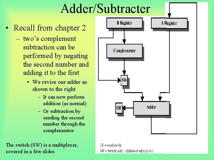
Adder/Subtracter • Recall from chapter 2 – two’s complement subtraction can be performed by negating the second number and adding it to the first • We revise our adder as shown to the right – It can now perform addition (as normal) – Or subtraction by sending the second number through the complementor The switch (SW) is a multiplexer, covered in a few slides
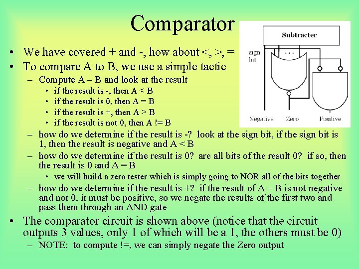
Comparator • We have covered + and -, how about <, >, = • To compare A to B, we use a simple tactic – Compute A – B and look at the result • • if the result is -, then A < B if the result is 0, then A = B if the result is +, then A > B if the result is not 0, then A != B – how do we determine if the result is -? look at the sign bit, if the sign bit is 1, then the result is negative and A < B – how do we determine if the result is 0? are all bits of the result 0? if so, then the result is 0 and A = B • we will build a zero tester which is simply going to NOR all of the bits together – how do we determine if the result is +? if the result of A – B is not negative and not 0, it must be positive, so we negate the results of the first two and pass them through an AND gate • The comparator circuit is shown above (notice that the circuit outputs 3 values, only 1 of which will be a 1, the others must be 0) – NOTE: to compute !=, we can simply negate the Zero output
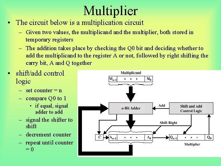
Multiplier • The circuit below is a multiplication circuit – Given two values, the multiplicand the multiplier, both stored in temporary registers – The addition takes place by checking the Q 0 bit and deciding whether to add the multiplicand to the register A or not, followed by right shifting the carry bit, A and Q together • shift/add control logic – set counter = n – compare Q 0 to 1 • if equal, signal adder to add – signal the shifter to shift – decrement counter – repeat until counter =0
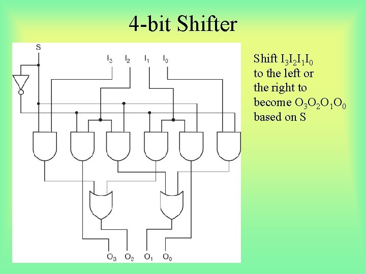
4 -bit Shifter Shift I 3 I 2 I 1 I 0 to the left or the right to become O 3 O 2 O 1 O 0 based on S
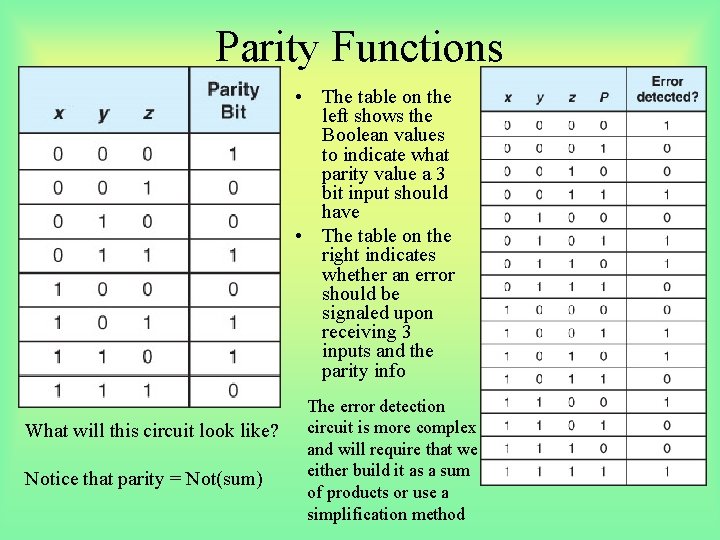
Parity Functions • The table on the left shows the Boolean values to indicate what parity value a 3 bit input should have • The table on the right indicates whether an error should be signaled upon receiving 3 inputs and the parity info What will this circuit look like? Notice that parity = Not(sum) The error detection circuit is more complex and will require that we either build it as a sum of products or use a simplification method
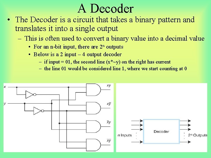
A Decoder • The Decoder is a circuit that takes a binary pattern and translates it into a single output – This is often used to convert a binary value into a decimal value • For an n-bit input, there are 2 n outputs • Below is a 2 input – 4 output decoder – if input = 01, the second line (x*~y) on the right has current – the line 01 would be considered line 1, where we start counting at 0
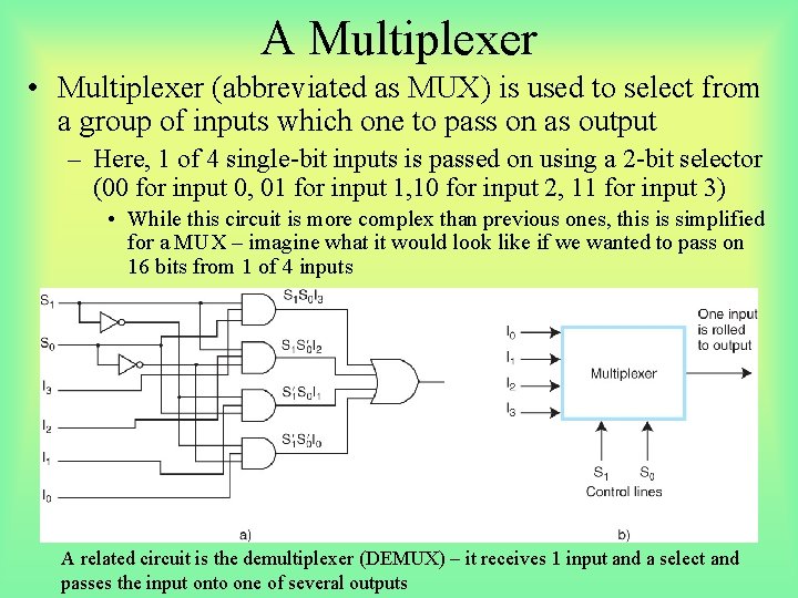
A Multiplexer • Multiplexer (abbreviated as MUX) is used to select from a group of inputs which one to pass on as output – Here, 1 of 4 single-bit inputs is passed on using a 2 -bit selector (00 for input 0, 01 for input 1, 10 for input 2, 11 for input 3) • While this circuit is more complex than previous ones, this is simplified for a MUX – imagine what it would look like if we wanted to pass on 16 bits from 1 of 4 inputs A related circuit is the demultiplexer (DEMUX) – it receives 1 input and a select and passes the input onto one of several outputs
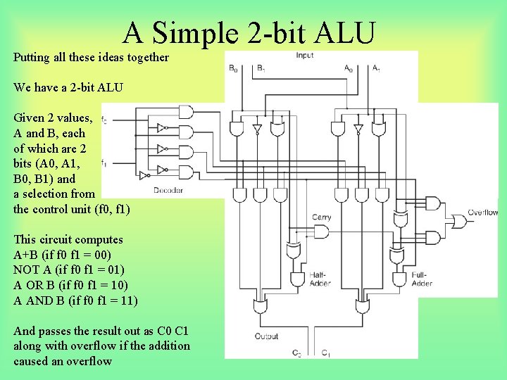
A Simple 2 -bit ALU Putting all these ideas together We have a 2 -bit ALU Given 2 values, A and B, each of which are 2 bits (A 0, A 1, B 0, B 1) and a selection from the control unit (f 0, f 1) This circuit computes A+B (if f 0 f 1 = 00) NOT A (if f 0 f 1 = 01) A OR B (if f 0 f 1 = 10) A AND B (if f 0 f 1 = 11) And passes the result out as C 0 C 1 along with overflow if the addition caused an overflow
Sequential Circuits • All of the previous circuits were combinational circuits – Current flowed in at one end and out the other – Combinational circuits cannot retain values – If we want to build a kind of memory, we need to use a sequential circuit • In a sequential circuit, current flows into the circuit and stays there • This is done by looping the output back into the input – Sequential circuits will be used to implement 1 -bit storage – We can then combine 1 -bit storage circuits into groups for nbit storage (registers, cache) • These circuits will be known as flip-flops because they can flip from one state (storing 1) to another (storing 0) or vice versa
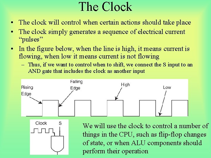
The Clock • The clock will control when certain actions should take place • The clock simply generates a sequence of electrical current “pulses” • In the figure below, when the line is high, it means current is flowing, when low it means current is not flowing – Thus, if we want to control when to shift, we connect the S input to an AND gate that includes the clock as another input We will use the clock to control a number of things in the CPU, such as flip-flop changes of state, or when ALU components should perform their operation
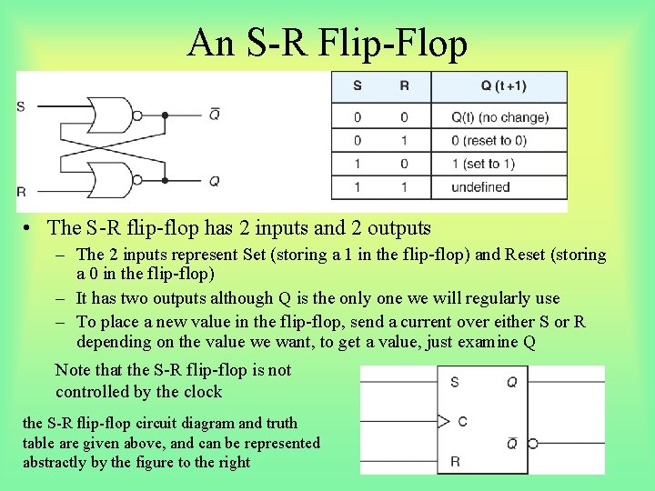
An S-R Flip-Flop • The S-R flip-flop has 2 inputs and 2 outputs – The 2 inputs represent Set (storing a 1 in the flip-flop) and Reset (storing a 0 in the flip-flop) – It has two outputs although Q is the only one we will regularly use – To place a new value in the flip-flop, send a current over either S or R depending on the value we want, to get a value, just examine Q Note that the S-R flip-flop is not controlled by the clock the S-R flip-flop circuit diagram and truth table are given above, and can be represented abstractly by the figure to the right
D and JK Flip-Flops
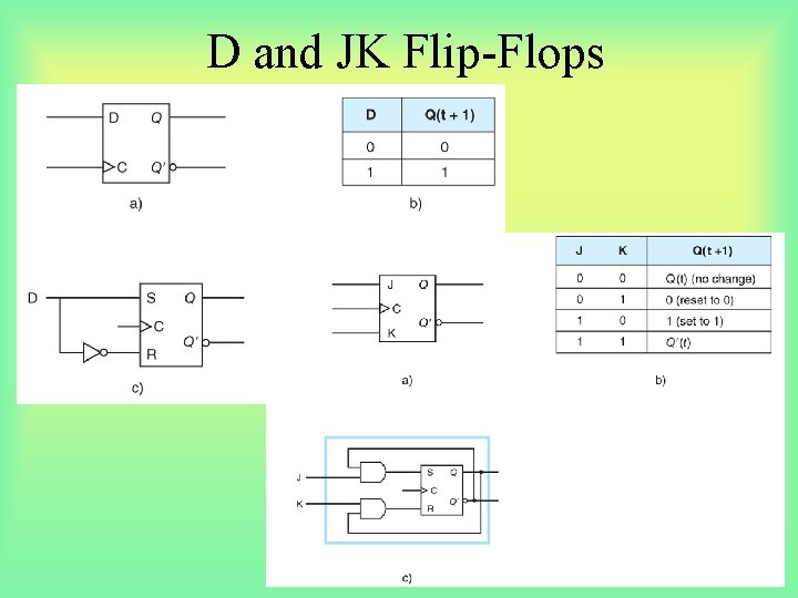
Registers • Since a single flip-flop stores a single bit, we combine n of them to create an n-bit register – However, the S-R flip-flop can be set or reset at any time, we instead want to use the system clock to determine when to change the value • So, we will use a D flip-flop instead – In the D flip-flop, there are 2 input lines, but they represent different things than the S-R flip-flop • One input is the clock – the flip-flop can only change when the clock pulses • The other input, labeled as D – is the input – if 0, then the flip-flop will store 0, – if 1 then the flip-flop will store 1 See figure 3. 22 for a D flip-flop Note: another flip-flop often used for storage is the J-K flip-flop, but since it is more complicated, we will skip it
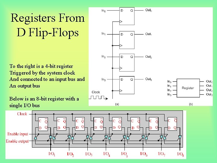
Registers From D Flip-Flops To the right is a 4 -bit register Triggered by the system clock And connected to an input bus and An output bus Below is an 8 -bit register with a single I/O bus
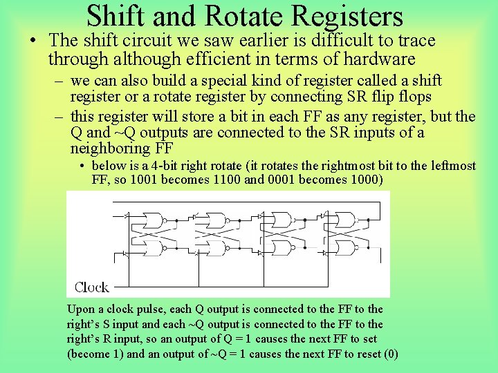
Shift and Rotate Registers • The shift circuit we saw earlier is difficult to trace through although efficient in terms of hardware – we can also build a special kind of register called a shift register or a rotate register by connecting SR flip flops – this register will store a bit in each FF as any register, but the Q and ~Q outputs are connected to the SR inputs of a neighboring FF • below is a 4 -bit right rotate (it rotates the rightmost bit to the leftmost FF, so 1001 becomes 1100 and 0001 becomes 1000) Upon a clock pulse, each Q output is connected to the FF to the right’s S input and each ~Q output is connected to the FF to the right’s R input, so an output of Q = 1 causes the next FF to set (become 1) and an output of ~Q = 1 causes the next FF to reset (0)
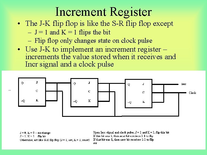
Increment Register • The J-K flip flop is like the S-R flip flop except – J = 1 and K = 1 flips the bit – Flip flop only changes state on clock pulse • Use J-K to implement an increment register – increments the value stored when it receives and Incr signal and a clock pulse
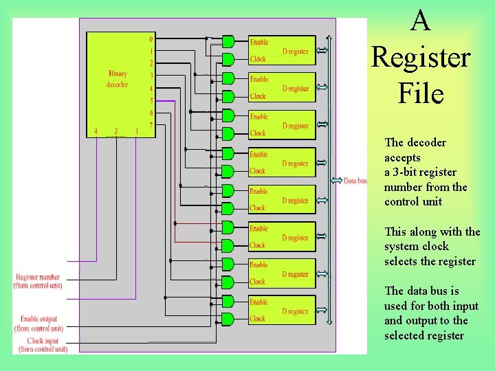
A Register File The decoder accepts a 3 -bit register number from the control unit This along with the system clock selects the register The data bus is used for both input and output to the selected register
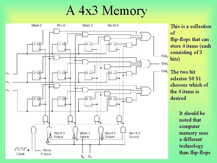
A 4 x 3 Memory This is a collection of flip-flops that can store 4 items (each consisting of 3 bits) The two bit selector S 0 S 1 chooses which of the 4 items is desired It should be noted that computer memory uses a different technology than flip-flops
- Slides: 33