Chapter 3 Basics Semiconductor Devices and Processing Hong
Chapter 3 Basics Semiconductor Devices and Processing Hong Xiao, Ph. D. www 2. austin. cc. tx. us/Hong. Xiao/Book. htm Hong Xiao, Ph. D. www 2. austin. cc. tx. us/Hong. Xiao/Boo k. htm 1
Objectives • Identify at least two semiconductor materials from the periodic table of elements • List n-type and p-type dopants • Describe a diode and a MOS transistor • List three kinds of chips made in the semiconductor industry • List at least four basic processes required for a chip manufacturing Hong Xiao, Ph. D. www 2. austin. cc. tx. us/Hong. Xiao/Boo k. htm 2
Topics • What is semiconductor • Basic semiconductor devices • Basics of IC processing Hong Xiao, Ph. D. www 2. austin. cc. tx. us/Hong. Xiao/Boo k. htm 3
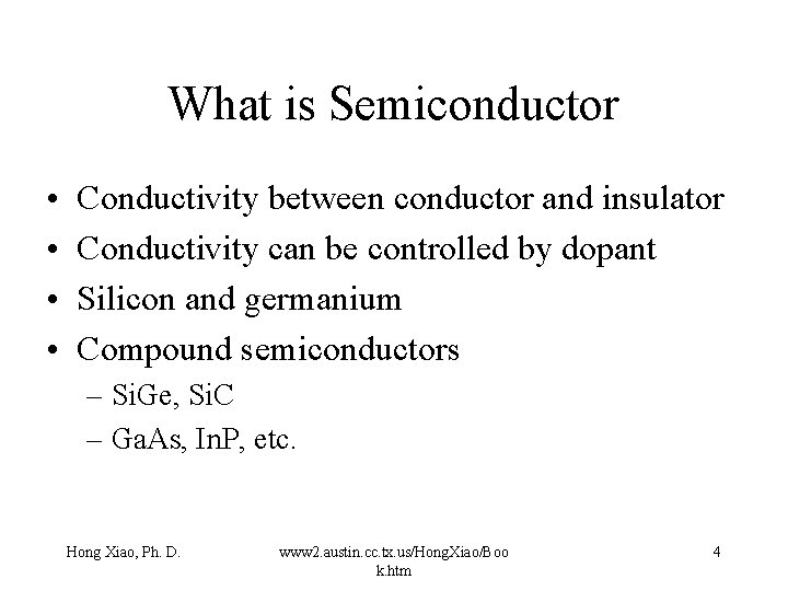
What is Semiconductor • • Conductivity between conductor and insulator Conductivity can be controlled by dopant Silicon and germanium Compound semiconductors – Si. Ge, Si. C – Ga. As, In. P, etc. Hong Xiao, Ph. D. www 2. austin. cc. tx. us/Hong. Xiao/Boo k. htm 4
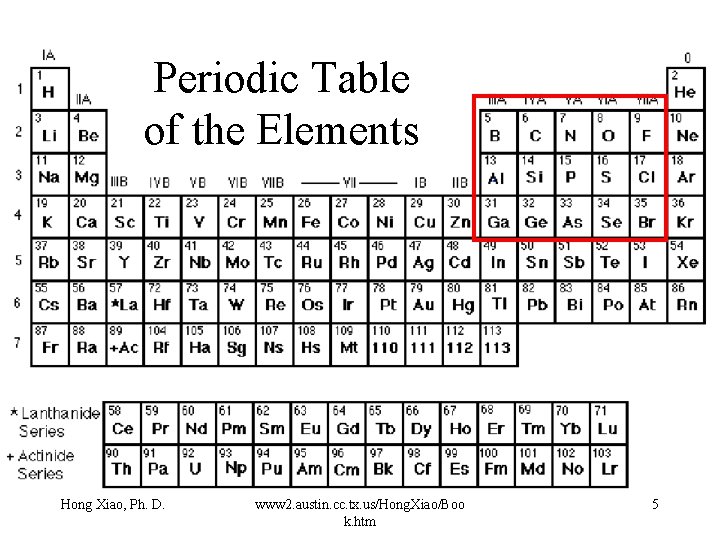
Periodic Table of the Elements Hong Xiao, Ph. D. www 2. austin. cc. tx. us/Hong. Xiao/Boo k. htm 5
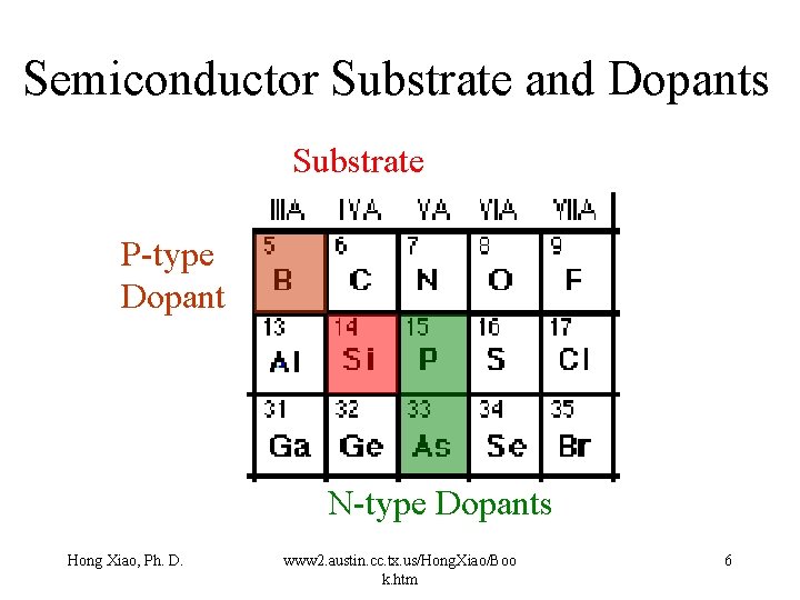
Semiconductor Substrate and Dopants Substrate P-type Dopant N-type Dopants Hong Xiao, Ph. D. www 2. austin. cc. tx. us/Hong. Xiao/Boo k. htm 6
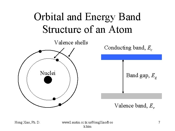
Orbital and Energy Band Structure of an Atom Valence shells Conducting band, Ec Nuclei Band gap, Eg Valence band, Ev Hong Xiao, Ph. D. www 2. austin. cc. tx. us/Hong. Xiao/Boo k. htm 7
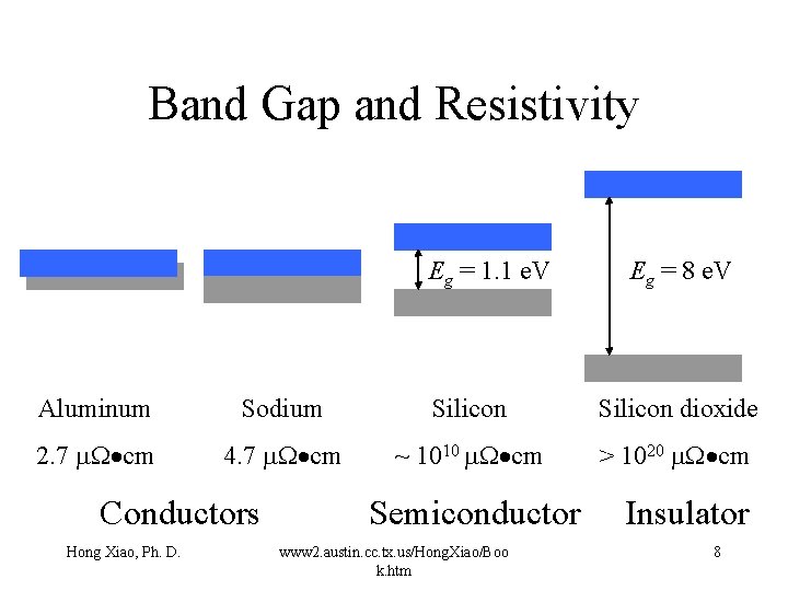
Band Gap and Resistivity Eg = 1. 1 e. V Eg = 8 e. V Aluminum Sodium Silicon dioxide 2. 7 m. W cm 4. 7 m. W cm ~ 1010 m. W cm > 1020 m. W cm Conductors Hong Xiao, Ph. D. Semiconductor www 2. austin. cc. tx. us/Hong. Xiao/Boo k. htm Insulator 8
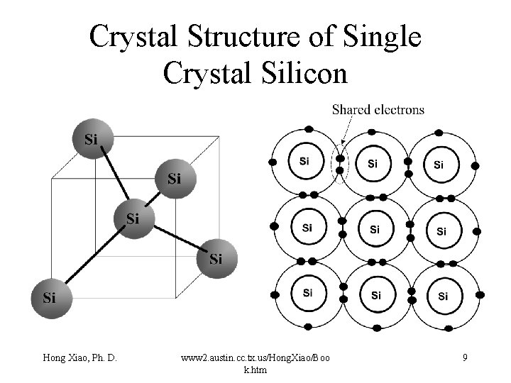
Crystal Structure of Single Crystal Silicon Hong Xiao, Ph. D. www 2. austin. cc. tx. us/Hong. Xiao/Boo k. htm 9
Why Silicon • Abundant, inexpensive • Thermal stability • Silicon dioxide is a strong dielectric and relatively easy to form • Silicon dioxide can be used as diffusion doping mask Hong Xiao, Ph. D. www 2. austin. cc. tx. us/Hong. Xiao/Boo k. htm 10
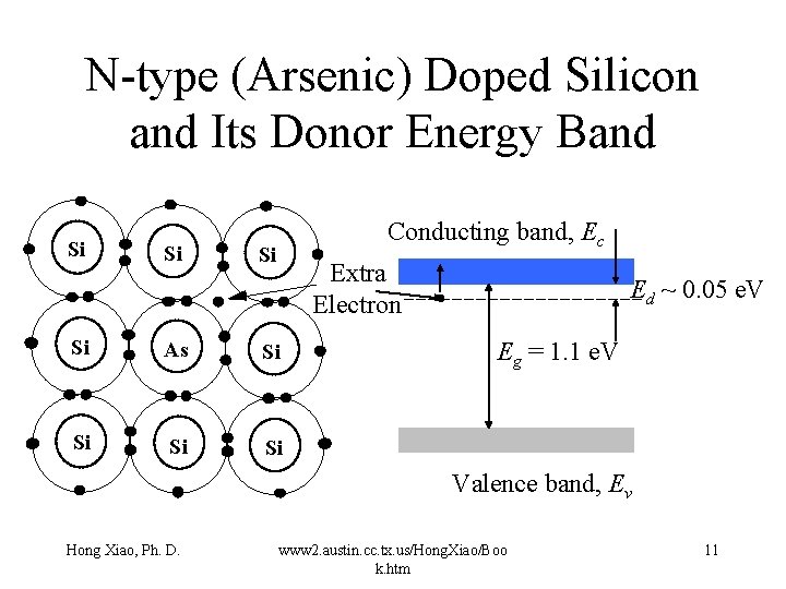
N-type (Arsenic) Doped Silicon and Its Donor Energy Band Si Si Si As Si Si Conducting band, Ec Si Extra Electron Si - Ed ~ 0. 05 e. V Eg = 1. 1 e. V Si Valence band, Ev Hong Xiao, Ph. D. www 2. austin. cc. tx. us/Hong. Xiao/Boo k. htm 11
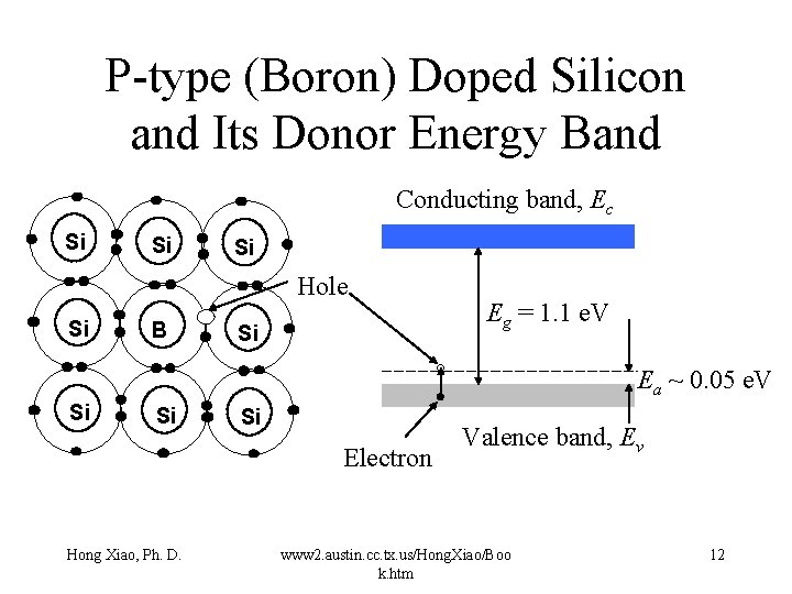
P-type (Boron) Doped Silicon and Its Donor Energy Band Conducting band, Ec Si Si Si Hole Si B Si Eg = 1. 1 e. V Ea ~ 0. 05 e. V Si Si - Si Electron Hong Xiao, Ph. D. Valence band, Ev www 2. austin. cc. tx. us/Hong. Xiao/Boo k. htm 12
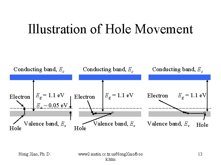
Illustration of Hole Movement Conducting band, Ec Electron Eg = 1. 1 e. V Ea ~ 0. 05 e. V Hole Valence band, Ev Hong Xiao, Ph. D. Conducting band, Ec Electron Hole Eg = 1. 1 e. V Valence band, Ev www 2. austin. cc. tx. us/Hong. Xiao/Boo k. htm Conducting band, Ec Electron Eg = 1. 1 e. V Valence band, Ev Hole 13
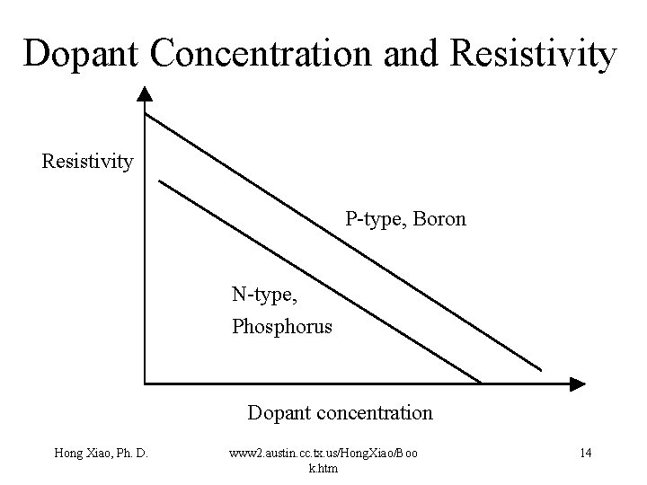
Dopant Concentration and Resistivity P-type, Boron N-type, Phosphorus Dopant concentration Hong Xiao, Ph. D. www 2. austin. cc. tx. us/Hong. Xiao/Boo k. htm 14
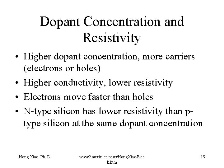
Dopant Concentration and Resistivity • Higher dopant concentration, more carriers (electrons or holes) • Higher conductivity, lower resistivity • Electrons move faster than holes • N-type silicon has lower resistivity than ptype silicon at the same dopant concentration Hong Xiao, Ph. D. www 2. austin. cc. tx. us/Hong. Xiao/Boo k. htm 15
Basic Devices • • • Hong Xiao, Ph. D. Resistor Capacitor Diode Bipolar Transistor MOS Transistor www 2. austin. cc. tx. us/Hong. Xiao/Boo k. htm 16
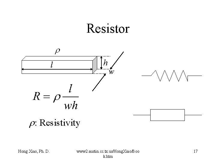
Resistor r h l w r: Resistivity Hong Xiao, Ph. D. www 2. austin. cc. tx. us/Hong. Xiao/Boo k. htm 17
Resistor • Resistors are made by doped silicon or polysilicon on an IC chip • Resistance is determined by length, line width, height, and dopant concentration Hong Xiao, Ph. D. www 2. austin. cc. tx. us/Hong. Xiao/Boo k. htm 18
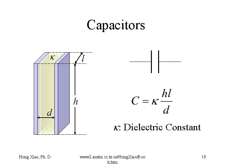
Capacitors k l h d k: Dielectric Constant Hong Xiao, Ph. D. www 2. austin. cc. tx. us/Hong. Xiao/Boo k. htm 19
Capacitors • Charge storage device • Memory Devices, esp. DRAM • Challenge: reduce capacitor size while keeping the capacitance • High-k dielectric materials Hong Xiao, Ph. D. www 2. austin. cc. tx. us/Hong. Xiao/Boo k. htm 20
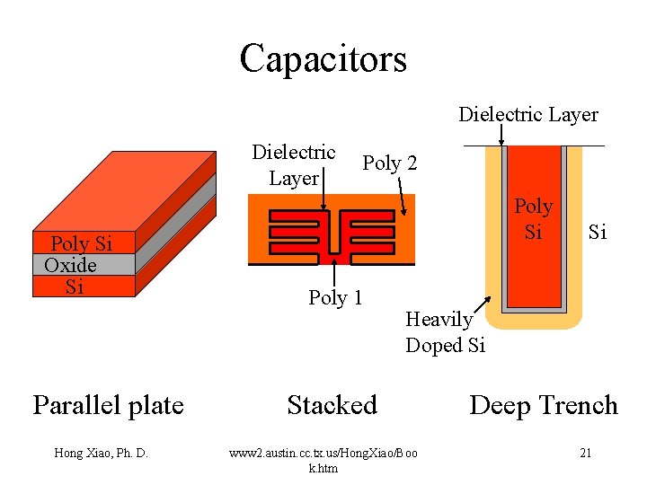
Capacitors Dielectric Layer Poly Si Oxide Si Parallel plate Hong Xiao, Ph. D. Poly 2 Poly Si Poly 1 Si Heavily Doped Si Stacked www 2. austin. cc. tx. us/Hong. Xiao/Boo k. htm Deep Trench 21
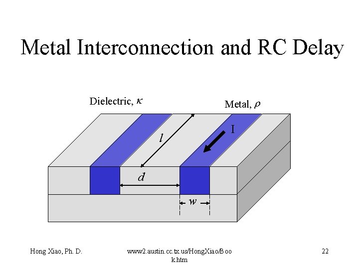
Metal Interconnection and RC Delay Dielectric, k Metal, r I l d w Hong Xiao, Ph. D. www 2. austin. cc. tx. us/Hong. Xiao/Boo k. htm 22
Diode • P-N Junction • Allows electric current go through only when it is positively biased. Hong Xiao, Ph. D. www 2. austin. cc. tx. us/Hong. Xiao/Boo k. htm 23

Diode Hong Xiao, Ph. D. www 2. austin. cc. tx. us/Hong. Xiao/Boo k. htm 24
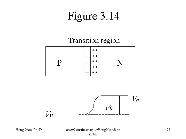
Figure 3. 14 Transition region P Vp Hong Xiao, Ph. D. ------ ++ ++ ++ N V 0 www 2. austin. cc. tx. us/Hong. Xiao/Boo k. htm Vn 25

Intrinsic Potential • For silicon V 0 ~ 0. 7 V Hong Xiao, Ph. D. www 2. austin. cc. tx. us/Hong. Xiao/Boo k. htm 26
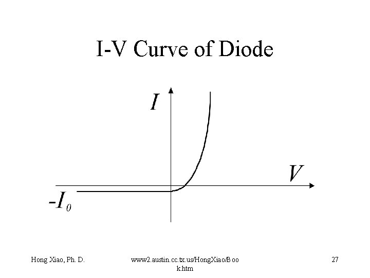
I-V Curve of Diode Hong Xiao, Ph. D. www 2. austin. cc. tx. us/Hong. Xiao/Boo k. htm 27
Bipolar Transistor • • • Hong Xiao, Ph. D. PNP or NPN Switch Amplifier Analog circuit Fast, high power device www 2. austin. cc. tx. us/Hong. Xiao/Boo k. htm 28
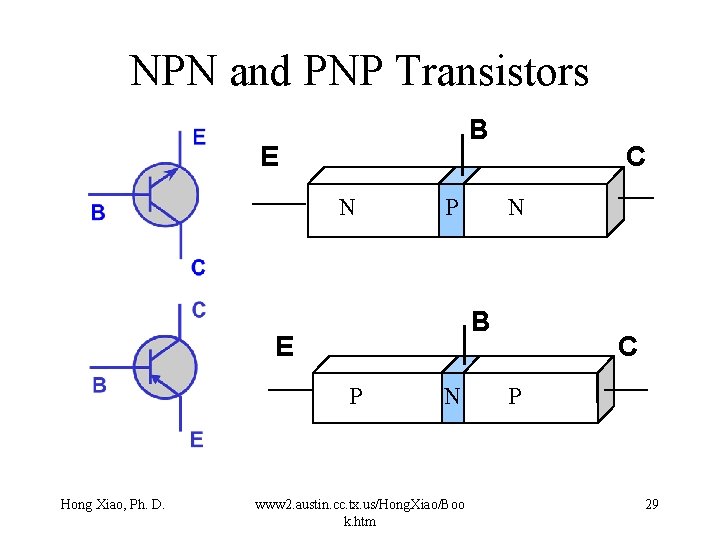
NPN and PNP Transistors B E N P N B E P Hong Xiao, Ph. D. C N www 2. austin. cc. tx. us/Hong. Xiao/Boo k. htm C P 29
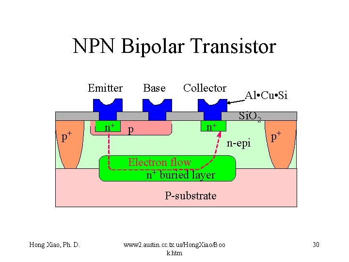
NPN Bipolar Transistor Emitter p+ n+ Base p Collector n+ Al • Cu • Si Si. O 2 n-epi p+ Electron flow n+ buried layer P-substrate Hong Xiao, Ph. D. www 2. austin. cc. tx. us/Hong. Xiao/Boo k. htm 30
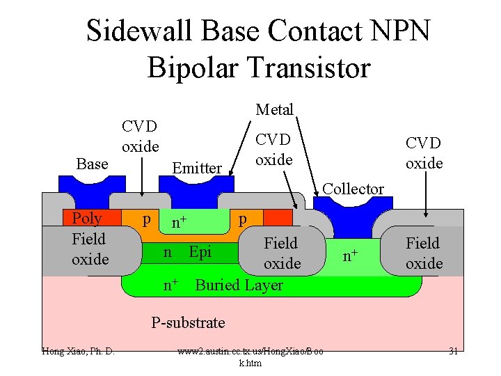
Sidewall Base Contact NPN Bipolar Transistor Base Metal CVD oxide Emitter CVD oxide Collector Poly Field oxide p p n+ n Field oxide Buried Layer Epi n+ n+ Field oxide P-substrate Hong Xiao, Ph. D. www 2. austin. cc. tx. us/Hong. Xiao/Boo k. htm 31
MOS Transistor • Metal-oxide-semiconductor • Also called MOSFET (MOS Field Effect Transistor) • Simple, symmetric structure • Switch, good for digital, logic circuit • Most commonly used devices in the semiconductor industry Hong Xiao, Ph. D. www 2. austin. cc. tx. us/Hong. Xiao/Boo k. htm 32
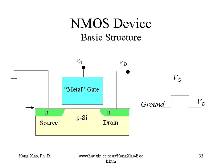
NMOS Device Basic Structure VG VD VG “Metal” Gate Ground n+ Source Hong Xiao, Ph. D. p-Si VD n+ Drain www 2. austin. cc. tx. us/Hong. Xiao/Boo k. htm 33
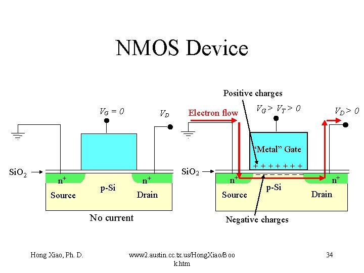
NMOS Device Positive charges VG = 0 VD Electron flow VG > V T > 0 VD > 0 “Metal” Gate Si. O 2 n+ Source n+ p-Si Drain No current Hong Xiao, Ph. D. Si. O 2 n+ Source +++++++ ------p-Si n+ Drain Negative charges www 2. austin. cc. tx. us/Hong. Xiao/Boo k. htm 34
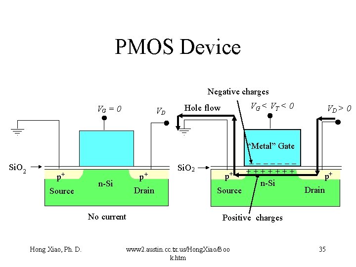
PMOS Device Negative charges VG = 0 VD VG < V T < 0 Hole flow VD > 0 “Metal” Gate Si. O 2 p+ Source p+ n-Si Drain No current Hong Xiao, Ph. D. Si. O 2 p+ Source ------+++++++ n-Si p+ Drain Positive charges www 2. austin. cc. tx. us/Hong. Xiao/Boo k. htm 35
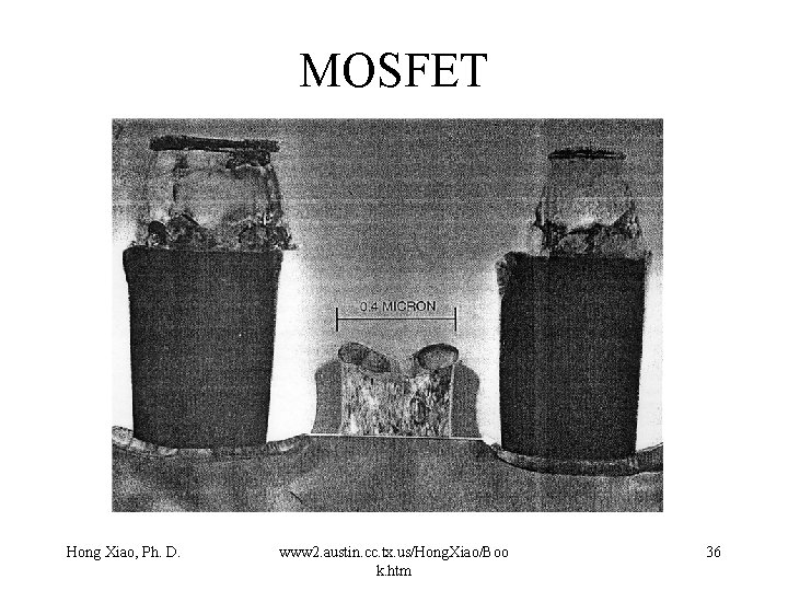
MOSFET Hong Xiao, Ph. D. www 2. austin. cc. tx. us/Hong. Xiao/Boo k. htm 36
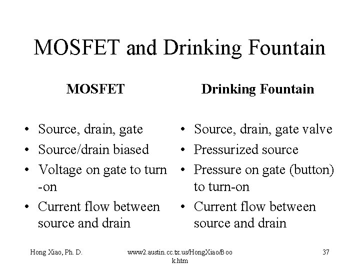
MOSFET and Drinking Fountain MOSFET Drinking Fountain • Source, drain, gate • Source/drain biased • Voltage on gate to turn -on • Current flow between source and drain • Source, drain, gate valve • Pressurized source • Pressure on gate (button) to turn-on • Current flow between source and drain Hong Xiao, Ph. D. www 2. austin. cc. tx. us/Hong. Xiao/Boo k. htm 37
Basic Circuits • • • Hong Xiao, Ph. D. Bipolar PMOS NMOS CMOS Bi. CMOS www 2. austin. cc. tx. us/Hong. Xiao/Boo k. htm 38
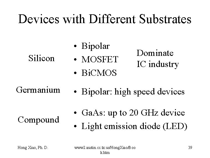
Devices with Different Substrates Silicon • Bipolar • MOSFET • Bi. CMOS Dominate IC industry Germanium • Bipolar: high speed devices Compound • Ga. As: up to 20 GHz device • Light emission diode (LED) Hong Xiao, Ph. D. www 2. austin. cc. tx. us/Hong. Xiao/Boo k. htm 39
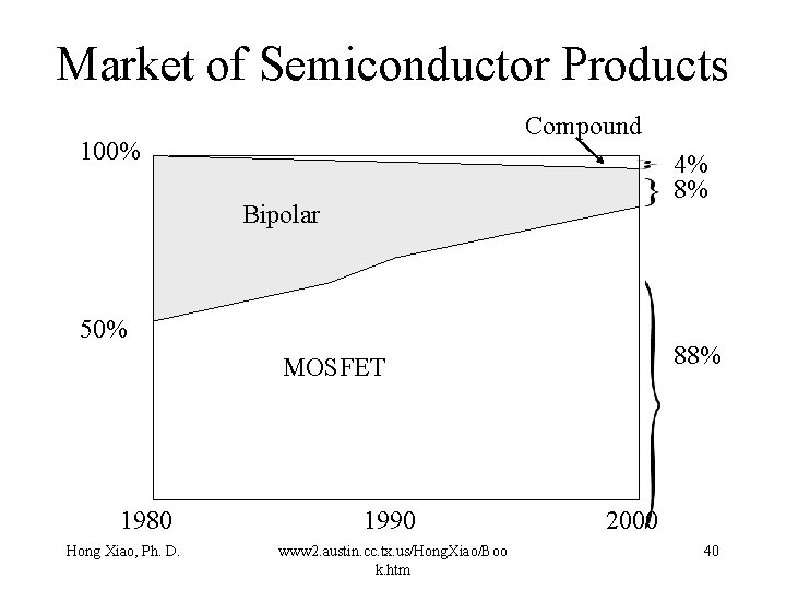
Market of Semiconductor Products Compound 100% 4% 8% Bipolar 50% 88% MOSFET 1980 Hong Xiao, Ph. D. 1990 www 2. austin. cc. tx. us/Hong. Xiao/Boo k. htm 2000 40
Bipolar IC • • Earliest IC chip 1961, four bipolar transistors, $150. 00 Market share reducing rapidly Still used for analog systems and power devices • TV, VCR, Cellar phone, etc. Hong Xiao, Ph. D. www 2. austin. cc. tx. us/Hong. Xiao/Boo k. htm 41
PMOS • First MOS field effect transistor, 1960 • Used for digital logic devices in the 1960 s • Replaced by NMOS after the mid-1970 s Hong Xiao, Ph. D. www 2. austin. cc. tx. us/Hong. Xiao/Boo k. htm 42
NMOS • Faster than PMOS • Used for digital logic devices in 1970 s and 1980 s • Electronic watches and hand-hold calculators • Replaced by CMOS after the 1980 s Hong Xiao, Ph. D. www 2. austin. cc. tx. us/Hong. Xiao/Boo k. htm 43
CMOS • Most commonly used circuit in IC chip since 1980 s • Low power consumption • High temperature stability • High noise immunity • Symmetric design Hong Xiao, Ph. D. www 2. austin. cc. tx. us/Hong. Xiao/Boo k. htm 44

CMOS Inverter Vdd PMOS V in Vout NMOS Vss Hong Xiao, Ph. D. www 2. austin. cc. tx. us/Hong. Xiao/Boo k. htm 45
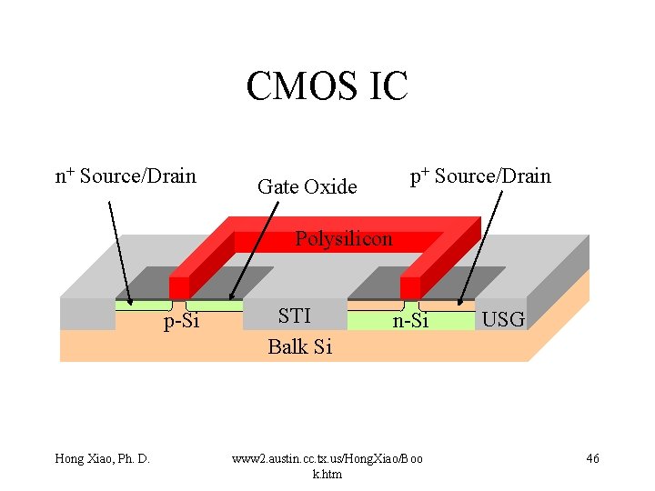
CMOS IC n+ Source/Drain p+ Source/Drain Gate Oxide Polysilicon p-Si Hong Xiao, Ph. D. STI Balk Si n-Si www 2. austin. cc. tx. us/Hong. Xiao/Boo k. htm USG 46
Bi. CMOS • • Combination of CMOS and bipolar circuits Mainly in 1990 s CMOS as logic circuit Bipolar for input/output Faster than CMOS Higher power consumption Likely will have problem when power supply voltage dropping below one volt Hong Xiao, Ph. D. www 2. austin. cc. tx. us/Hong. Xiao/Boo k. htm 47
IC Chips • Memory • Microprocessor • Application specific IC (ASIC) Hong Xiao, Ph. D. www 2. austin. cc. tx. us/Hong. Xiao/Boo k. htm 48
Memory Chips • Devices store data in the form of electric charge • Volatile memory – Dynamic random access memory (DRAM) – S random access memory (SRAM) • Non-volatile memory – Erasable programmable read only memory (EPROM) – FLASH Hong Xiao, Ph. D. www 2. austin. cc. tx. us/Hong. Xiao/Boo k. htm 49
DRAM • Major component of computer and other electronic instruments for data storage • Main driving force of IC processing development • One transistor, one capacitor Hong Xiao, Ph. D. www 2. austin. cc. tx. us/Hong. Xiao/Boo k. htm 50
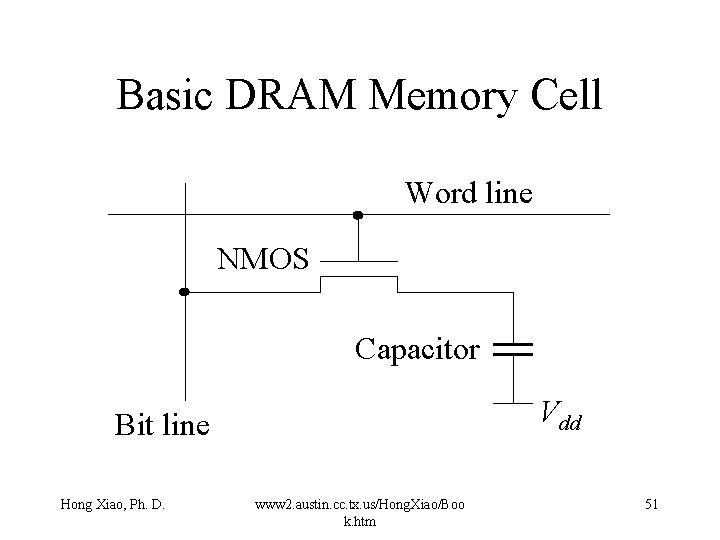
Basic DRAM Memory Cell Word line NMOS Capacitor Vdd Bit line Hong Xiao, Ph. D. www 2. austin. cc. tx. us/Hong. Xiao/Boo k. htm 51
SRAM • Fast memory application such as computer cache memory to store commonly used instructions • Unit memory cell consists of six transistors • Much faster than DRAM • More complicated processing, more expensive Hong Xiao, Ph. D. www 2. austin. cc. tx. us/Hong. Xiao/Boo k. htm 52
EPROM • Non-volatile memory • Keeping data ever without power supply • Computer bios memory which keeps boot up instructions • Floating gate • UV light memory erase Hong Xiao, Ph. D. www 2. austin. cc. tx. us/Hong. Xiao/Boo k. htm 53
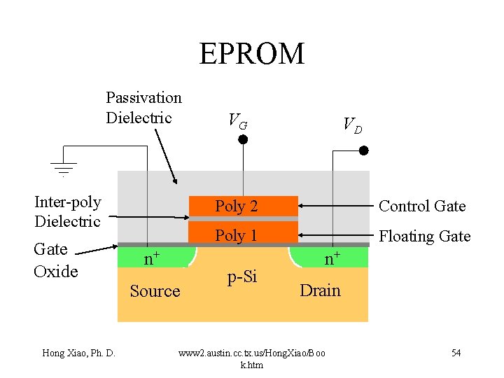
EPROM Passivation Dielectric Inter-poly Dielectric Gate Oxide Hong Xiao, Ph. D. n+ Source VG VD Poly 2 Control Gate Poly 1 Floating Gate p-Si n+ Drain www 2. austin. cc. tx. us/Hong. Xiao/Boo k. htm 54
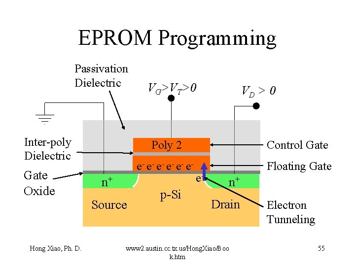
EPROM Programming Passivation Dielectric Inter-poly Dielectric Gate Oxide Hong Xiao, Ph. D. n+ Source VG>VT>0 VD > 0 Poly 2 Control Gate e- e- e- Floating Gate p-Si e- n+ Drain www 2. austin. cc. tx. us/Hong. Xiao/Boo k. htm Electron Tunneling 55
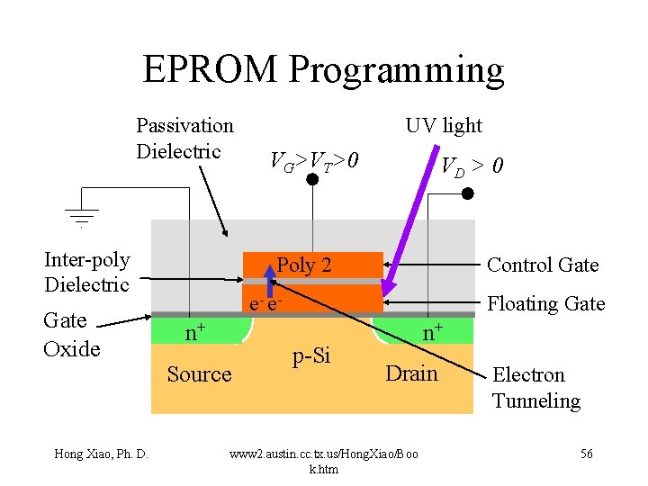
EPROM Programming Passivation Dielectric Inter-poly Dielectric Gate Oxide Hong Xiao, Ph. D. UV light VG>VT>0 VD > 0 Poly 2 Control Gate e- e- n+ Source Floating Gate p-Si n+ Drain www 2. austin. cc. tx. us/Hong. Xiao/Boo k. htm Electron Tunneling 56
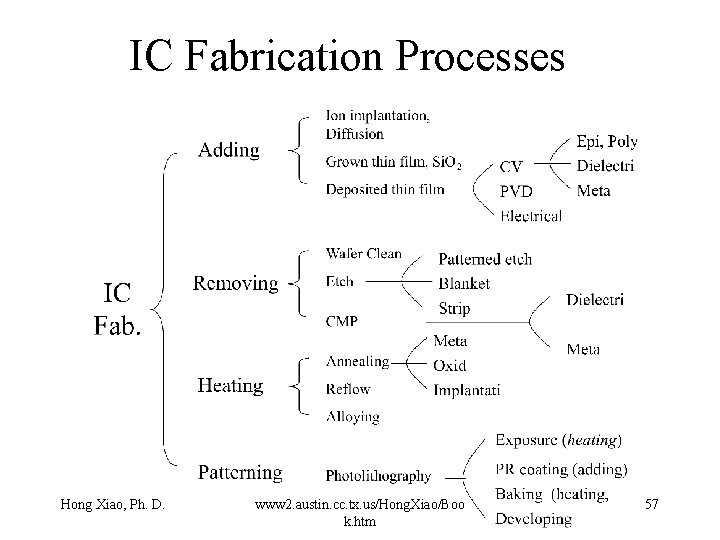
IC Fabrication Processes Hong Xiao, Ph. D. www 2. austin. cc. tx. us/Hong. Xiao/Boo k. htm 57
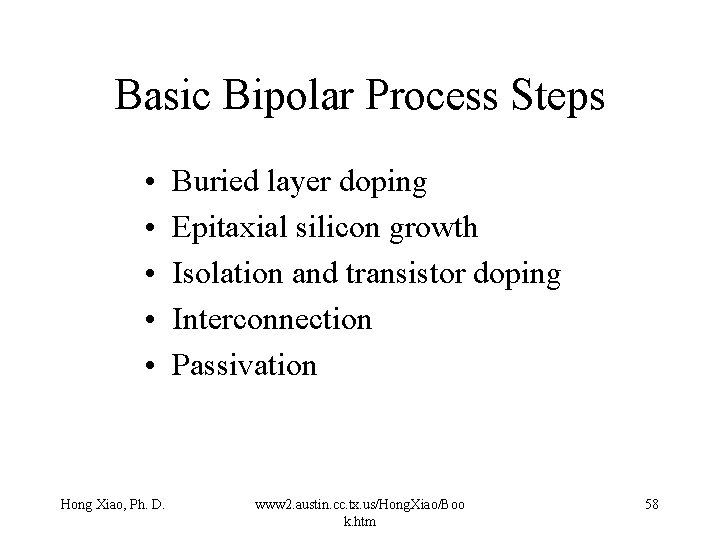
Basic Bipolar Process Steps • • • Hong Xiao, Ph. D. Buried layer doping Epitaxial silicon growth Isolation and transistor doping Interconnection Passivation www 2. austin. cc. tx. us/Hong. Xiao/Boo k. htm 58
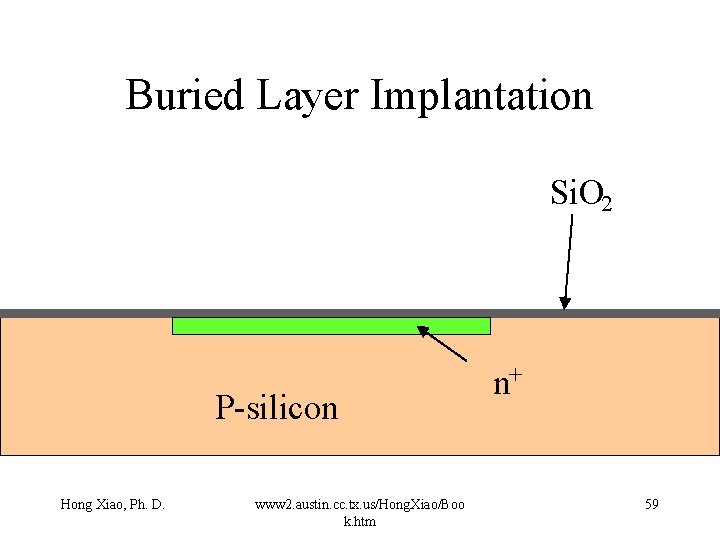
Buried Layer Implantation Si. O 2 P-silicon Hong Xiao, Ph. D. www 2. austin. cc. tx. us/Hong. Xiao/Boo k. htm n+ 59
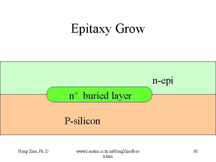
Epitaxy Grow n-epi n+ buried layer P-silicon Hong Xiao, Ph. D. www 2. austin. cc. tx. us/Hong. Xiao/Boo k. htm 60
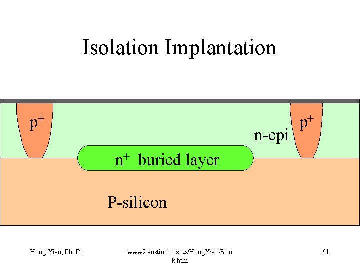
Isolation Implantation p+ n-epi p+ n+ buried layer P-silicon Hong Xiao, Ph. D. www 2. austin. cc. tx. us/Hong. Xiao/Boo k. htm 61
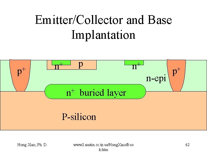
Emitter/Collector and Base Implantation p+ n+ p n+ n-epi p+ n+ buried layer P-silicon Hong Xiao, Ph. D. www 2. austin. cc. tx. us/Hong. Xiao/Boo k. htm 62
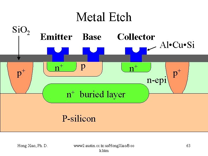
Metal Etch Si. O 2 Emitter p+ n+ Base Collector p Al • Cu • Si n+ n-epi p+ n+ buried layer P-silicon Hong Xiao, Ph. D. www 2. austin. cc. tx. us/Hong. Xiao/Boo k. htm 63
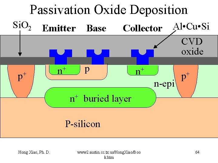
Passivation Oxide Deposition Si. O 2 Emitter Base Collector Al • Cu • Si CVD oxide p+ n+ p n+ n-epi p+ n+ buried layer P-silicon Hong Xiao, Ph. D. www 2. austin. cc. tx. us/Hong. Xiao/Boo k. htm 64
MOSFET • Good for digital electronics • Major driving forces: – Watches – Calculators – PC – Internet – Telecommunication Hong Xiao, Ph. D. www 2. austin. cc. tx. us/Hong. Xiao/Boo k. htm 65
1960 s: PMOS Process • • Bipolar dominated First MOSFET made in Bell Labs Silicon substrate Diffusion for doping – Boron diffuses faster in silicon – PMOS Hong Xiao, Ph. D. www 2. austin. cc. tx. us/Hong. Xiao/Boo k. htm 66
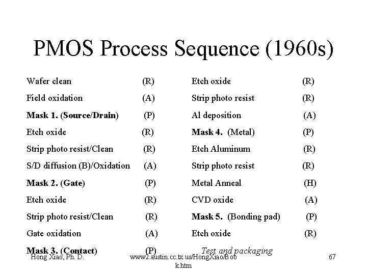
PMOS Process Sequence (1960 s) Wafer clean (R) Etch oxide (R) Field oxidation (A) Strip photo resist (R) Mask 1. (Source/Drain) (P) Al deposition (A) Etch oxide (R) Mask 4. (Metal) (P) Strip photo resist/Clean (R) Etch Aluminum (R) S/D diffusion (B)/Oxidation (A) Strip photo resist (R) Mask 2. (Gate) (P) Metal Anneal (H) Etch oxide (R) CVD oxide (A) Strip photo resist/Clean (R) Mask 5. (Bonding pad) (P) Gate oxidation (A) Etch oxide (R) Mask 3. (Contact) Hong Xiao, Ph. D. (P) Test and packaging www 2. austin. cc. tx. us/Hong. Xiao/Boo k. htm 67
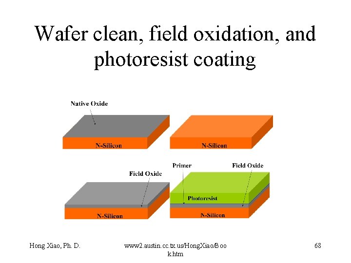
Wafer clean, field oxidation, and photoresist coating Hong Xiao, Ph. D. www 2. austin. cc. tx. us/Hong. Xiao/Boo k. htm 68
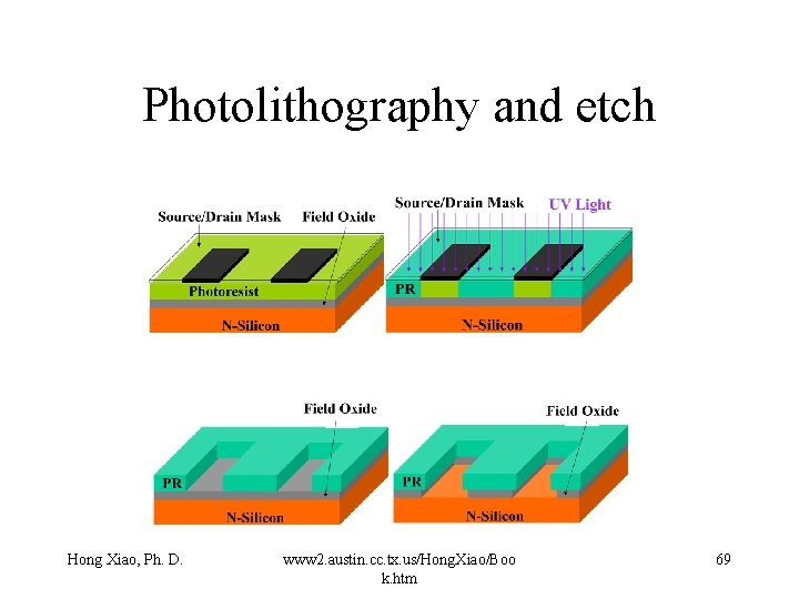
Photolithography and etch Hong Xiao, Ph. D. www 2. austin. cc. tx. us/Hong. Xiao/Boo k. htm 69
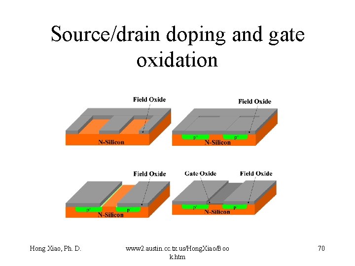
Source/drain doping and gate oxidation Hong Xiao, Ph. D. www 2. austin. cc. tx. us/Hong. Xiao/Boo k. htm 70
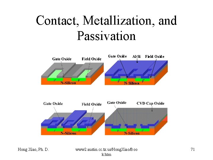
Contact, Metallization, and Passivation Gate Oxide p+ Hong Xiao, Ph. D. Al∙Si N-Silicon www 2. austin. cc. tx. us/Hong. Xiao/Boo k. htm Field Oxide p+ 71
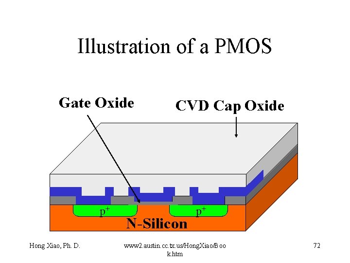
Illustration of a PMOS Gate Oxide p+ Hong Xiao, Ph. D. CVD Cap Oxide N-Silicon p+ www 2. austin. cc. tx. us/Hong. Xiao/Boo k. htm 72
NMOS Process after mid-1970 s • Doping: ion implantation replaced diffusion • NMOS replaced PMOS – NMOS is faster than PMOS • Self-aligned source/drain • Main driving force: watches and calculators Hong Xiao, Ph. D. www 2. austin. cc. tx. us/Hong. Xiao/Boo k. htm 73
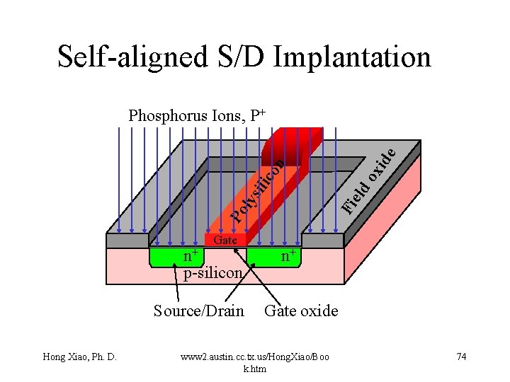
Self-aligned S/D Implantation Po Fi lys eld ili ox co n id e Phosphorus Ions, P+ Gate n+ p-silicon Source/Drain Hong Xiao, Ph. D. n+ Gate oxide www 2. austin. cc. tx. us/Hong. Xiao/Boo k. htm 74
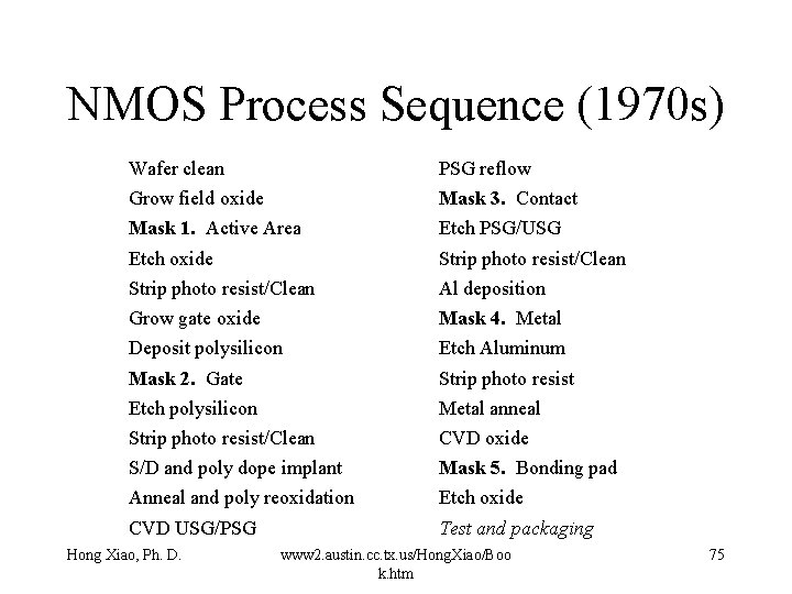
NMOS Process Sequence (1970 s) Wafer clean PSG reflow Grow field oxide Mask 3. Contact Mask 1. Active Area Etch PSG/USG Etch oxide Strip photo resist/Clean Al deposition Grow gate oxide Mask 4. Metal Deposit polysilicon Etch Aluminum Mask 2. Gate Strip photo resist Etch polysilicon Metal anneal Strip photo resist/Clean CVD oxide S/D and poly dope implant Mask 5. Bonding pad Anneal and poly reoxidation Etch oxide CVD USG/PSG Test and packaging Hong Xiao, Ph. D. www 2. austin. cc. tx. us/Hong. Xiao/Boo k. htm 75
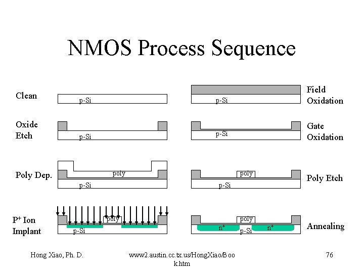
NMOS Process Sequence Clean Oxide Etch p-Si poly p-Si P+ Ion Implant poly Hong Xiao, Ph. D. Poly Etch p-Si poly p-Si Gate Oxidation p-Si Poly Dep. Field Oxidation poly n+ www 2. austin. cc. tx. us/Hong. Xiao/Boo k. htm p-Si n+ Annealing 76
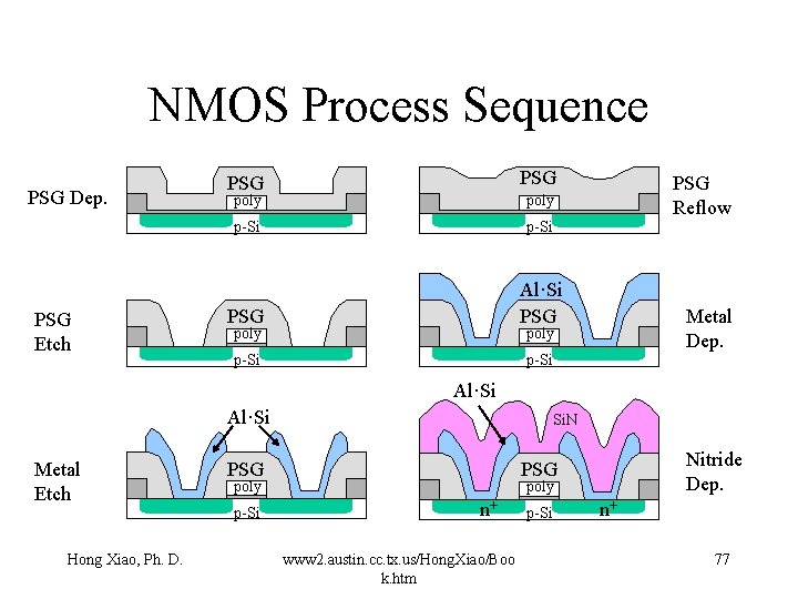
NMOS Process Sequence PSG Dep. PSG Etch PSG poly p-Si PSG Al·Si PSG p-Si poly PSG Reflow Metal Dep. poly Al·Si Metal Etch PSG Nitride Dep. PSG poly p-Si Hong Xiao, Ph. D. Si. N poly n+ www 2. austin. cc. tx. us/Hong. Xiao/Boo k. htm p-Si n+ 77
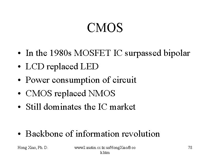
CMOS • • • In the 1980 s MOSFET IC surpassed bipolar LCD replaced LED Power consumption of circuit CMOS replaced NMOS Still dominates the IC market • Backbone of information revolution Hong Xiao, Ph. D. www 2. austin. cc. tx. us/Hong. Xiao/Boo k. htm 78
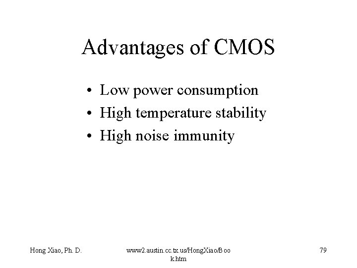
Advantages of CMOS • Low power consumption • High temperature stability • High noise immunity Hong Xiao, Ph. D. www 2. austin. cc. tx. us/Hong. Xiao/Boo k. htm 79
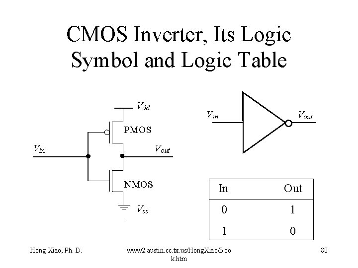
CMOS Inverter, Its Logic Symbol and Logic Table Vdd Vin Vout PMOS Vin Vout NMOS Vss Hong Xiao, Ph. D. In Out 0 1 1 0 www 2. austin. cc. tx. us/Hong. Xiao/Boo k. htm 80
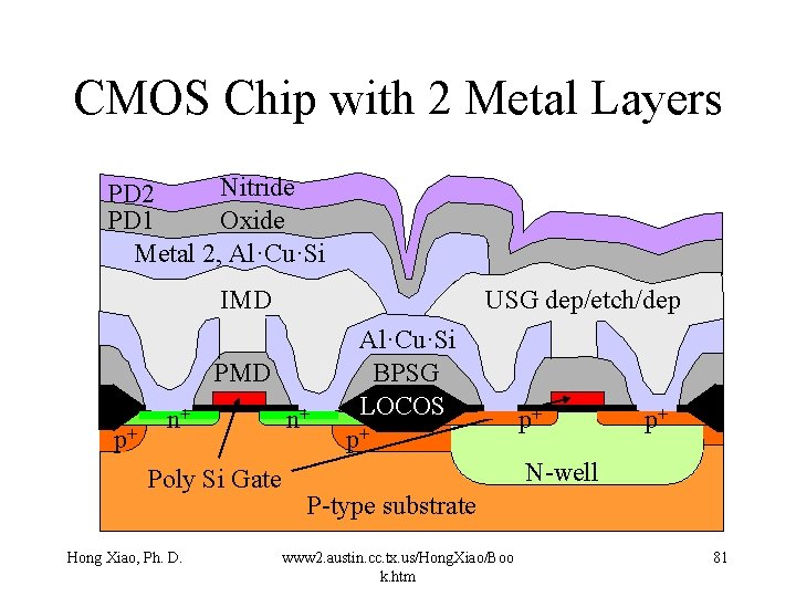
CMOS Chip with 2 Metal Layers Nitride PD 2 PD 1 Oxide Metal 2, Al·Cu·Si IMD USG dep/etch/dep PMD p+ n+ Poly Si Gate Hong Xiao, Ph. D. n+ Al·Cu·Si BPSG LOCOS Si. O 2 p+ p+ p+ N-well P-type substrate www 2. austin. cc. tx. us/Hong. Xiao/Boo k. htm 81
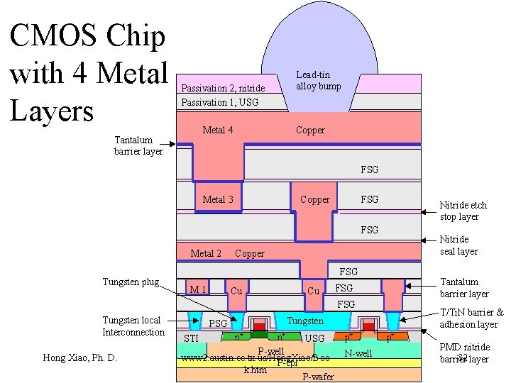
CMOS Chip with 4 Metal Layers Passivation 2, nitride Passivation 1, USG Metal 4 Tantalum barrier layer Lead-tin alloy bump Copper FSG Metal 3 Copper FSG Nitride etch stop layer FSG Metal 2 Tungsten plug Nitride seal layer Copper FSG M 1 Cu Cu Tantalum barrier layer FSG Tungsten local Interconnection Hong Xiao, Ph. D. PSG n+ USG P-well www 2. austin. cc. tx. us/Hong. Xiao/Boo P-epi k. htm P-wafer STI T/Ti. N barrier & adhesion layer Tungsten n+ p+ N-well p+ PMD nitride 82 layer barrier
Summary • Semiconductors are the materials with conductivity between conductor and insulator • Its conductivity can be controlled by dopant concentration and applied voltage • Silicon, germanium, and gallium arsenate • Silicon most popular: abundant and stable oxide Hong Xiao, Ph. D. www 2. austin. cc. tx. us/Hong. Xiao/Boo k. htm 83
Summary • Boron doped semiconductor is p-type, majority carriers are holes • P, As, or Sb doped semiconductor is p-type, the majority carriers are electrons • Higher dopant concentration, lower resistivity • At the same dopant concentration, n-type has lower resistivity than p-type Hong Xiao, Ph. D. www 2. austin. cc. tx. us/Hong. Xiao/Boo k. htm 84
Summary R=r l/A C=k A/d Capacitors are mainly used in DRAM Bipolar transistors can amplify electric signal, mainly used for analog systems • MOSFET electric controlled switch, mainly used for digital systems • • Hong Xiao, Ph. D. www 2. austin. cc. tx. us/Hong. Xiao/Boo k. htm 85
Summary • MOSFETs dominated IC industry since 1980 s • Three kinds IC chips microprocessor, memory, and ASIC • Advantages of CMOS: low power, high temperature stability, high noise immunity, and clocking simplicity Hong Xiao, Ph. D. www 2. austin. cc. tx. us/Hong. Xiao/Boo k. htm 86
Summary • The basic CMOS process steps are transistor making (front-end) and interconnection/passivation (back-end) • The most basic semiconductor processes are adding, removing, heating, and patterning processes. Hong Xiao, Ph. D. www 2. austin. cc. tx. us/Hong. Xiao/Boo k. htm 87
- Slides: 87