Chapter 3 A TopLevel View of Computer Function


- Slides: 35

Chapter 3 A Top-Level View of Computer Function and Interconnection +

+ Computer Components n Contemporary computer designs are based on concepts developed by John von Neumann at the Institute for Advanced Studies, Princeton n Referred to as the von Neumann architecture and is based on three key concepts: n n Data and instructions are stored in a single read-write memory n The contents of this memory are addressable by location, without regard to the type of data contained there n Execution occurs in a sequential fashion (unless explicitly modified) from one instruction to the next Hardwired program n The result of the process of connecting the various components in the desired configuration

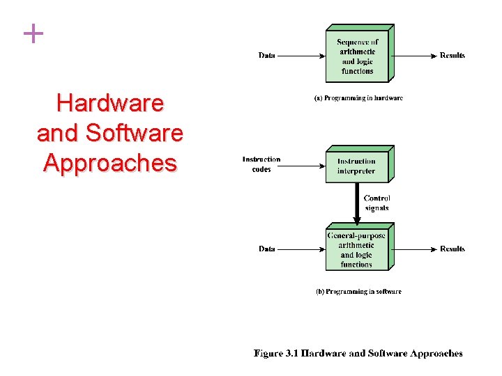
+ Hardware and Software Approaches

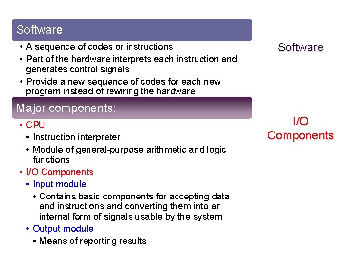
Software • A sequence of codes or instructions • Part of the hardware interprets each instruction and generates control signals • Provide a new sequence of codes for each new program instead of rewiring the hardware Software Major components: • CPU • Instruction interpreter • Module of general-purpose arithmetic and logic functions • I/O Components + • Input module • Contains basic components for accepting data and instructions and converting them into an internal form of signals usable by the system • Output module • Means of reporting results I/O Components

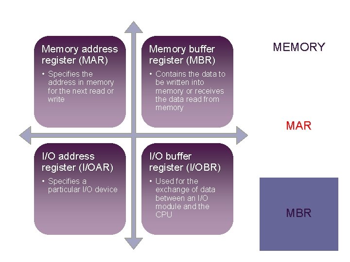
Memory address register (MAR) Memory buffer register (MBR) • Specifies the address in memory for the next read or write • Contains the data to be written into memory or receives the data read from memory MEMORY MAR + I/O address register (I/OAR) I/O buffer register (I/OBR) • Specifies a particular I/O device • Used for the exchange of data between an I/O module and the CPU MBR

Computer Components: Top Level View

+ Basic Instruction Cycle

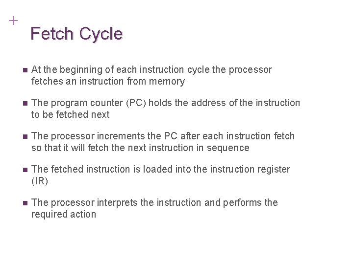
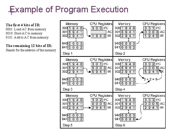
+ Fetch Cycle n At the beginning of each instruction cycle the processor fetches an instruction from memory n The program counter (PC) holds the address of the instruction to be fetched next n The processor increments the PC after each instruction fetch so that it will fetch the next instruction in sequence n The fetched instruction is loaded into the instruction register (IR) n The processor interprets the instruction and performs the required action

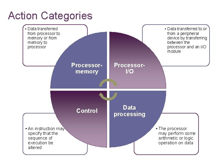
Action Categories • Data transferred from processor to memory or from memory to processor • An instruction may specify that the sequence of execution be altered • Data transferred to or from a peripheral device by transferring between the processor and an I/O module Processormemory Processor. I/O Control Data processing • The processor may perform some arithmetic or logic operation on data


Example of Program Execution + The first 4 bits of IR: 0001: Load AC from memory 0010: Store AC to memory 0101: Add to AC from memory The remaining 12 bits of IR: Stands for the address of the memory

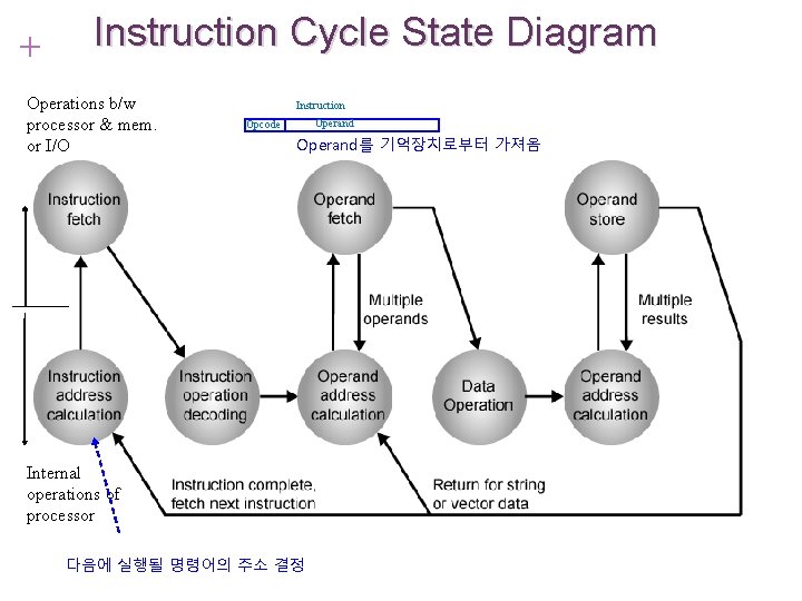
+ Instruction Cycle State Diagram Operations b/w processor & mem. or I/O Instruction Operand Opcode Operand를 기억장치로부터 가져옴 Internal operations of processor 다음에 실행될 명령어의 주소 결정

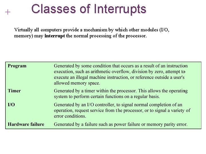
+ Classes of Interrupts Virtually all computers provide a mechanism by which other modules (I/O, memory) may interrupt the normal processing of the processor.

Program Flow Control

+ Transfer of Control via Interrupts When the interrupt processing is completed, execution resumes (Figure 3. 8). Thus, the user program does not have to contain any special code to accommodate interrupts; the processor and the operating system are responsible for suspending the user program and then resuming it at the same point.

+ Instruction Cycle With Interrupts

+ Program Timing: Short I/O Wait Figures 3. 7 b and 3. 10 b assume that the time required for the I/O operation is relatively short: less than the time to complete the execution of instructions between write operations in the user program. In this case, the segment of code labeled code segment 2 is interrupted. A portion of the code (2 a) executes (while the I/O operation is performed) and then the interrupt occurs (upon the completion of the I/O operation). After the interrupt is serviced, execution resumes with the remainder of code segment 2 (2 b).

+ Program Timing: Long I/O Wait The more typical case, especially for a slow device such as a printer, is that the I/O operation will take much more time than executing a sequence of user instructions. Figure 3. 7 c indicates this state of affairs. In this case, the user program reaches the second WRITE call before the I/O operation spawned by the first call is complete. The result is that the user program is hung up at that point.

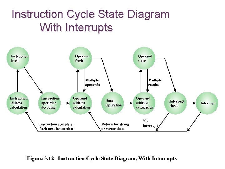
Instruction Cycle State Diagram With Interrupts

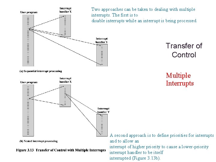
Two approaches can be taken to dealing with multiple interrupts. The first is to disable interrupts while an interrupt is being processed. Transfer of Control Multiple Interrupts + A second approach is to define priorities for interrupts and to allow an interrupt of higher priority to cause a lower-priority interrupt handler to be itself interrupted (Figure 3. 13 b).

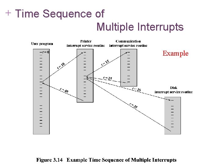
+ Time Sequence of Multiple Interrupts Example

+ I/O Function n I/O module can exchange data directly with the processor n Processor can read data from or write data to an I/O module n n Processor identifies a specific device that is controlled by a particular I/O module n I/O instructions rather than memory referencing instructions In some cases it is desirable to allow I/O exchanges to occur directly with memory n The processor grants to an I/O module the authority to read from or write to memory so that the I/O memory transfer can occur without tying up the processor n The I/O module issues read or write commands to memory relieving the processor of responsibility for the exchange n This operation is known as direct memory access (DMA)

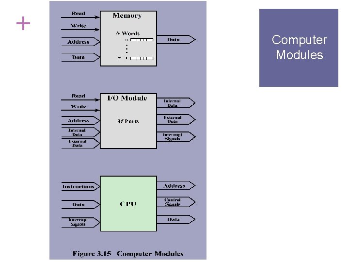
+ Computer Modules

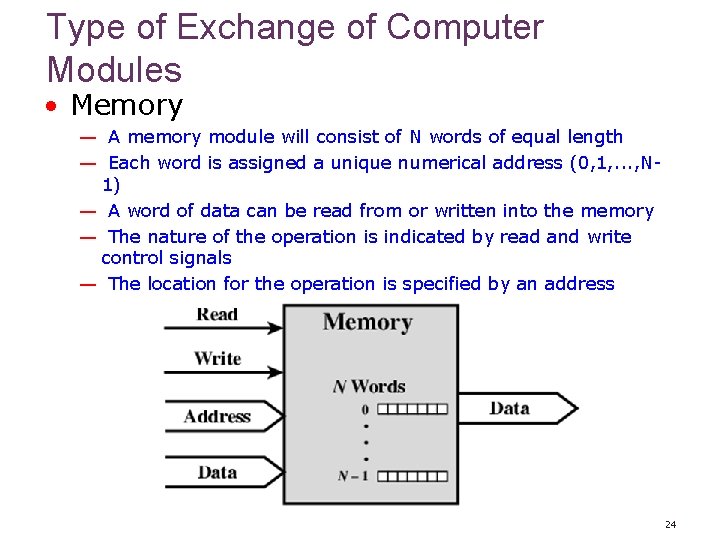
Type of Exchange of Computer Modules • Memory — A memory module will consist of N words of equal length — Each word is assigned a unique numerical address (0, 1, . . . , N 1) — A word of data can be read from or written into the memory — The nature of the operation is indicated by read and write control signals — The location for the operation is specified by an address 24

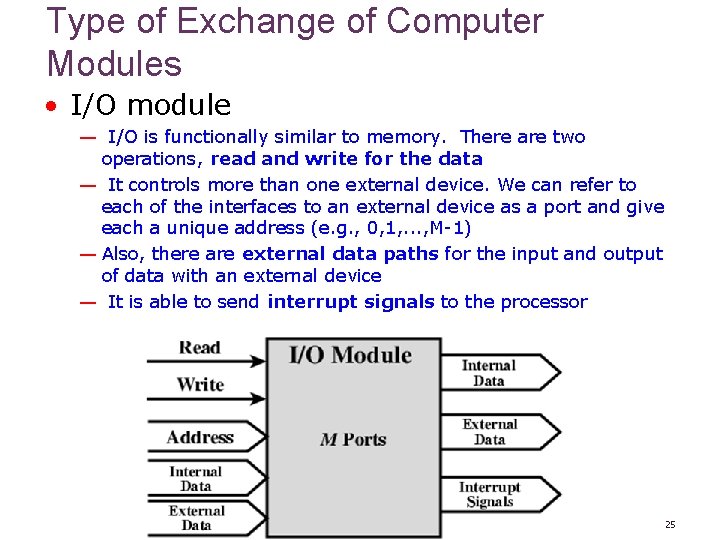
Type of Exchange of Computer Modules • I/O module — I/O is functionally similar to memory. There are two operations, read and write for the data — It controls more than one external device. We can refer to each of the interfaces to an external device as a port and give each a unique address (e. g. , 0, 1, . . . , M-1) — Also, there are external data paths for the input and output of data with an external device — It is able to send interrupt signals to the processor 25

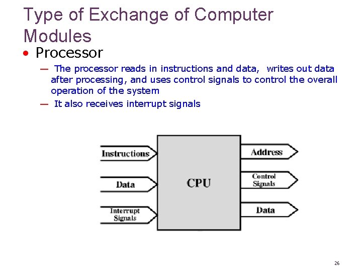
Type of Exchange of Computer Modules • Processor — The processor reads in instructions and data, writes out data after processing, and uses control signals to control the overall operation of the system — It also receives interrupt signals 26

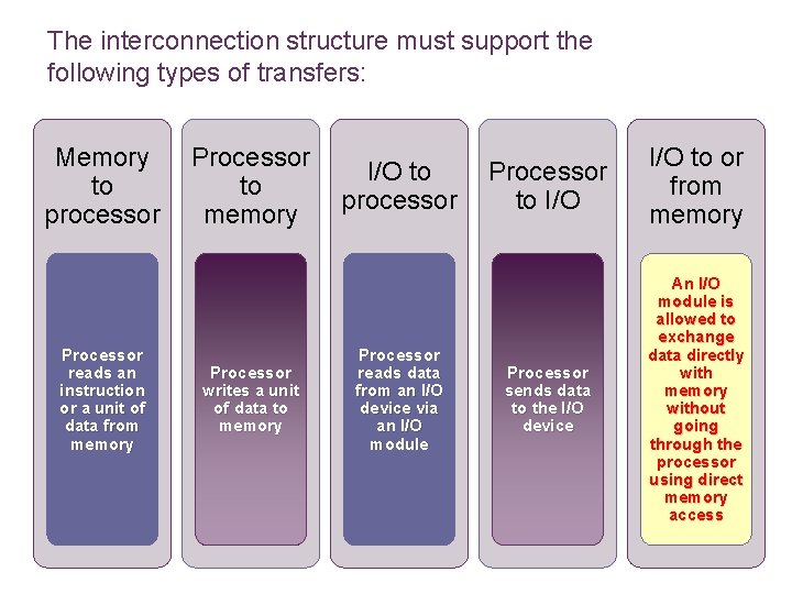
The interconnection structure must support the following types of transfers: Memory to processor Processor reads an instruction or a unit of data from memory Processor to memory Processor writes a unit of data to memory I/O to processor Processor reads data from an I/O device via an I/O module Processor to I/O to or from memory Processor sends data to the I/O device An I/O module is allowed to exchange data directly with memory without going through the processor using direct memory access

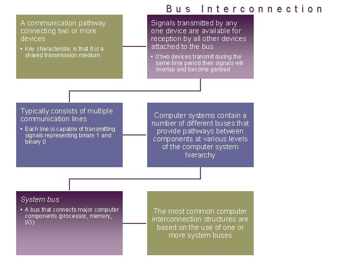
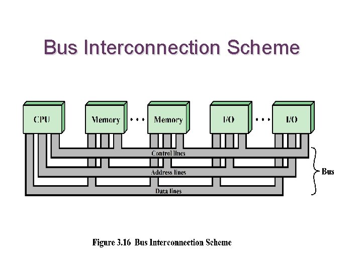
B u s A communication pathway connecting two or more devices • Key characteristic is that it is a shared transmission medium Typically consists of multiple communication lines • Each line is capable of transmitting signals representing binary 1 and binary 0 In te r c o n ne c t i on Signals transmitted by any one device are available for reception by all other devices attached to the bus • If two devices transmit during the same time period their signals will overlap and become garbled Computer systems contain a number of different buses that provide pathways between components at various levels of the computer system hierarchy System bus • A bus that connects major computer components (processor, memory, I/O) The most common computer interconnection structures are based on the use of one or more system buses

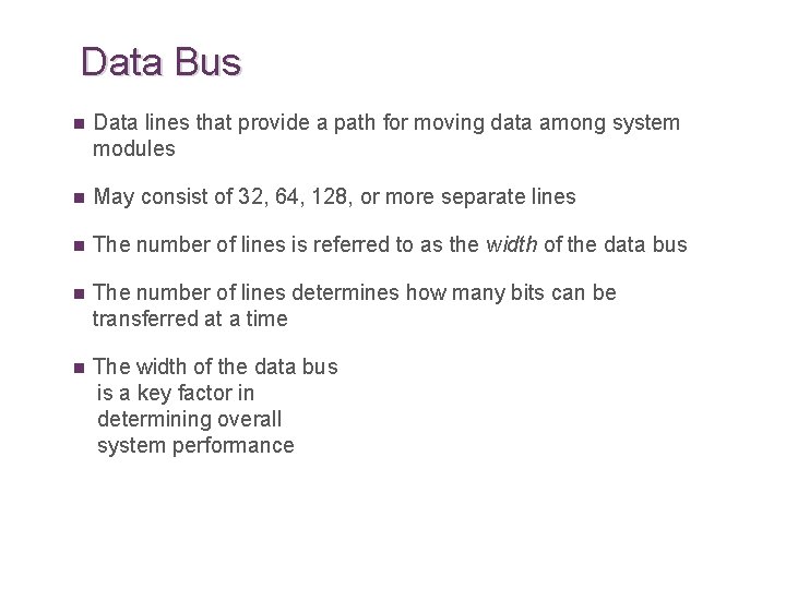
Data Bus n Data lines that provide a path for moving data among system modules n May consist of 32, 64, 128, or more separate lines n The number of lines is referred to as the width of the data bus n The number of lines determines how many bits can be transferred at a time n The width of the data bus is a key factor in determining overall system performance

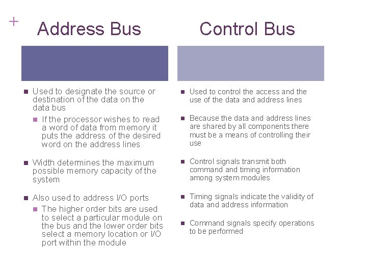
+ Address Bus Control Bus Used to designate the source or destination of the data on the data bus n If the processor wishes to read a word of data from memory it puts the address of the desired word on the address lines n Used to control the access and the use of the data and address lines n Because the data and address lines are shared by all components there must be a means of controlling their use n Width determines the maximum possible memory capacity of the system n Control signals transmit both command timing information among system modules n Also used to address I/O ports n The higher order bits are used to select a particular module on the bus and the lower order bits select a memory location or I/O port within the module n Timing signals indicate the validity of data and address information n Command signals specify operations to be performed n

Bus Interconnection Scheme

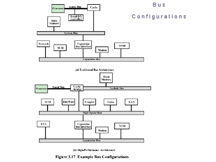
Bus Configurations

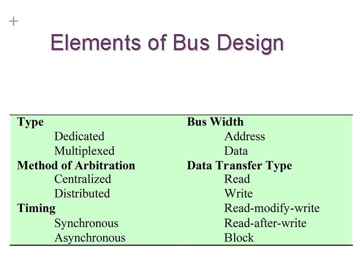
+ Elements of Bus Design

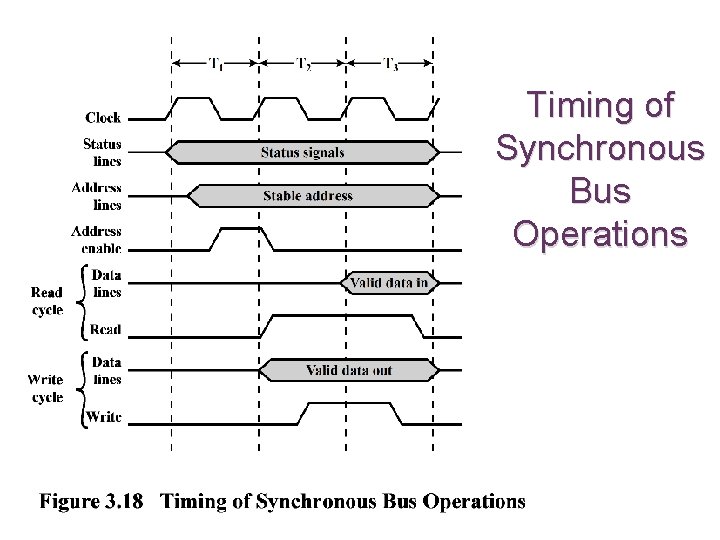
Timing of Synchronous Bus Operations

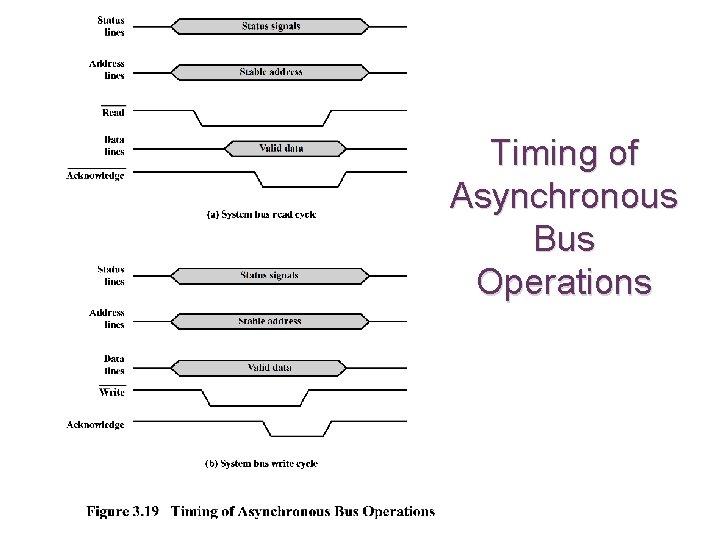
Timing of Asynchronous Bus Operations