Chapter 2 The Microprocessor and its Architecture The
![Defaults Convention Example: • • EA = CS: [IP] Default segment numbers in: – Defaults Convention Example: • • EA = CS: [IP] Default segment numbers in: –](https://slidetodoc.com/presentation_image_h2/3eb2dcbee844d5468120b5b848fb2965/image-17.jpg)



- Slides: 51

Chapter 2 The Microprocessor and its Architecture The Intel 8086, 80 X 86, and Pentium Family Brey: The Intel Microprocessors, 7 e © 2006 Pearson Education, Upper Saddle River, NJ 07458. All Rights Reserved.

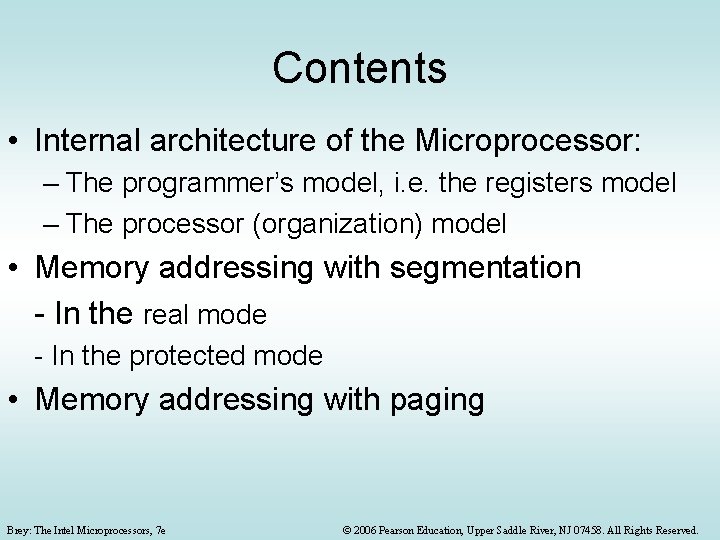
Contents • Internal architecture of the Microprocessor: – The programmer’s model, i. e. the registers model – The processor (organization) model • Memory addressing with segmentation - In the real mode - In the protected mode • Memory addressing with paging Brey: The Intel Microprocessors, 7 e © 2006 Pearson Education, Upper Saddle River, NJ 07458. All Rights Reserved.

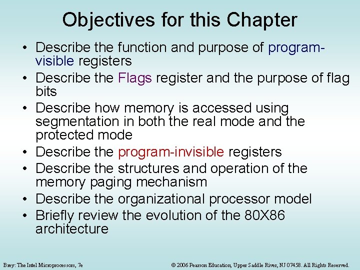
Objectives for this Chapter • Describe the function and purpose of programvisible registers • Describe the Flags register and the purpose of flag bits • Describe how memory is accessed using segmentation in both the real mode and the protected mode • Describe the program-invisible registers • Describe the structures and operation of the memory paging mechanism • Describe the organizational processor model • Briefly review the evolution of the 80 X 86 architecture Brey: The Intel Microprocessors, 7 e © 2006 Pearson Education, Upper Saddle River, NJ 07458. All Rights Reserved.

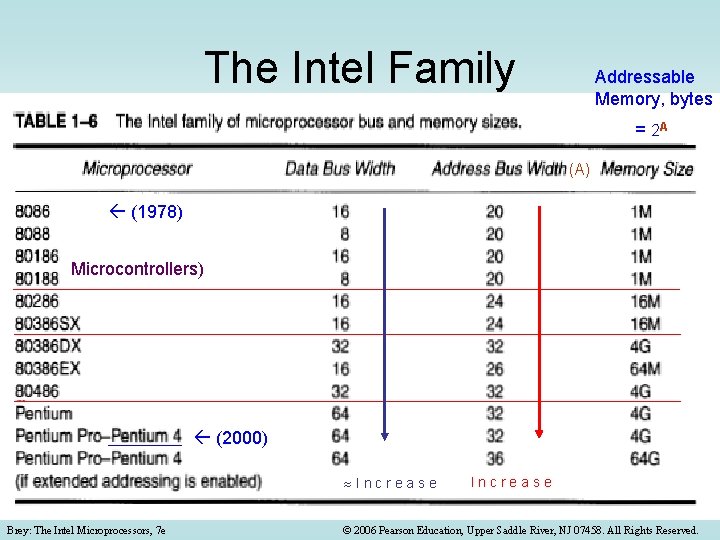
The Intel Family Addressable Memory, bytes = 2 A (A) (1978) Microcontrollers) (2000) Increase Brey: The Intel Microprocessors, 7 e Increase © 2006 Pearson Education, Upper Saddle River, NJ 07458. All Rights Reserved.

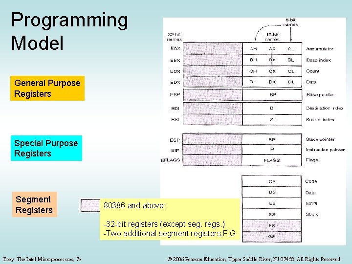
Programming Model General Purpose Registers Special Purpose Registers Segment Registers 80386 and above: -32 -bit registers (except seg. regs. ) -Two additional segment registers: F, G Brey: The Intel Microprocessors, 7 e © 2006 Pearson Education, Upper Saddle River, NJ 07458. All Rights Reserved.

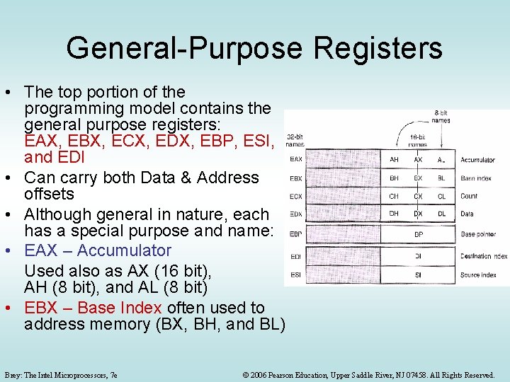
General-Purpose Registers • The top portion of the programming model contains the general purpose registers: EAX, EBX, ECX, EDX, EBP, ESI, and EDI • Can carry both Data & Address offsets • Although general in nature, each has a special purpose and name: • EAX – Accumulator Used also as AX (16 bit), AH (8 bit), and AL (8 bit) • EBX – Base Index often used to address memory (BX, BH, and BL) Brey: The Intel Microprocessors, 7 e © 2006 Pearson Education, Upper Saddle River, NJ 07458. All Rights Reserved.

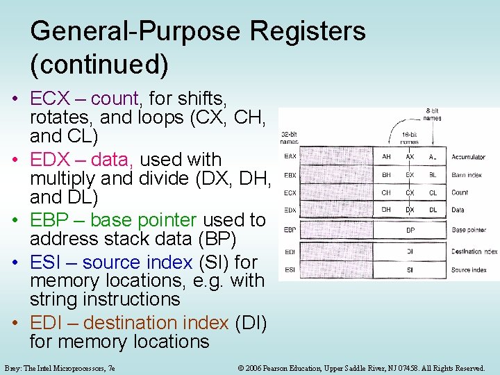
General-Purpose Registers (continued) • ECX – count, for shifts, rotates, and loops (CX, CH, and CL) • EDX – data, used with multiply and divide (DX, DH, and DL) • EBP – base pointer used to address stack data (BP) • ESI – source index (SI) for memory locations, e. g. with string instructions • EDI – destination index (DI) for memory locations Brey: The Intel Microprocessors, 7 e © 2006 Pearson Education, Upper Saddle River, NJ 07458. All Rights Reserved.

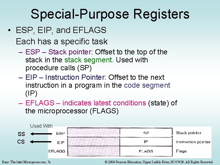
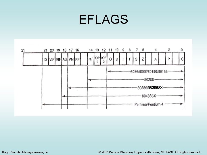
Special-Purpose Registers • ESP, EIP, and EFLAGS Each has a specific task – ESP – Stack pointer: Offset to the top of the stack in the stack segment. Used with procedure calls (SP) – EIP – Instruction Pointer: Offset to the next instruction in a program in the code segment (IP) – EFLAGS – indicates latest conditions (state) of the microprocessor (FLAGS) Used With SS CS Brey: The Intel Microprocessors, 7 e © 2006 Pearson Education, Upper Saddle River, NJ 07458. All Rights Reserved.

EFLAGS 80386 DX Brey: The Intel Microprocessors, 7 e © 2006 Pearson Education, Upper Saddle River, NJ 07458. All Rights Reserved.

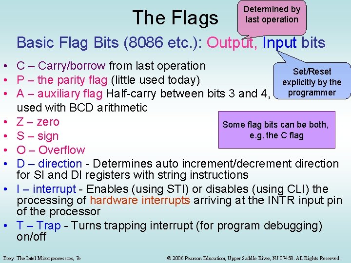
The Flags Determined by last operation Basic Flag Bits (8086 etc. ): Output, Input bits • C – Carry/borrow from last operation Set/Reset • P – the parity flag (little used today) explicitly by the • A – auxiliary flag Half-carry between bits 3 and 4, programmer used with BCD arithmetic • Z – zero Some flag bits can be both, e. g. the C flag • S – sign • O – Overflow • D – direction - Determines auto increment/decrement direction for SI and DI registers with string instructions • I – interrupt - Enables (using STI) or disables (using CLI) the processing of hardware interrupts arriving at the INTR input pin of the processor • T – Trap - Turns trapping interrupt (for program debugging) on/off Brey: The Intel Microprocessors, 7 e © 2006 Pearson Education, Upper Saddle River, NJ 07458. All Rights Reserved.

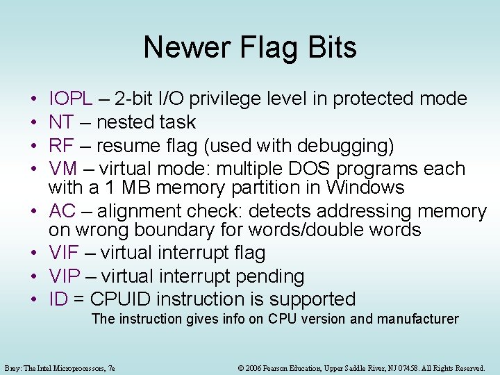
Newer Flag Bits • • IOPL – 2 -bit I/O privilege level in protected mode NT – nested task RF – resume flag (used with debugging) VM – virtual mode: multiple DOS programs each with a 1 MB memory partition in Windows AC – alignment check: detects addressing memory on wrong boundary for words/double words VIF – virtual interrupt flag VIP – virtual interrupt pending ID = CPUID instruction is supported The instruction gives info on CPU version and manufacturer Brey: The Intel Microprocessors, 7 e © 2006 Pearson Education, Upper Saddle River, NJ 07458. All Rights Reserved.

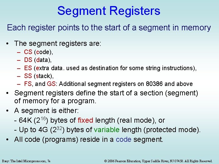
Segment Registers Each register points to the start of a segment in memory • The segment registers are: – – – CS (code), DS (data), ES (extra data. used as destination for some string instructions), SS (stack), FS, and GS: Additional segment registers on 80386 and above • Segment registers define the start of a section (segment) of memory for a program. • A segment is either: - 64 K (216) bytes of fixed length (real mode), or - Up to 4 G (232) bytes of variable length (protected mode). • All code (programs) reside in a code segment. Brey: The Intel Microprocessors, 7 e © 2006 Pearson Education, Upper Saddle River, NJ 07458. All Rights Reserved.

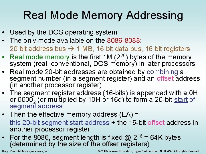
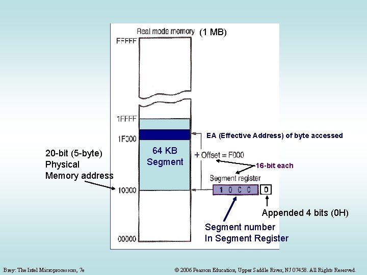
Real Mode Memory Addressing • Used by the DOS operating system • The only mode available on the 8086 -8088: 20 bit address bus 1 MB, 16 bit data bus, 16 bit registers • Real mode memory is the first 1 M (220) bytes of the memory system (real, conventional, DOS memory) in later processors • Real mode 20 -bit addresses are obtained by combining a segment number (in a segment register) and an offset address (in another processor register) • The segment register address (16 -bits) is appended with a 0 H or 00002 (or multiplied by 10 H or 16 d) to form a 20 -bit start of segment address • Then the effective memory address (EA) = this 20 -bit segment start address + the 16 -bit offset address in another processor register • For the 8086, segment length is fixed @ 216 = 64 K bytes (determined by the size of the offset registers) Brey: The Intel Microprocessors, 7 e © 2006 Pearson Education, Upper Saddle River, NJ 07458. All Rights Reserved.

MB (11 MB) EA (Effective Address) of byte accessed 20 -bit (5 -byte) Physical Memory address 64 KB Segment + 16 -bit each Appended 4 bits (0 H) Segment number In Segment Register Brey: The Intel Microprocessors, 7 e © 2006 Pearson Education, Upper Saddle River, NJ 07458. All Rights Reserved.

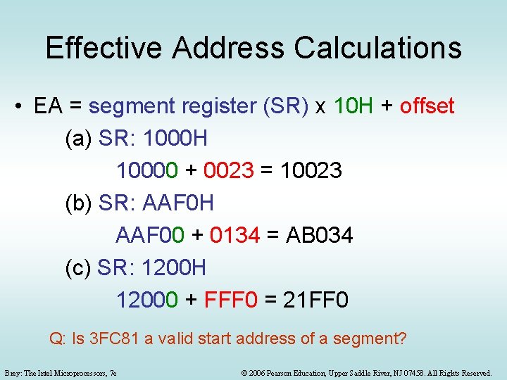
Effective Address Calculations • EA = segment register (SR) x 10 H + offset (a) SR: 1000 H 10000 + 0023 = 10023 (b) SR: AAF 0 H AAF 00 + 0134 = AB 034 (c) SR: 1200 H 12000 + FFF 0 = 21 FF 0 Q: Is 3 FC 81 a valid start address of a segment? Brey: The Intel Microprocessors, 7 e © 2006 Pearson Education, Upper Saddle River, NJ 07458. All Rights Reserved.

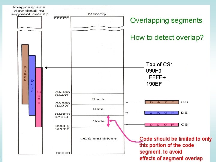
Overlapping segments How to detect overlap? Top of CS: 090 F 0 FFFF+ 190 EF Brey: The Intel Microprocessors, 7 e Code should be limited to only this portion of the code segment, to avoid segment © 2006 Pearson Education, effects Upper Saddleof River, NJ 07458. Alloverlap Rights Reserved.
![Defaults Convention Example EA CS IP Default segment numbers in Defaults Convention Example: • • EA = CS: [IP] Default segment numbers in: –](https://slidetodoc.com/presentation_image_h2/3eb2dcbee844d5468120b5b848fb2965/image-17.jpg)
Defaults Convention Example: • • EA = CS: [IP] Default segment numbers in: – CS for program (code) Segment number in Segment register – SS for stack – DS for data – ES for string (destination) data Default offset addresses that go with them: Segment Offset (16 -bit) 8080, 8086, 80286 Offset: Literal or in a CPU register Offset (32 -bit) 80386 and above Purpose CS SS DS IP EIP Program SP, BP ESP, EBP Stack BX, DI, SI, 8 -bit or 16 -bit # EBX, EDI, ESI, EAX ECX, EDX, 8 -bit or 32 -bit # Data ES DI, with string instructions EDI, with string instructions String destination Brey: The Intel Microprocessors, 7 e © 2006 Pearson Education, Upper Saddle River, NJ 07458. All Rights Reserved.

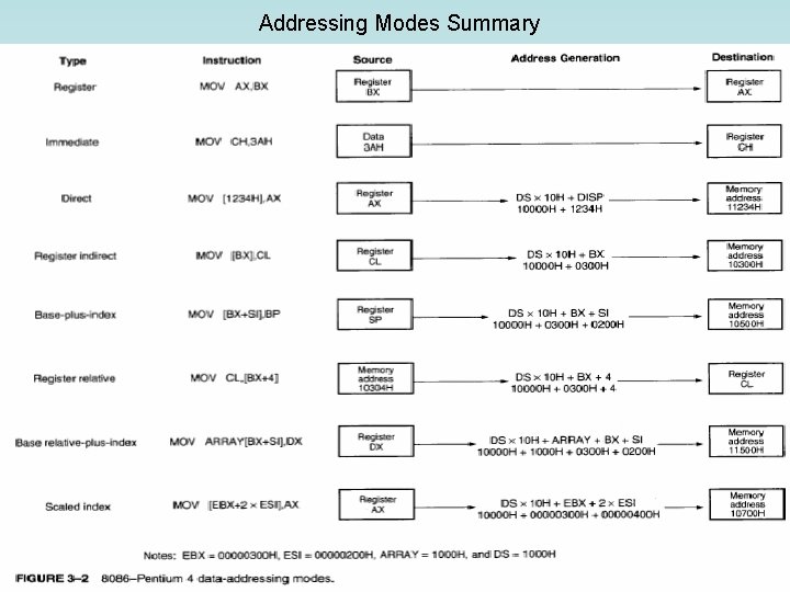
Addressing Modes Summary Brey: The Intel Microprocessors, 7 e © 2006 Pearson Education, Upper Saddle River, NJ 07458. All Rights Reserved.

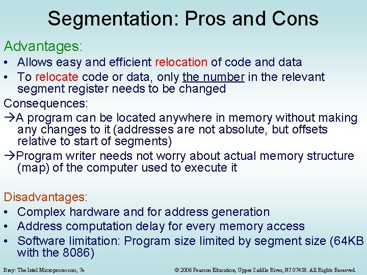
Segmentation: Pros and Cons Advantages: • Allows easy and efficient relocation of code and data • To relocate code or data, only the number in the relevant segment register needs to be changed Consequences: A program can be located anywhere in memory without making any changes to it (addresses are not absolute, but offsets relative to start of segments) Program writer needs not worry about actual memory structure (map) of the computer used to execute it Disadvantages: • Complex hardware and for address generation • Address computation delay for every memory access • Software limitation: Program size limited by segment size (64 KB with the 8086) Brey: The Intel Microprocessors, 7 e © 2006 Pearson Education, Upper Saddle River, NJ 07458. All Rights Reserved.

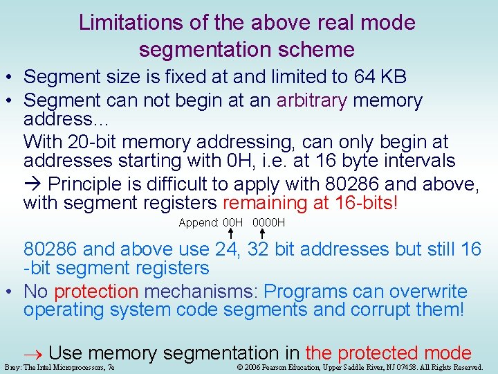
Limitations of the above real mode segmentation scheme • Segment size is fixed at and limited to 64 KB • Segment can not begin at an arbitrary memory address… With 20 -bit memory addressing, can only begin at addresses starting with 0 H, i. e. at 16 byte intervals Principle is difficult to apply with 80286 and above, with segment registers remaining at 16 -bits! Append: 00 H 0000 H 80286 and above use 24, 32 bit addresses but still 16 -bit segment registers • No protection mechanisms: Programs can overwrite operating system code segments and corrupt them! Use memory segmentation in the protected mode Brey: The Intel Microprocessors, 7 e © 2006 Pearson Education, Upper Saddle River, NJ 07458. All Rights Reserved.

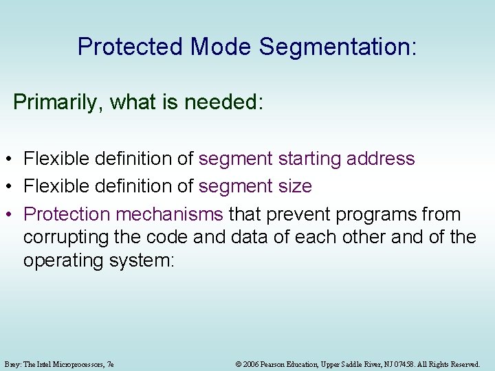
Protected Mode Segmentation: Primarily, what is needed: • Flexible definition of segment starting address • Flexible definition of segment size • Protection mechanisms that prevent programs from corrupting the code and data of each other and of the operating system: Brey: The Intel Microprocessors, 7 e © 2006 Pearson Education, Upper Saddle River, NJ 07458. All Rights Reserved.

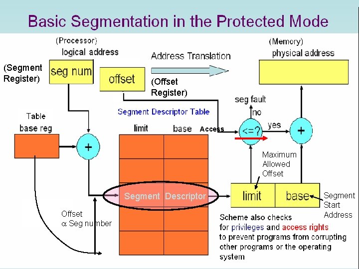
Basic Segmentation in the Protected Mode (Processor) (Memory) Address Translation (Segment Register) (Offset Register) Segment Descriptor Table Access Maximum Allowed Offset Segment Descriptor Offset Seg number Brey: The Intel Microprocessors, 7 e Segment Start Scheme also checks Address for privileges and access rights to prevent programs from corrupting other programs or the operating system © 2006 Pearson Education, Upper Saddle River, NJ 07458. All Rights Reserved.

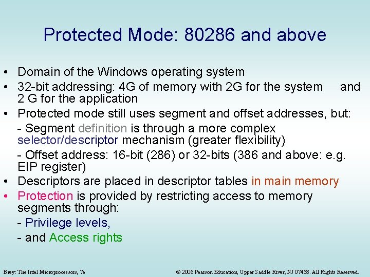
Protected Mode: 80286 and above • Domain of the Windows operating system • 32 -bit addressing: 4 G of memory with 2 G for the system and 2 G for the application • Protected mode still uses segment and offset addresses, but: - Segment definition is through a more complex selector/descriptor mechanism (greater flexibility) - Offset address: 16 -bit (286) or 32 -bits (386 and above: e. g. EIP register) • Descriptors are placed in descriptor tables in main memory • Protection is provided by restricting access to memory segments through: - Privilege levels, - and Access rights Brey: The Intel Microprocessors, 7 e © 2006 Pearson Education, Upper Saddle River, NJ 07458. All Rights Reserved.

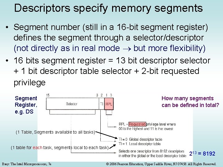
Descriptors specify memory segments • Segment number (still in a 16 -bit segment register) defines the segment through a selector/descriptor (not directly as in real mode but more flexibility) • 16 bits segment register = 13 bit descriptor selector + 1 bit descriptor table selector + 2 -bit requested privilege Segment Register, e. g. DS How many segments can be defined in total? (1 Table, Segments available to all tasks) (1 table for each task, segments local to each task) 213 = 8192 Brey: The Intel Microprocessors, 7 e © 2006 Pearson Education, Upper Saddle River, NJ 07458. All Rights Reserved.

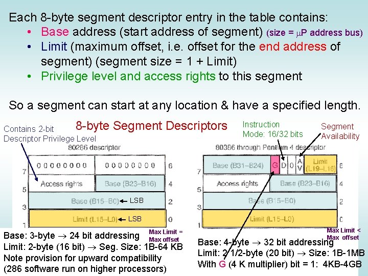
Each 8 -byte segment descriptor entry in the table contains: • Base address (start address of segment) (size = m. P address bus) • Limit (maximum offset, i. e. offset for the end address of segment) (segment size = 1 + Limit) • Privilege level and access rights to this segment So a segment can start at any location & have a specified length. 8 -byte Contains 2 -bit Descriptor Privilege Level Segment Descriptors Instruction Mode: 16/32 bits Segment Availability LSB Max Limit < Limit = Base: 3 -byte 24 bit addressing Max offset Base: 4 -byte 32 bit addressing Limit: 2 -byte (16 bit) Seg. Size: 1 B-64 KB Limit: 2 1/2 -byte (20 bit) Size: 1 B-1 MB Note provision for upward compatibility With G (4 K multiplier) bit = 1: 4 KB-4 GB (286 Thesoftware run on Brey: Intel Microprocessors, 7 e higher processors) © 2006 Pearson Education, Upper Saddle River, NJ 07458. All Rights Reserved.

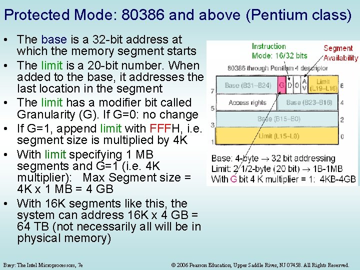
Protected Mode: 80386 and above (Pentium class) • The base is a 32 -bit address at which the memory segment starts • The limit is a 20 -bit number. When added to the base, it addresses the last location in the segment • The limit has a modifier bit called Granularity (G). If G=0: no change • If G=1, append limit with FFFH, i. e. segment size is multiplied by 4 K • With limit specifying 1 MB segments and G=1 (i. e. 4 K multiplier): Max Segment size = 4 K x 1 MB = 4 GB • With 16 K segments like this, the system can address 16 K x 4 GB = 64 TB (not necessarily all will be in physical memory) Brey: The Intel Microprocessors, 7 e © 2006 Pearson Education, Upper Saddle River, NJ 07458. All Rights Reserved.

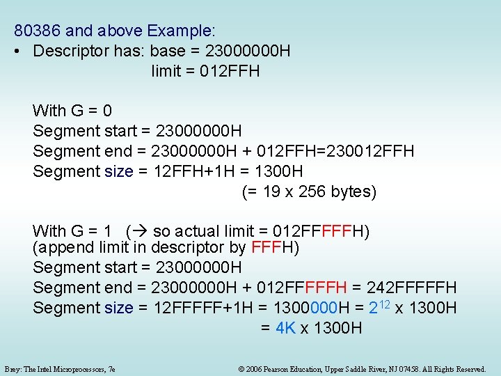
80386 and above Example: • Descriptor has: base = 23000000 H limit = 012 FFH With G = 0 Segment start = 23000000 H Segment end = 23000000 H + 012 FFH=230012 FFH Segment size = 12 FFH+1 H = 1300 H (= 19 x 256 bytes) With G = 1 ( so actual limit = 012 FFFFFH) (append limit in descriptor by FFFH) Segment start = 23000000 H Segment end = 23000000 H + 012 FFFFFH = 242 FFFFFH Segment size = 12 FFFFF+1 H = 1300000 H = 212 x 1300 H = 4 K x 1300 H Brey: The Intel Microprocessors, 7 e © 2006 Pearson Education, Upper Saddle River, NJ 07458. All Rights Reserved.

Protected Mode Segmentation Example Because each descriptor in the table is 8 bytes wide, Selector: 000 b is used as an offset from GDT (or LDT) base address to point to the start of the required segment descriptor Processor: 80286 (in main memory) Always 0’s for Descriptor # 2 upward compatibility 8 -byte Segment Descriptor # 1 Access Rights byte MSB 16 -bit Segment Register H 24 -bit Address 000 b Base Limit Offset Segment size = Limit+1 = FF+1 = 100 H bytes Descriptor # 0 What is the RPL value? GDT Base Address What is the selector value? Are we using the global or the local descriptor? table? (= segment #) Brey: The Intel Microprocessors, 7 e © 2006 Pearson Education, Upper Saddle River, NJ 07458. All Rights Reserved.

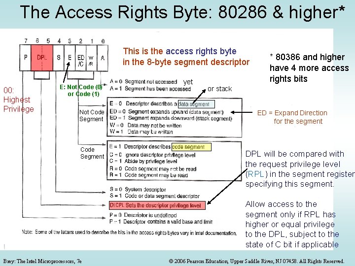
The Access Rights Byte: 80286 & higher* W /R 00: Highest Privilege E: Not Code (0) or Code (1) Not Code Segment This is the access rights byte in the 8 -byte segment descriptor yet * 80386 and higher have 4 more access rights bits or stack ED = Expand Direction for the segment DPL will be compared with the request privilege level (RPL) in the segment register specifying this segment. Allow access to the segment only if RPL has higher or equal privilege to the DPL, subject to the state of C bit if applicable Brey: The Intel Microprocessors, 7 e © 2006 Pearson Education, Upper Saddle River, NJ 07458. All Rights Reserved.

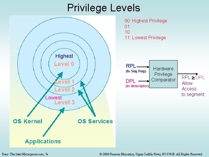
Privilege Levels 00: Highest Privilege 01 10 11: Lowest Privilege Highest RPL (In Seg Reg) DPL (in descriptor) Lowest Brey: The Intel Microprocessors, 7 e Hardware Privilege Comparator RPL DPL Allow Access to segment © 2006 Pearson Education, Upper Saddle River, NJ 07458. All Rights Reserved.

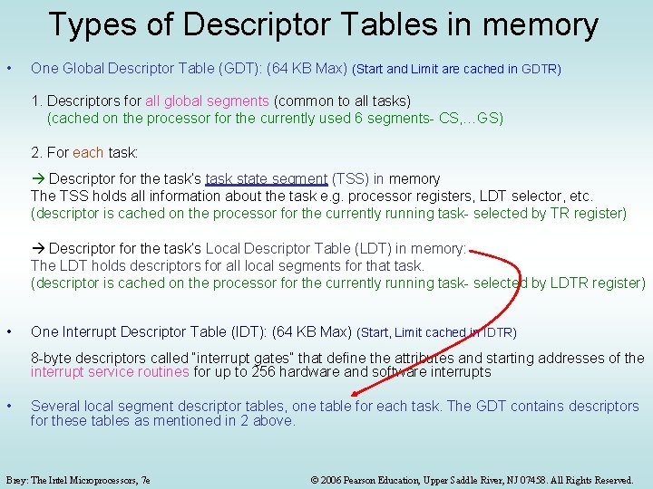
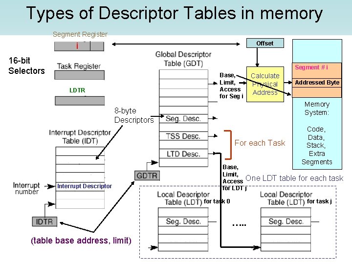
Types of Descriptor Tables in memory • One Global Descriptor Table (GDT): (64 KB Max) (Start and Limit are cached in GDTR) 1. Descriptors for all global segments (common to all tasks) (cached on the processor for the currently used 6 segments- CS, …GS) 2. For each task: Descriptor for the task’s task state segment (TSS) in memory The TSS holds all information about the task e. g. processor registers, LDT selector, etc. (descriptor is cached on the processor for the currently running task- selected by TR register) Descriptor for the task’s Local Descriptor Table (LDT) in memory: The LDT holds descriptors for all local segments for that task. (descriptor is cached on the processor for the currently running task- selected by LDTR register) • One Interrupt Descriptor Table (IDT): (64 KB Max) (Start, Limit cached in IDTR) 8 -byte descriptors called “interrupt gates” that define the attributes and starting addresses of the interrupt service routines for up to 256 hardware and software interrupts • Several local segment descriptor tables, one table for each task. The GDT contains descriptors for these tables as mentioned in 2 above. Brey: The Intel Microprocessors, 7 e © 2006 Pearson Education, Upper Saddle River, NJ 07458. All Rights Reserved.

Types of Descriptor Tables in memory Segment Register Offset i 16 -bit Selectors Segment # i Base, Limit, Access for Seg i LDTR Calculate Physical Address Memory System: 8 -byte Descriptors For each Task number Interrupt Descriptor Addressed Byte Base, Limit, Access One for LDT j Code, Data, Stack, Extra Segments LDT table for each task for task j for task 0 …. . (table base address, limit) Brey: The Intel Microprocessors, 7 e © 2006 Pearson Education, Upper Saddle River, NJ 07458. All Rights Reserved.

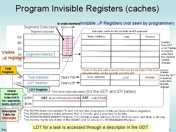
Program Invisible Registers (caches) In main memory. Invisible Segment Descriptor m. P Registers (not seen by programmer) Descriptor cache for the currently used 6 segments Loaded from GDT or LDT tables In memory every time the segment number changes Visible Segment Selector mp registers Task Register Global Descriptor Table (GDT) for: segments, tasks, and LDT Task Selector Task’s TSS LDT Selector Task’s LDT Register GDT Cache for the task state segment (TSS) and the descriptor of the local segment Loaded descriptor table - for the currently executing task from the GDT In memory every time the task changes (for the GDT and IDT tables) (24 or 32 bits) GDT (16 -bit) Descriptor Table for interrupts LDT for a task is accessed© through a descriptor in the GDT 2006 Pearson Education, Upper Saddle River, NJ 07458. All Rights Reserved. Brey: The Intel Microprocessors, 7 e

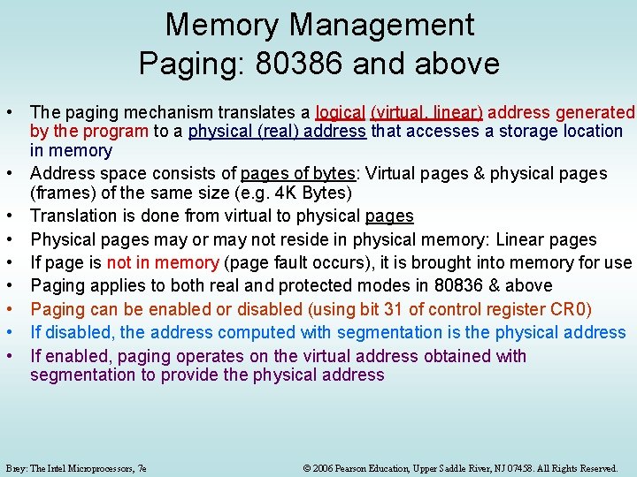
Memory Management Paging: 80386 and above • The paging mechanism translates a logical (virtual, linear) address generated by the program to a physical (real) address that accesses a storage location in memory • Address space consists of pages of bytes: Virtual pages & physical pages (frames) of the same size (e. g. 4 K Bytes) • Translation is done from virtual to physical pages • Physical pages may or may not reside in physical memory: Linear pages • If page is not in memory (page fault occurs), it is brought into memory for use • Paging applies to both real and protected modes in 80836 & above • Paging can be enabled or disabled (using bit 31 of control register CR 0) • If disabled, the address computed with segmentation is the physical address • If enabled, paging operates on the virtual address obtained with segmentation to provide the physical address Brey: The Intel Microprocessors, 7 e © 2006 Pearson Education, Upper Saddle River, NJ 07458. All Rights Reserved.

Example of 1 -level Paging: Address Translation (in the Memory Management Unit- MMU) Logical Pages, Each = 4 KB Logical, Linear, Virtual, Programmer Address (Memory) (From Processor) 32 bit byte address Physical frames (pages), Each = 4 KB Same offset 1 -Level Paging “Frames” are physical pages Physical Byte Address # Logical Page # Brey: The Intel Microprocessors, 7 e (To Memory)/ or Get from HD - Page table maps logical page #s to corresponding physical frame #’s - Offset part is the same for 07458. both © 2006 Pearson Education, Upper Saddle River, NJ All Rights Reserved.

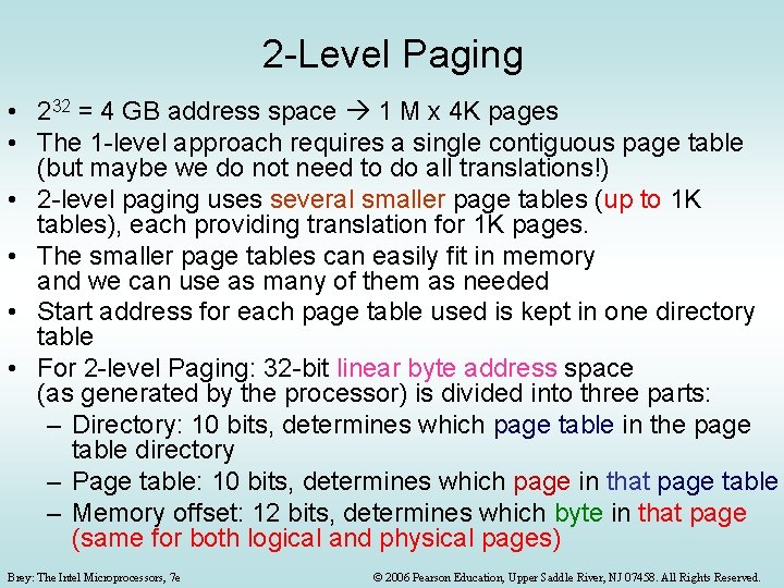
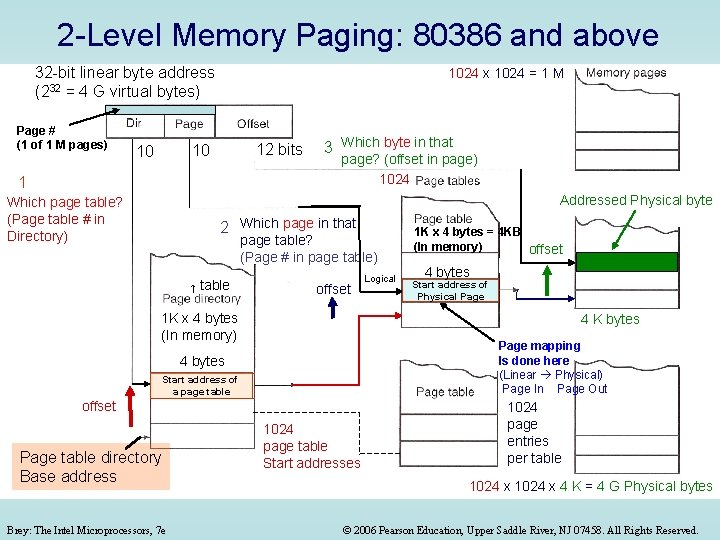
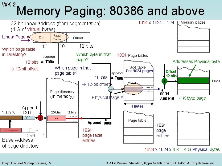
2 -Level Paging • 232 = 4 GB address space 1 M x 4 K pages • The 1 -level approach requires a single contiguous page table (but maybe we do not need to do all translations!) • 2 -level paging uses several smaller page tables (up to 1 K tables), each providing translation for 1 K pages. • The smaller page tables can easily fit in memory and we can use as many of them as needed • Start address for each page table used is kept in one directory table • For 2 -level Paging: 32 -bit linear byte address space (as generated by the processor) is divided into three parts: – Directory: 10 bits, determines which page table in the page table directory – Page table: 10 bits, determines which page in that page table – Memory offset: 12 bits, determines which byte in that page (same for both logical and physical pages) Brey: The Intel Microprocessors, 7 e © 2006 Pearson Education, Upper Saddle River, NJ 07458. All Rights Reserved.

2 -Level Memory Paging: 80386 and above 32 -bit linear byte address (232 = 4 G virtual bytes) Page # (1 of 1 M pages) 1024 x 1024 = 1 M 12 bits 10 10 1 3 Which byte in that page? (offset in page) 1024 Addressed Physical byte Which page table? (Page table # in Directory) 2 Which page in that page table? (Page # in page table) table offset 1 K x 4 bytes (In memory) Page mapping Is done here (Linear Physical) Page In Page Out Start address of a page table offset Brey: The Intel Microprocessors, 7 e 4 bytes Start address of Physical Page 4 K bytes 4 bytes Page table directory Base address Logical 1 K x 4 bytes = 4 KB (In memory) offset 1024 page table Start addresses 1024 page entries per table 1024 x 4 K = 4 G Physical bytes © 2006 Pearson Education, Upper Saddle River, NJ 07458. All Rights Reserved.

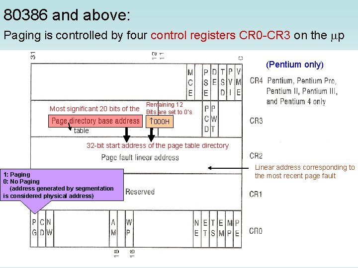
80386 and above: Paging is controlled by four control registers CR 0 -CR 3 on the mp (Pentium only) Remaining 12 Most significant 20 bits of the Bits are set to 0’s 000 H table 32 -bit start address of the page table directory 1: Paging 0: No Paging (address generated by segmentation is considered physical address) Brey: The Intel Microprocessors, 7 e Linear address corresponding to the most recent page fault © 2006 Pearson Education, Upper Saddle River, NJ 07458. All Rights Reserved.

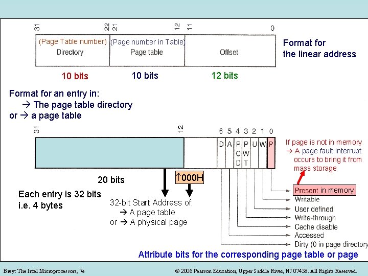
(Page Table number) (Page number in Table) 10 bits Format for the linear address 12 bits Format for an entry in: The page table directory or a page table 20 bits 000 H Each entry is 32 bits 32 -bit Start Address of: i. e. 4 bytes If page is not in memory A page fault interrupt occurs to bring it from mass storage in memory A page table or A physical page Attribute bits for the corresponding page table or page Brey: The Intel Microprocessors, 7 e © 2006 Pearson Education, Upper Saddle River, NJ 07458. All Rights Reserved.

WK 2 Memory Paging: 80386 and above 1024 x 1024 = 1 M 32 bit linear address (from segmentation) (4 G of virtual bytes) Page Table Linear Page # 12 bits 10 10 Which page table in Directory? Which byte in that page? Append 00 b 10 bits Which page in that page table? 12 -bit offset 1024 Addressed Physical byte Append 10 bits For 1024 pages 00 b 12 -bit offset 20 bits + (In memory) 20 bits Append 12 bits 000 H Offset 12 bits + 000 H Append Physical Page # 1 byte 4 K byte page 4 bytes 20 bits + CR 3 Base Address 000 H of page directory Brey: The Intel Microprocessors, 7 e 12 bits Append 000 H 1024 page table entries 1024 page entries 1024 x 4 K = 4 G Physical bytes © 2006 Pearson Education, Upper Saddle River, NJ 07458. All Rights Reserved.

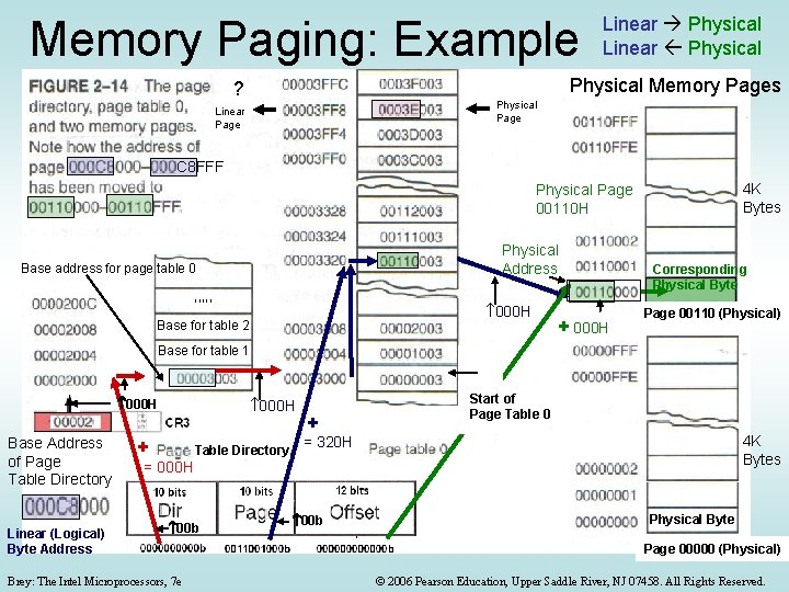
Memory Paging: Example Linear Physical Memory Pages ? Physical Page Linear Page C 8 FFF 4 K Bytes Physical Page 00110 H Physical Address Base address for page table 0 , , , 000 H Base for table 2 + 000 H Corresponding Physical Byte Page 00110 (Physical) Base for table 1 12 bits 000 H Base Address of Page Table Directory Linear (Logical) Byte Address 20 bits + + = 000 H Table Directory 00 b Brey: The Intel Microprocessors, 7 e 000 H + Start of Page Table 0 4 K Bytes = 320 H 00 b Physical Byte Page 00000 (Physical) © 2006 Pearson Education, Upper Saddle River, NJ 07458. All Rights Reserved.

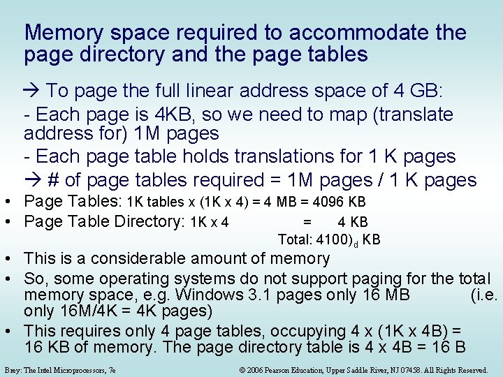
Memory space required to accommodate the page directory and the page tables To page the full linear address space of 4 GB: - Each page is 4 KB, so we need to map (translate address for) 1 M pages - Each page table holds translations for 1 K pages # of page tables required = 1 M pages / 1 K pages • Page Tables: 1 K tables x (1 K x 4) = 4 MB = 4096 KB • Page Table Directory: 1 K x 4 = 4 KB Total: 4100) d KB • This is a considerable amount of memory • So, some operating systems do not support paging for the total memory space, e. g. Windows 3. 1 pages only 16 MB (i. e. only 16 M/4 K = 4 K pages) • This requires only 4 page tables, occupying 4 x (1 K x 4 B) = 16 KB of memory. The page directory table is 4 x 4 B = 16 B Brey: The Intel Microprocessors, 7 e © 2006 Pearson Education, Upper Saddle River, NJ 07458. All Rights Reserved.

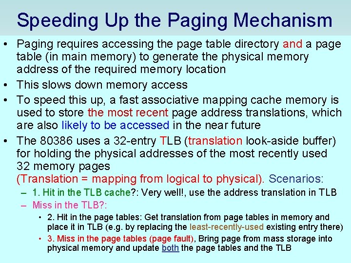
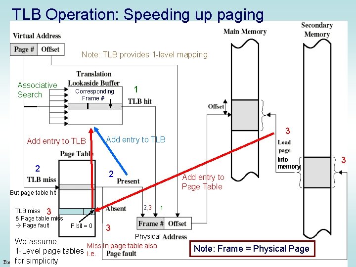
Speeding Up the Paging Mechanism • Paging requires accessing the page table directory and a page table (in main memory) to generate the physical memory address of the required memory location • This slows down memory access • To speed this up, a fast associative mapping cache memory is used to store the most recent page address translations, which are also likely to be accessed in the near future • The 80386 uses a 32 -entry TLB (translation look-aside buffer) for holding the physical addresses of the most recently used 32 memory pages (Translation = mapping from logical to physical). Scenarios: – 1. Hit in the TLB cache? : Very well!, use the address translation in TLB – Miss in the TLB? : • 2. Hit in the page tables: Get translation from page tables in memory and place it in TLB (e. g. by replacing the least-recently-used existing entry there) • 3. Miss in the page tables (page fault), Bring page from mass storage into physical memory and update both the page tables and the TLB Brey: The Intel Microprocessors, 7 e © 2006 Pearson Education, Upper Saddle River, NJ 07458. All Rights Reserved.

TLB Operation: Speeding up paging Note: TLB provides 1 -level mapping Associative Search Corresponding Frame # Add entry to TLB 2 1 Add entry to TLB into memory 2 2, 3 P bit = 0 3 3 Add entry to Page Table But page table hit TLB miss 3 & Page table miss Page fault 3 1 Physical We assume Miss in page table also 1 -Level page tables i. e. Brey: for The simplicity Intel Microprocessors, 7 e Note: Frame = Physical Page © 2006 Pearson Education, Upper Saddle River, NJ 07458. All Rights Reserved.

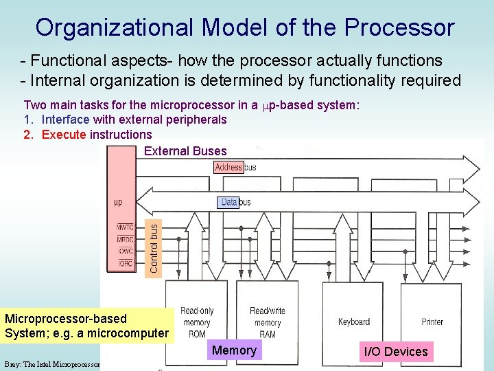
Organizational Model of the Processor - Functional aspects- how the processor actually functions - Internal organization is determined by functionality required Control bus Two main tasks for the microprocessor in a mp-based system: 1. Interface with external peripherals 2. Execute instructions External Buses Microprocessor-based System; e. g. a microcomputer Memory Brey: The Intel Microprocessors, 7 e I/O Devices © 2006 Pearson Education, Upper Saddle River, NJ 07458. All Rights Reserved.

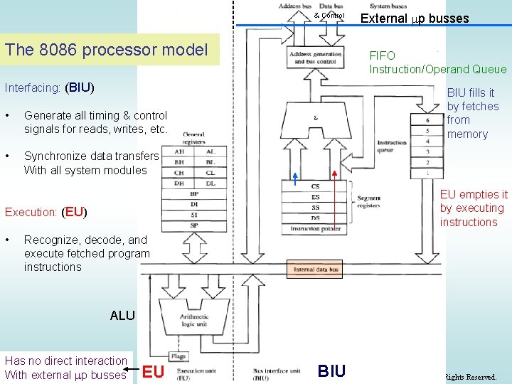
The 8086 processor model (Organization) • Early pipelining attempts • Two main functional units: - The Bus Interface Unit (BIU) - The Execution Unit (EU) • The BIU generates memory and I/O addresses for reading code and transferring data to/from the processor • The EU receives code and data from the BIU, executes the instructions, and stores results in the general purpose registers • Pipelined architecture: Two, hopefully independent operations, are executed at the same time by two separate units: - Fetch by the BIU - Execute by the EU Brey: The Intel Microprocessors, 7 e © 2006 Pearson Education, Upper Saddle River, NJ 07458. All Rights Reserved.

& Control The 8086 processor model FIFO Instruction/Operand Queue Interfacing: (BIU) • Generate all timing & control signals for reads, writes, etc. • Synchronize data transfers With all system modules BIU fills it by fetches from memory EU empties it by executing instructions Execution: (EU) • External mp busses Recognize, decode, and execute fetched program instructions ALU Has no direct interaction With. Theexternal mp busses Brey: Intel Microprocessors, 7 e EU BIU © 2006 Pearson Education, Upper Saddle River, NJ 07458. All Rights Reserved.

The 8086 processor model Non-pipelined 2. Fetch operand b. Start fetching at Wasted fetches the correct target after a Jump inst. location Pipelined (8086) 1. Operand Fetch-Execute Overlap not in Queue * = Wasted Fetches and Executes (inefficiency) 3. Execute a. Oops! Turned out to be a Jump instruction! c. Execute at last! RISC & Modern architectures: • Reduce fetches from memory (operate mostly on registers) Common Scenarios that cause pipeline inefficiency: • Speed up memory fetches (cache) • Use small instructions (both in • Operand is not in queue length and in execution time) • Jump or branch instructions Finer pipeline stages (super • Long-executing instructions: pipelined- 486) e. g. 83 clock cycles for execution vs. 4 Multiple pipelines (superscalar- P 5) cycles for a fetch. Predict how the jump will go BIU fills the buffer and waits idly! Brey: The Intel Microprocessors, 7 e © 2006 Pearson Education, Upper Saddle River, NJ 07458. All Rights Reserved. (branch Prediction)

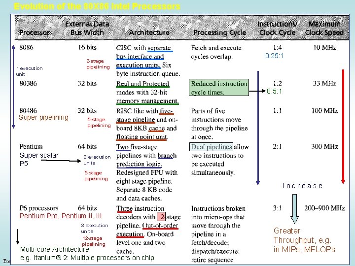
Evolution of the 80 X 86 Intel Processors 1 execution unit 2 -stage pipelining 0. 25: 1 0. 5: 1 Super pipelining Super scalar P 5 5 -stage pipelining 2 execution units 5 -stage pipelining Increase Pentium Pro, Pentium II, III 3 execution units 12 -stage pipelining Multi-core Architecture; e. g. Itanium® 2: Multiple processors on chip Brey: The Intel Microprocessors, 7 e Greater Throughput, e. g. in MIPs, MFLOPs © 2006 Pearson Education, Upper Saddle River, NJ 07458. All Rights Reserved.

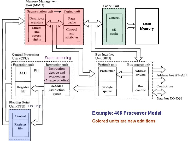
Main Memory Super pipelining EU On Chip Example: 486 Processor Model Colored units are new additions Brey: The Intel Microprocessors, 7 e © 2006 Pearson Education, Upper Saddle River, NJ 07458. All Rights Reserved.

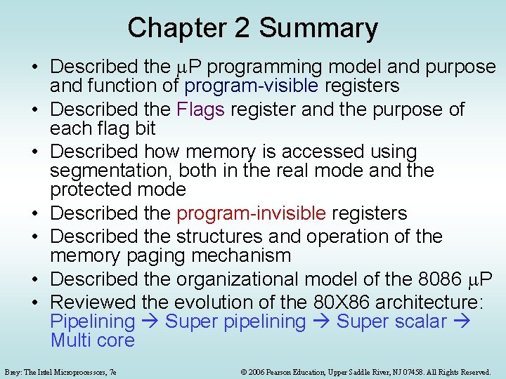
Chapter 2 Summary • Described the m. P programming model and purpose and function of program-visible registers • Described the Flags register and the purpose of each flag bit • Described how memory is accessed using segmentation, both in the real mode and the protected mode • Described the program-invisible registers • Described the structures and operation of the memory paging mechanism • Described the organizational model of the 8086 m. P • Reviewed the evolution of the 80 X 86 architecture: Pipelining Super pipelining Super scalar Multi core Brey: The Intel Microprocessors, 7 e © 2006 Pearson Education, Upper Saddle River, NJ 07458. All Rights Reserved.