Chapter 2 MSP 432 ARM IO Programming 1









- Slides: 59

Chapter 2 MSP 432 ARM I/O Programming 1

Chapter Review • Section 2. 1: MSP 432 Microcontroller and Launch. Pad • Section 2. 2: GPIO (General Purpose I/O) Programming and Interfacing • Section 2. 3: Seven-segment LED interfacing and programming • Section 2. 4: I/O Port Programming in Assembly • Section 2. 5: 16 -BIT I/O ports in MSP 432 • Section 2. 6: Port Mapping Controller 2

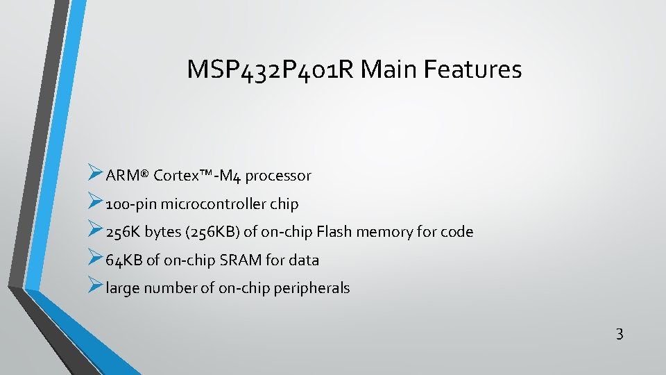
MSP 432 P 401 R Main Features ØARM® Cortex™-M 4 processor Ø 100 -pin microcontroller chip Ø 256 K bytes (256 KB) of on-chip Flash memory for code Ø 64 KB of on-chip SRAM for data Ølarge number of on-chip peripherals 3

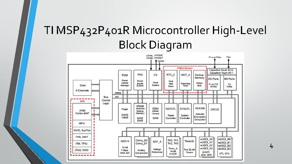
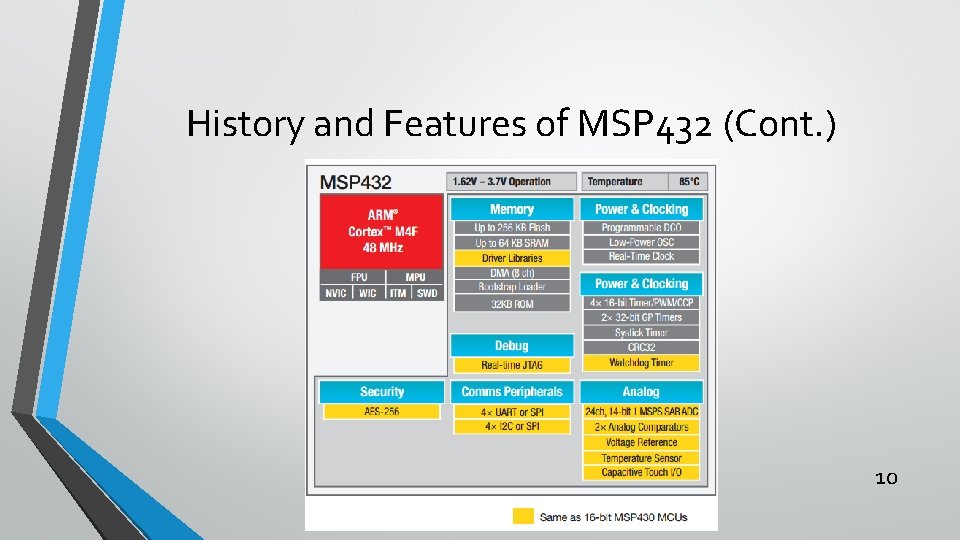
TI MSP 432 P 401 R Microcontroller High-Level Block Diagram 4

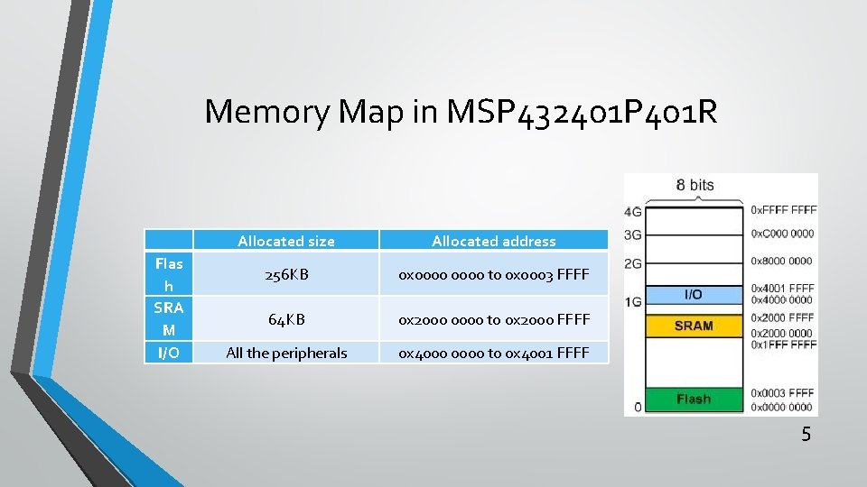
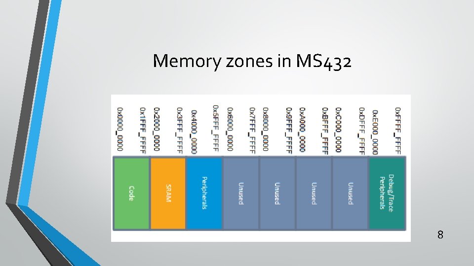
Memory Map in MSP 432401 P 401 R Flas h SRA M I/O Allocated size Allocated address 256 KB 0 x 0000 to 0 x 0003 FFFF 64 KB 0 x 2000 0000 to 0 x 2000 FFFF All the peripherals 0 x 4000 0000 to 0 x 4001 FFFF 5

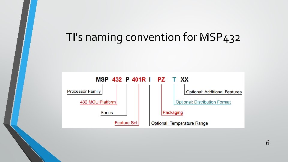
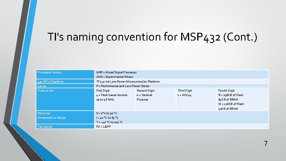
TI's naming convention for MSP 432 6

TI's naming convention for MSP 432 (Cont. ) Processor Family 432 MCU Platform Series Feature Set Optional: Temperature Range Packaging MSP = Mixed Signal Processor XMS = Experimental Silicon TI’s 32 -bit Low-Power Microcontroller Platform P = Performance and Low-Power Series First Digit Second Digit 4 = Flash based devices 0 = General up to 48 MHz Purpose Third Digit 1 = ADC 14 Fourth Digit R = 256 KB of Flash 64 KB of SRAM M = 128 KB of Flash 32 KB of SRAM S = 0°C to 50 °C I = 40 °C to 85 °C T = – 40 °C to 105 °C PZ = LQFP 7

Memory zones in MS 432 8

History and Features of MSP 432 • TI used the venerable 8051 microcontroller for their mixed signal processors • TI came up with MSP 430 chip Due to the need for low power chip and 8051 limitations • MSP stands for Mixed Signal Processor • The MSP 430 is a 16 -bit RISC CPU designed and marketed exclusively by TI • In 2015, TI introduced an ARM-based device to the MSP 430 Family and called it MSP 432 9

History and Features of MSP 432 (Cont. ) 10

Section 2. 2: GPIO (General Purpose I/O) Programming and Interfacing • In the microcontroller, we have two types of I/O: a. General Purpose I/O (GPIO): The GPIO ports are used for interfacing devices such as LEDs, switches, LCD, keypad, and so on. • Special purpose I/O: These I/O ports have designated function such as ADC (Analog-to-Digital), Timer, UART (universal asynchronous receiver transmitter), and so on. 11

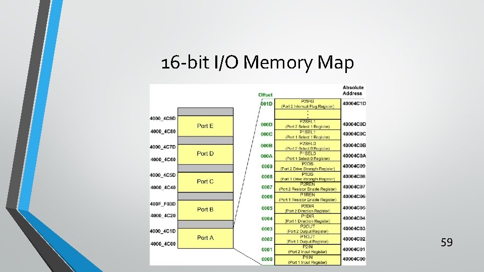
GPIO • The GPIO ports in MSP 432 are designated as port P 1 to P 10 + PJ • P 1 to P 10 are also referred as the Simple I/O or Digital I/O ports • port J has special function such as external crystal oscillator and JTAG connections • The base address of I/O port is 0 x 4000 4 C 00 12

GPIO Offset Addresses § § § § § GPIO P 1 : 0 x 4000 4 C 00 + 0 (even addresses) GPIO P 2 : 0 x 4000 4 C 00 + 1 (odd addresses) GPIO P 3 : 0 x 4000 4 C 00 + 20 (even addresses) GPIO P 4 : 0 x 4000 4 C 00 + 21 (odd addresses) GPIO P 5 : 0 x 4000 4 C 00 + 40 (even addresses) GPIO P 6 : 0 x 4000 4 C 00 + 41 (odd addresses) GPIO P 7 : 0 x 4000 4 C 00 + 60 (even addresses) GPIO P 8 : 0 x 4000 4 C 00 + 61 (odd addresses) GPIO P 9 : 0 x 4000 4 C 00 + 80 (even addresses) GPIO P 10 : 0 x 4000 4 C 00 + 81 (odd addresses) 13

I/O Pins in MSP 432 Launch. Pad board • I/O ports are named with numbers P 1, P 2, P 3, and so on • The pins are designated as P 1. 0 -P 1. 7, P 2. 0 -P 2. 7, P 3. 0 -P 3. 7, and so on • The MSP 432 P 401 R has Ports P 0, P 1, P 2, P 3, P 4, P 5, P 6, P 7, P 8, P 9, P 10 and PJ • P 10 and PJ have only 6 pins while all other ports have 8 pins • we can combine two 8 -bit ports to come up with 16 -bit port 14

MSP 432 P 401 R 100 -pin package pin-out 15

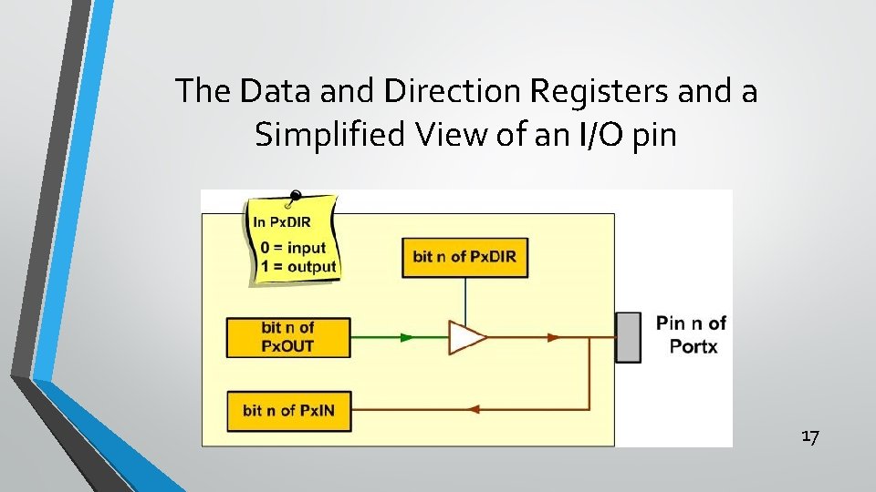
Direction and Data Registers • Generally every microcontroller has minimum of three registers associated with each of GPIO port • Data IN, Data Out, and Direction • The Direction register is used to make the pin either input or output • we use the Data register to actually write to the pin (Px. OUT) or read data from the pin (Px. IN) 16

The Data and Direction Registers and a Simplified View of an I/O pin 17

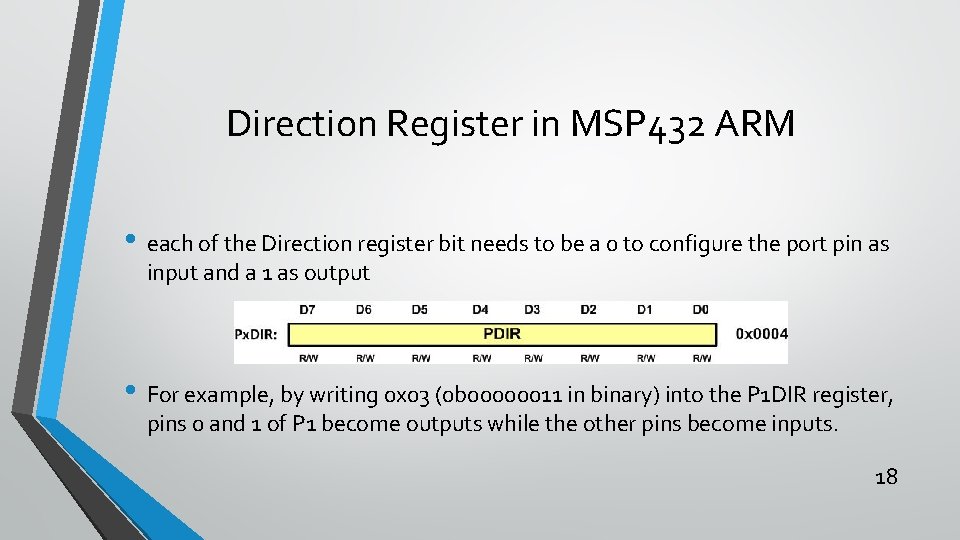
Direction Register in MSP 432 ARM • each of the Direction register bit needs to be a 0 to configure the port pin as input and a 1 as output • For example, by writing 0 x 03 (0 b 00000011 in binary) into the P 1 DIR register, pins 0 and 1 of P 1 become outputs while the other pins become inputs. 18

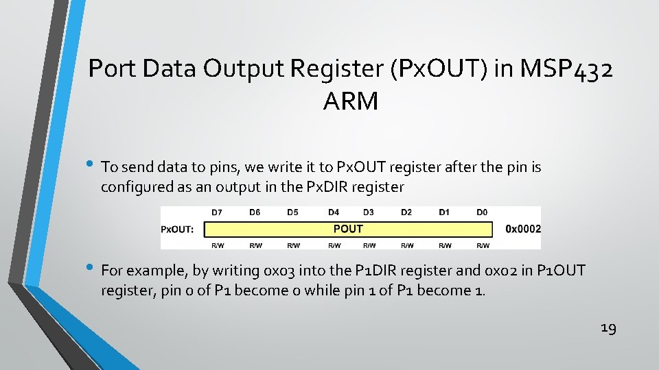
Port Data Output Register (Px. OUT) in MSP 432 ARM • To send data to pins, we write it to Px. OUT register after the pin is configured as an output in the Px. DIR register • For example, by writing 0 x 03 into the P 1 DIR register and 0 x 02 in P 1 OUT register, pin 0 of P 1 become 0 while pin 1 of P 1 become 1. 19

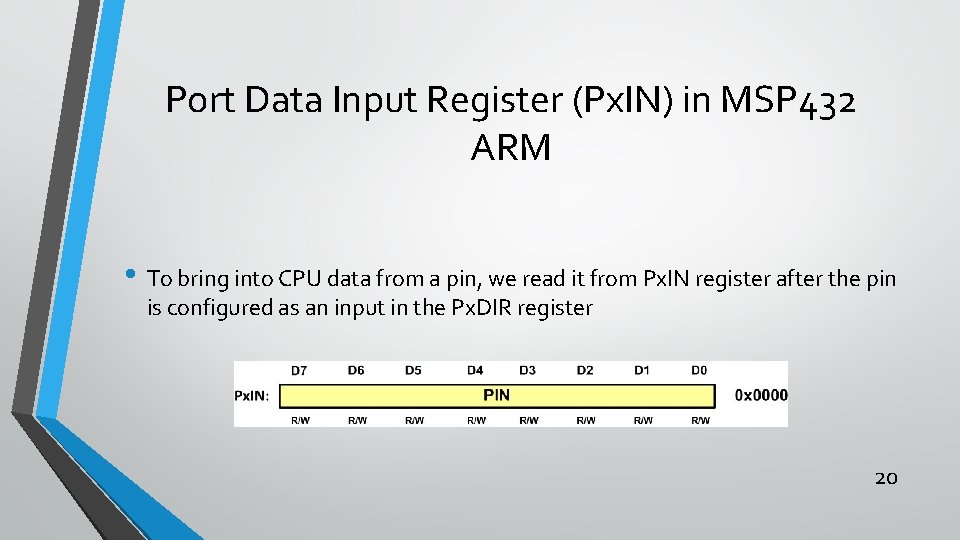
Port Data Input Register (Px. IN) in MSP 432 ARM • To bring into CPU data from a pin, we read it from Px. IN register after the pin is configured as an input in the Px. DIR register 20

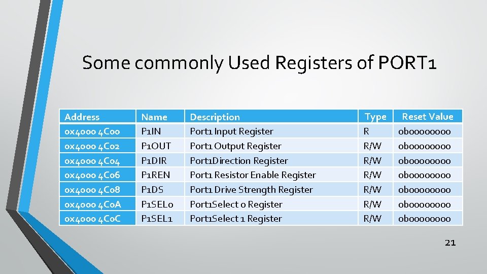
Some commonly Used Registers of PORT 1 Address 0 x 4000 4 C 00 0 x 4000 4 C 02 0 x 4000 4 C 04 0 x 4000 4 C 06 0 x 4000 4 C 08 0 x 4000 4 C 0 A 0 x 4000 4 C 0 C Name P 1 IN P 1 OUT P 1 DIR P 1 REN P 1 DS P 1 SEL 0 P 1 SEL 1 Description Port 1 Input Register Port 1 Output Register Port 1 Direction Register Port 1 Resistor Enable Register Port 1 Drive Strength Register Port 1 Select 0 Register Port 1 Select 1 Register Type R R/W R/W R/W Reset Value 0 b 00000000 0 b 00000000 0 b 0000 21

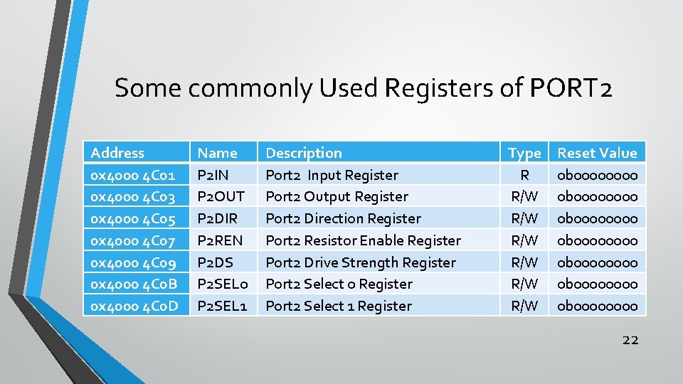
Some commonly Used Registers of PORT 2 Address 0 x 4000 4 C 01 0 x 4000 4 C 03 0 x 4000 4 C 05 0 x 4000 4 C 07 0 x 4000 4 C 09 0 x 4000 4 C 0 B 0 x 4000 4 C 0 D Name P 2 IN P 2 OUT P 2 DIR P 2 REN P 2 DS P 2 SEL 0 P 2 SEL 1 Description Port 2 Input Register Port 2 Output Register Port 2 Direction Register Port 2 Resistor Enable Register Port 2 Drive Strength Register Port 2 Select 0 Register Port 2 Select 1 Register Type R R/W R/W R/W Reset Value 0 b 00000000 0 b 00000000 0 b 0000 22

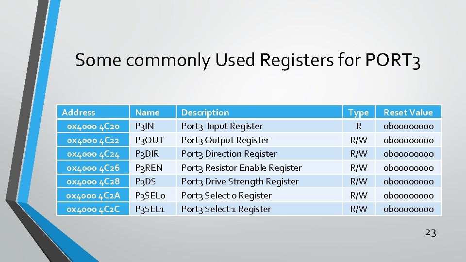
Some commonly Used Registers for PORT 3 Address 0 x 4000 4 C 20 0 x 4000 4 C 22 0 x 4000 4 C 24 0 x 4000 4 C 26 0 x 4000 4 C 28 0 x 4000 4 C 2 A 0 x 4000 4 C 2 C Name P 3 IN P 3 OUT P 3 DIR P 3 REN P 3 DS P 3 SEL 0 P 3 SEL 1 Description Port 3 Input Register Port 3 Output Register Port 3 Direction Register Port 3 Resistor Enable Register Port 3 Drive Strength Register Port 3 Select 0 Register Port 3 Select 1 Register Type R R/W R/W R/W Reset Value 0 b 00000000 0 b 00000000 0 b 0000 23

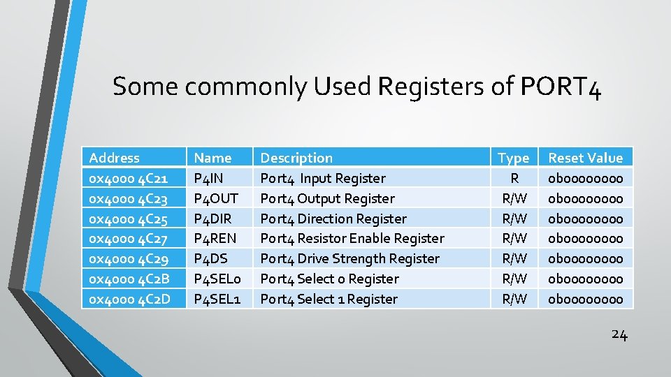
Some commonly Used Registers of PORT 4 Address 0 x 4000 4 C 21 0 x 4000 4 C 23 0 x 4000 4 C 25 0 x 4000 4 C 27 0 x 4000 4 C 29 0 x 4000 4 C 2 B 0 x 4000 4 C 2 D Name P 4 IN P 4 OUT P 4 DIR P 4 REN P 4 DS P 4 SEL 0 P 4 SEL 1 Description Port 4 Input Register Port 4 Output Register Port 4 Direction Register Port 4 Resistor Enable Register Port 4 Drive Strength Register Port 4 Select 0 Register Port 4 Select 1 Register Type R R/W R/W R/W Reset Value 0 b 00000000 0 b 00000000 0 b 0000 24

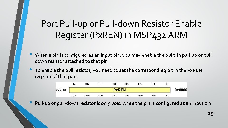
Port Pull-up or Pull-down Resistor Enable Register (Px. REN) in MSP 432 ARM • When a pin is configured as an input pin, you may enable the built-in pull-up or pulldown resistor attached to that pin • To enable the pull resistor, you need to set the corresponding bit in the Px. REN register of that port • Pull-up or pull-down resistor is only used when the pin is configured as an input pin 25

Example • Find the value for P 2 DIR, P 2 OUT, and P 2 REN to configure the P 2 pins as inputs. Pull down P 2. 0 and pull up P 2. 1. • Solution: P 2 DIR = 0 b 0000 = 0 x 00 P 2 REN = 0 b 00000011 = 0 x 03 P 2 OUT = 0 b 00000010 = 0 x 02 26

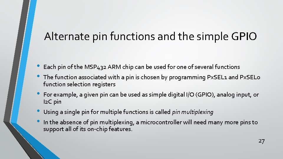
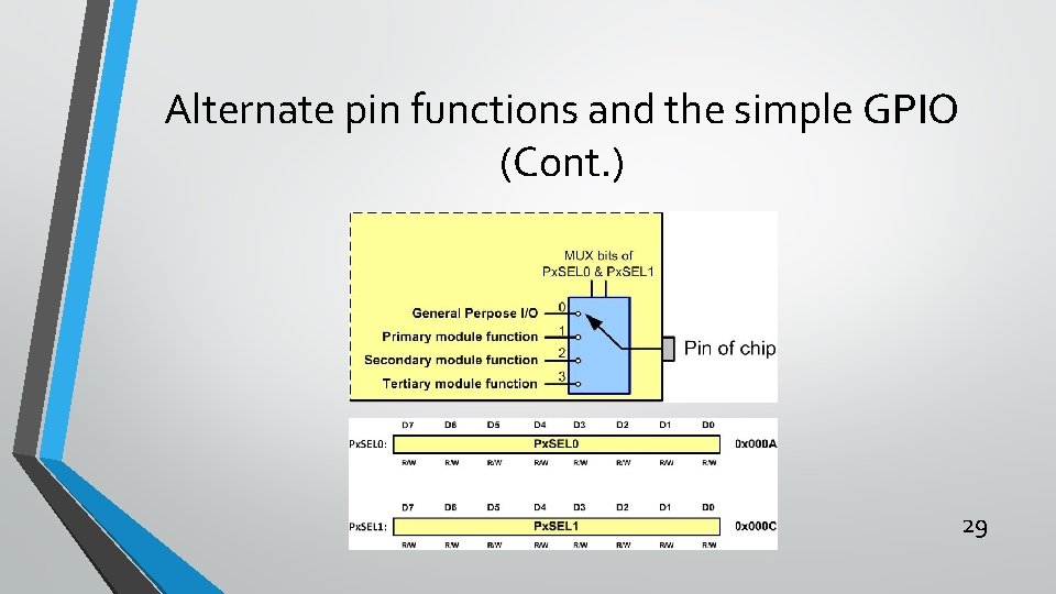
Alternate pin functions and the simple GPIO • • Each pin of the MSP 432 ARM chip can be used for one of several functions • For example, a given pin can be used as simple digital I/O (GPIO), analog input, or I 2 C pin • • The function associated with a pin is chosen by programming Px. SEL 1 and Px. SEL 0 function selection registers Using a single pin for multiple functions is called pin multiplexing In the absence of pin multiplexing, a microcontroller will need many more pins to support all of its on-chip features. 27

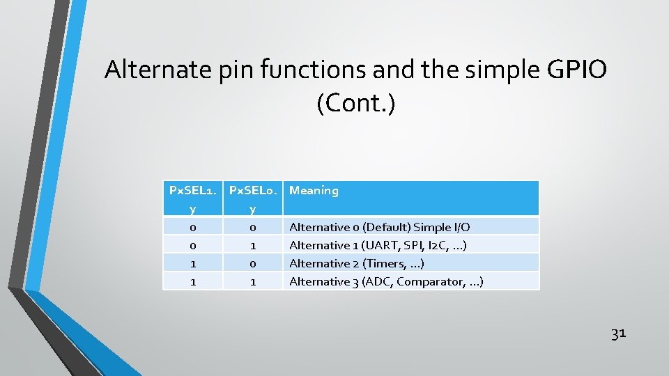
Alternate pin functions and the simple GPIO (Cont. ) • The Px. SEL 1 and Px. SEL 0 (Portx Selection 1 and 0 function selection) registers allow us to program a pin to be used for a given alternate function • Upon reset, ports 1 to 10 are configured for simple I/O. At any given situation • To use a pin as simple digital I/O, we must choose Px. SEL 1: Px. SEL 0=00 option 28

Alternate pin functions and the simple GPIO (Cont. ) 29

Alternate pin functions and the simple GPIO (Cont. ) • Upon power-on reset, the default selection is Simple I/O (Px. SEL 1: PXSEL 0 = 00) for all pins • For option Px. SEL 1: PXSEL 0 = 01, the pins may have alternate functions of UART, SPI, and I 2 C, timers, and so on • For option 2, some of the alternate functions are associated with timers • The analog functions ADC and comparators use alternate function 3 30

Alternate pin functions and the simple GPIO (Cont. ) Px. SEL 1. Px. SEL 0. Meaning y y 0 0 Alternative 0 (Default) Simple I/O 0 1 Alternative 1 (UART, SPI, I 2 C, …) 1 0 Alternative 2 (Timers, …) 1 1 Alternative 3 (ADC, Comparator, …) 31

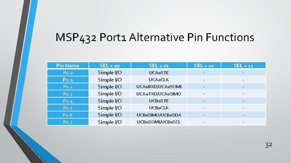
MSP 432 Port 1 Alternative Pin Functions Pin Name P 1. 0 P 1. 1 P 1. 2 P 1. 3 P 1. 4 P 1. 5 P 1. 6 P 1. 7 SEL = 00 Simple I/O Simple I/O SEL = 01 UCA 0 STE UCA 0 CLK UCA 0 RXD/UCA 0 SOMI UCA 0 TXD/UCA 0 SIMO UCB 0 STE UCB 0 CLK UCB 0 SIMO/UCB 0 SDA UCB 0 SOMI/UCB 0 SCL SEL = 10 - SEL = 11 - 32

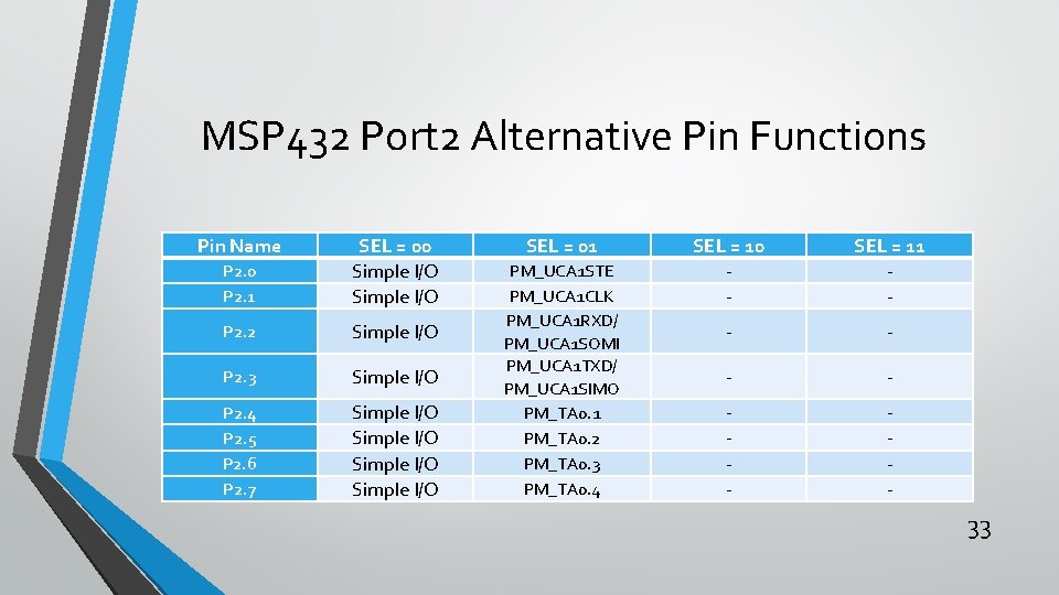
MSP 432 Port 2 Alternative Pin Functions Pin Name P 2. 0 P 2. 1 SEL = 00 Simple I/O P 2. 2 Simple I/O P 2. 3 Simple I/O P 2. 4 P 2. 5 P 2. 6 P 2. 7 Simple I/O SEL = 01 PM_UCA 1 STE PM_UCA 1 CLK PM_UCA 1 RXD/ PM_UCA 1 SOMI PM_UCA 1 TXD/ PM_UCA 1 SIMO PM_TA 0. 1 PM_TA 0. 2 PM_TA 0. 3 PM_TA 0. 4 SEL = 10 - SEL = 11 - - - - 33

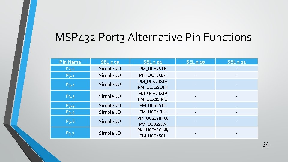
MSP 432 Port 3 Alternative Pin Functions Pin Name P 3. 0 P 3. 1 SEL = 00 Simple I/O P 3. 2 Simple I/O P 3. 3 Simple I/O P 3. 4 P 3. 5 Simple I/O P 3. 6 Simple I/O P 3. 7 Simple I/O SEL = 01 PM_UCA 2 STE PM_UCA 2 CLK PM_UCA 2 RXD/ PM_UCA 2 SOMI PM_UCA 2 TXD/ PM_UCA 2 SIMO PM_UCB 2 STE PM_UCB 2 CLK PM_UCB 2 SIMO/ PM_UCB 2 SDA PM_UCB 2 SOMI/ PM_UCB 2 SCL SEL = 10 - SEL = 11 - - - 34

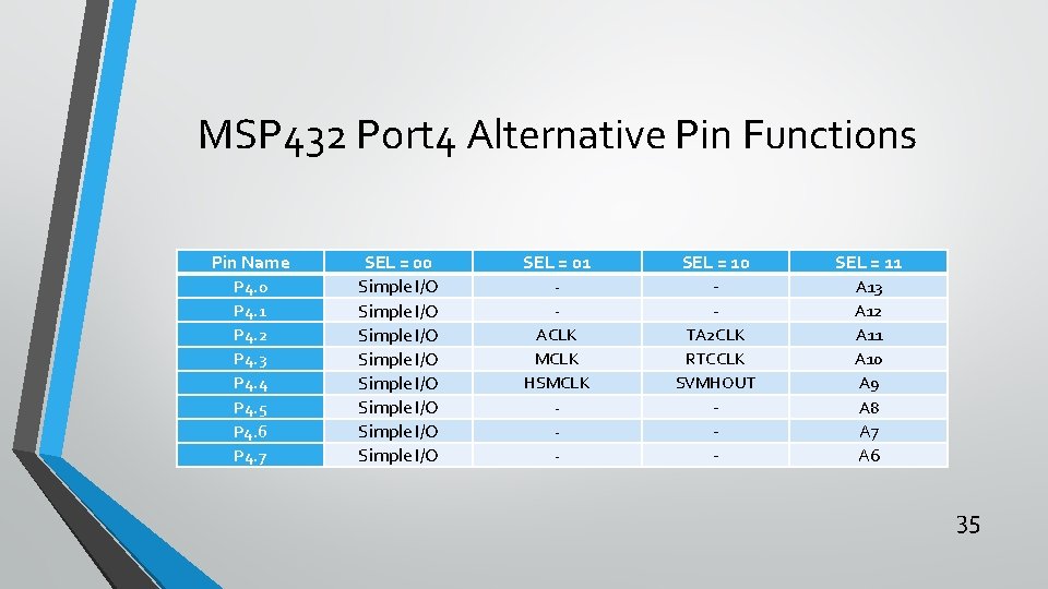
MSP 432 Port 4 Alternative Pin Functions Pin Name P 4. 0 P 4. 1 P 4. 2 P 4. 3 P 4. 4 P 4. 5 P 4. 6 P 4. 7 SEL = 00 Simple I/O Simple I/O SEL = 01 ACLK MCLK HSMCLK - SEL = 10 TA 2 CLK RTCCLK SVMHOUT - SEL = 11 A 13 A 12 A 11 A 10 A 9 A 8 A 7 A 6 35

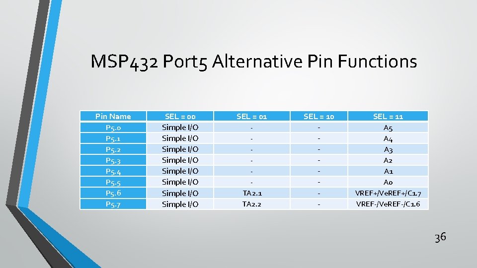
MSP 432 Port 5 Alternative Pin Functions Pin Name P 5. 0 P 5. 1 P 5. 2 P 5. 3 P 5. 4 P 5. 5 P 5. 6 P 5. 7 SEL = 00 Simple I/O Simple I/O SEL = 01 TA 2. 2 SEL = 10 - SEL = 11 A 5 A 4 A 3 A 2 A 1 A 0 VREF+/Ve. REF+/C 1. 7 VREF-/Ve. REF-/C 1. 6 36

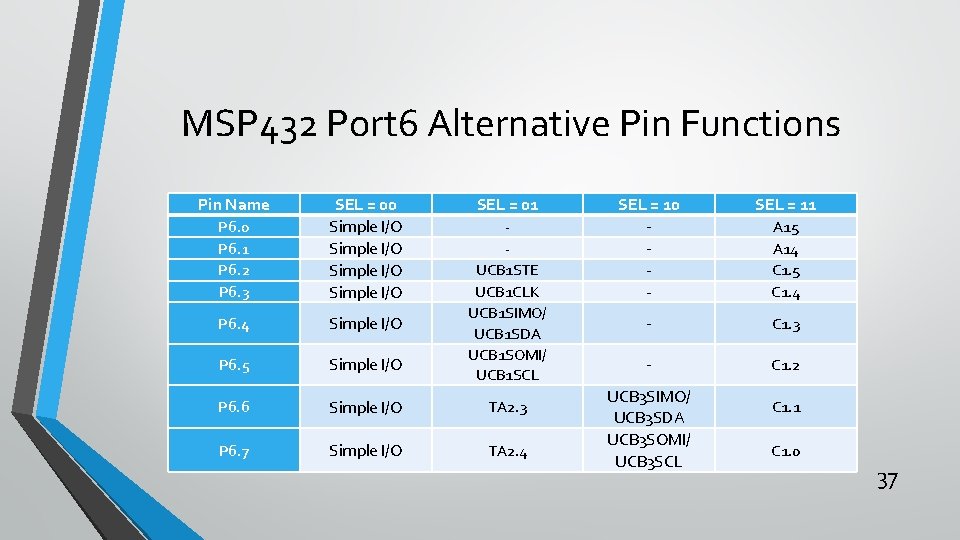
MSP 432 Port 6 Alternative Pin Functions Pin Name P 6. 0 P 6. 1 P 6. 2 P 6. 3 SEL = 00 Simple I/O SEL = 01 P 6. 4 Simple I/O P 6. 5 Simple I/O P 6. 6 Simple I/O TA 2. 3 P 6. 7 Simple I/O TA 2. 4 UCB 1 STE UCB 1 CLK UCB 1 SIMO/ UCB 1 SDA UCB 1 SOMI/ UCB 1 SCL SEL = 10 - SEL = 11 - C 1. 3 - C 1. 2 UCB 3 SIMO/ UCB 3 SDA UCB 3 SOMI/ UCB 3 SCL A 15 A 14 C 1. 5 C 1. 4 C 1. 1 C 1. 0 37

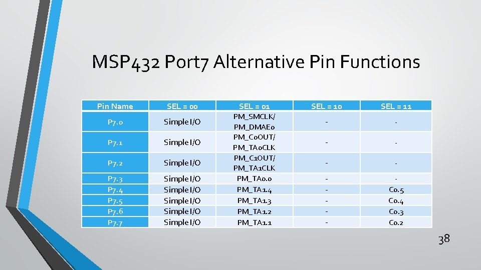
MSP 432 Port 7 Alternative Pin Functions Pin Name SEL = 00 P 7. 0 Simple I/O P 7. 1 Simple I/O P 7. 2 Simple I/O P 7. 3 P 7. 4 P 7. 5 P 7. 6 P 7. 7 Simple I/O Simple I/O SEL = 01 PM_SMCLK/ PM_DMAE 0 PM_C 0 OUT/ PM_TA 0 CLK PM_C 1 OUT/ PM_TA 1 CLK PM_TA 0. 0 PM_TA 1. 4 PM_TA 1. 3 PM_TA 1. 2 PM_TA 1. 1 SEL = 10 SEL = 11 - - - - C 0. 5 C 0. 4 C 0. 3 C 0. 2 38

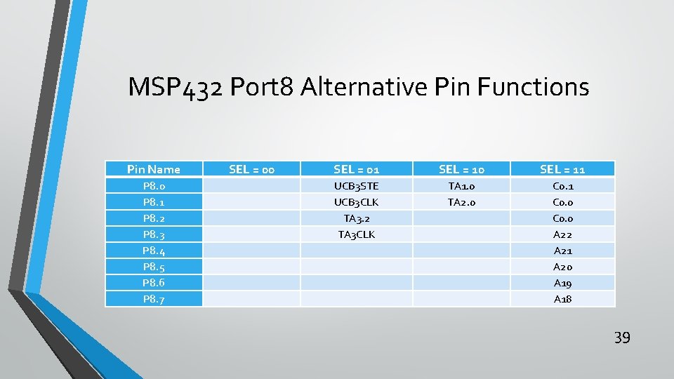
MSP 432 Port 8 Alternative Pin Functions Pin Name P 8. 0 P 8. 1 P 8. 2 P 8. 3 P 8. 4 P 8. 5 P 8. 6 P 8. 7 SEL = 00 SEL = 01 SEL = 10 SEL = 11 UCB 3 STE UCB 3 CLK TA 3. 2 TA 3 CLK TA 1. 0 TA 2. 0 C 0. 1 C 0. 0 A 22 A 21 A 20 A 19 A 18 39

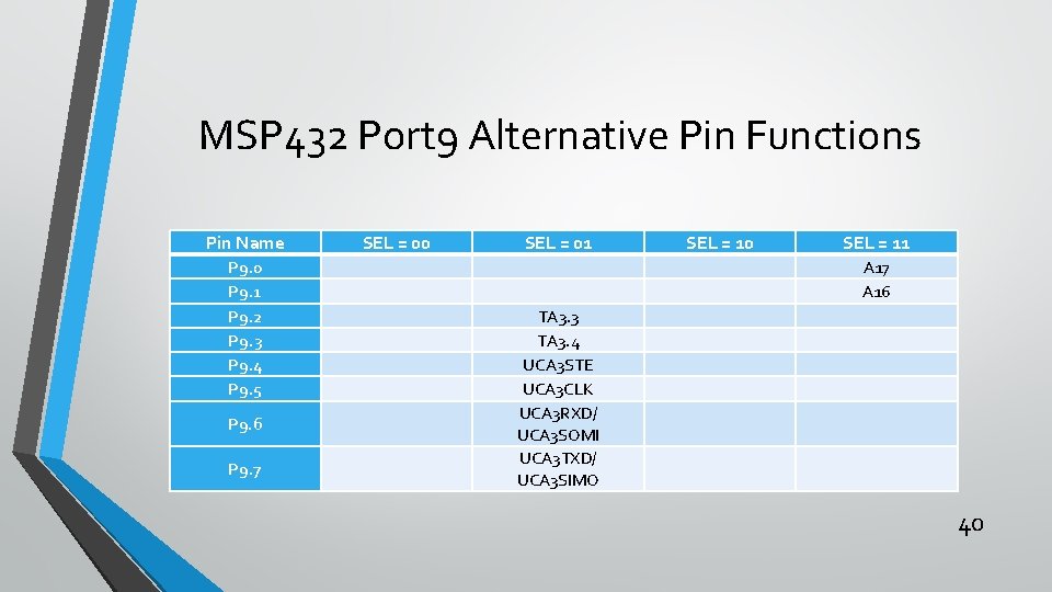
MSP 432 Port 9 Alternative Pin Functions Pin Name P 9. 0 P 9. 1 P 9. 2 P 9. 3 P 9. 4 P 9. 5 SEL = 00 P 9. 6 P 9. 7 SEL = 01 SEL = 10 SEL = 11 TA 3. 3 TA 3. 4 UCA 3 STE UCA 3 CLK UCA 3 RXD/ UCA 3 SOMI UCA 3 TXD/ UCA 3 SIMO A 17 A 16 40

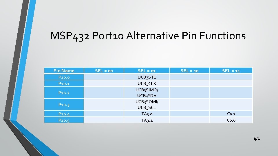
MSP 432 Port 10 Alternative Pin Functions Pin Name P 10. 0 P 10. 1 SEL = 00 P 10. 2 P 10. 3 P 10. 4 P 10. 5 SEL = 01 SEL = 10 SEL = 11 UCB 3 STE UCB 3 CLK UCB 3 SIMO/ UCB 3 SDA UCB 3 SOMI/ UCB 3 SCL TA 3. 0 TA 3. 1 C 0. 7 C 0. 6 41

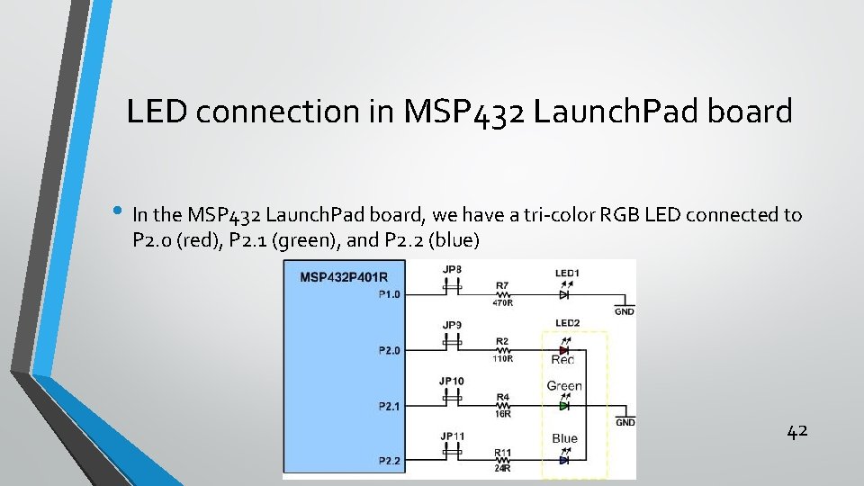
LED connection in MSP 432 Launch. Pad board • In the MSP 432 Launch. Pad board, we have a tri-color RGB LED connected to P 2. 0 (red), P 2. 1 (green), and P 2. 2 (blue) 42

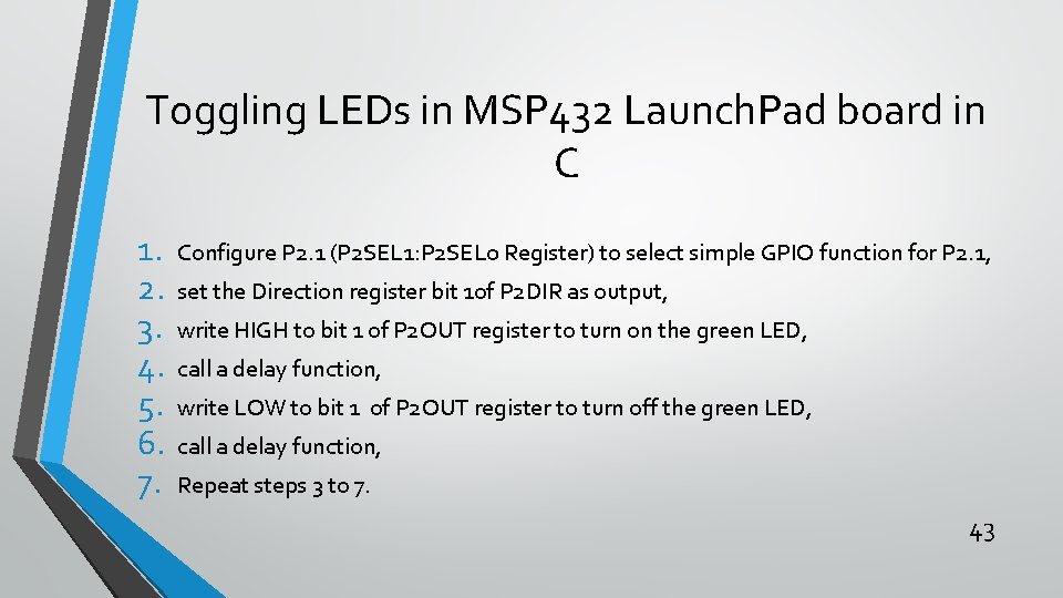
Toggling LEDs in MSP 432 Launch. Pad board in C 1. 2. 3. 4. 5. 6. 7. Configure P 2. 1 (P 2 SEL 1: P 2 SEL 0 Register) to select simple GPIO function for P 2. 1, set the Direction register bit 1 of P 2 DIR as output, write HIGH to bit 1 of P 2 OUT register to turn on the green LED, call a delay function, write LOW to bit 1 of P 2 OUT register to turn off the green LED, call a delay function, Repeat steps 3 to 7. 43

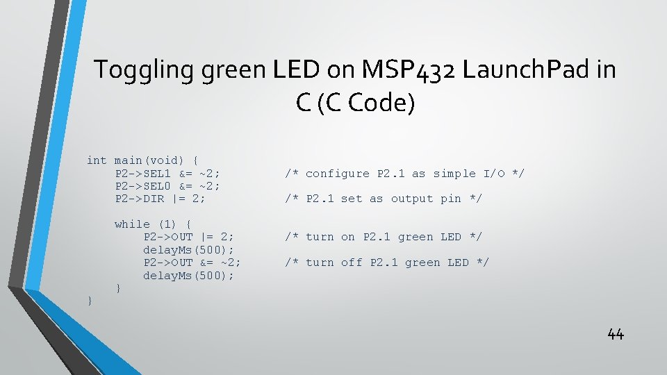
Toggling green LED on MSP 432 Launch. Pad in C (C Code) int main(void) { P 2 ->SEL 1 &= ~2; /* configure P 2. 1 as simple I/O */ P 2 ->SEL 0 &= ~2; P 2 ->DIR |= 2; /* P 2. 1 set as output pin */ while (1) { P 2 ->OUT |= 2; /* turn on P 2. 1 green LED */ delay. Ms(500); P 2 ->OUT &= ~2; /* turn off P 2. 1 green LED */ delay. Ms(500); } } 44

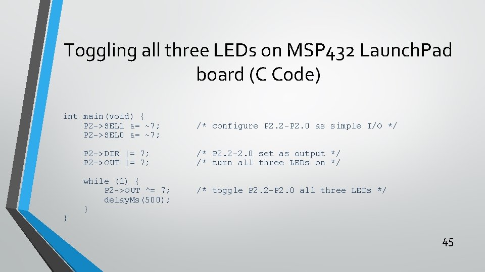
Toggling all three LEDs on MSP 432 Launch. Pad board (C Code) int main(void) { P 2 ->SEL 1 &= ~7; /* configure P 2. 2 -P 2. 0 as simple I/O */ P 2 ->SEL 0 &= ~7; P 2 ->DIR |= 7; /* P 2. 2 -2. 0 set as output */ P 2 ->OUT |= 7; /* turn all three LEDs on */ while (1) { P 2 ->OUT ^= 7; /* toggle P 2. 2 -P 2. 0 all three LEDs */ delay. Ms(500); } } 45

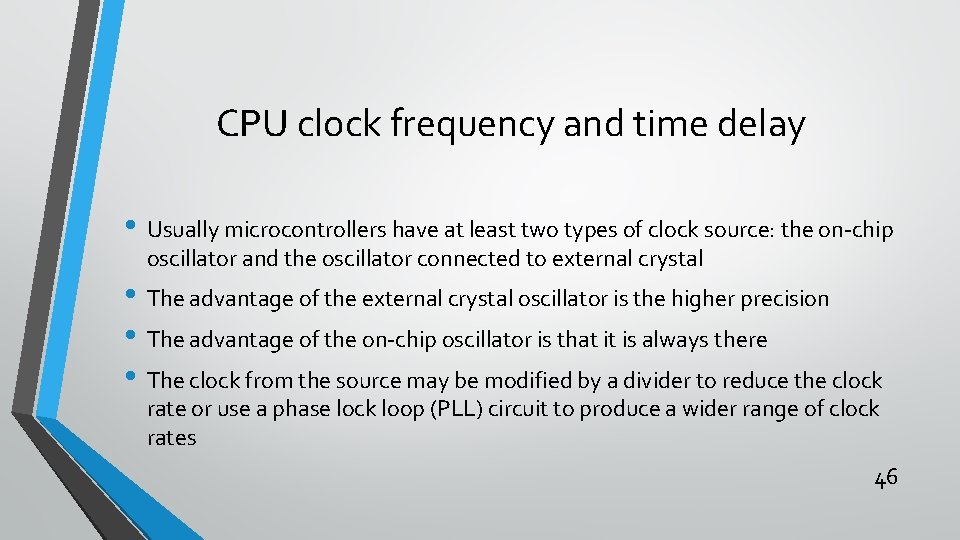
CPU clock frequency and time delay • Usually microcontrollers have at least two types of clock source: the on-chip oscillator and the oscillator connected to external crystal • The advantage of the external crystal oscillator is the higher precision • The advantage of the on-chip oscillator is that it is always there • The clock from the source may be modified by a divider to reduce the clock rate or use a phase lock loop (PLL) circuit to produce a wider range of clock rates 46

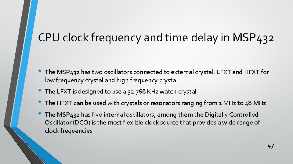
CPU clock frequency and time delay in MSP 432 • The MSP 432 has two oscillators connected to external crystal, LFXT and HFXT for low frequency crystal and high frequency crystal • • • The LFXT is designed to use a 32. 768 KHz watch crystal The HFXT can be used with crystals or resonators ranging from 1 MHz to 48 MHz The MSP 432 has five internal oscillators, among them the Digitally Controlled Oscillator (DCO) is the most flexible clock source that provides a wide range of clock frequencies 47

Measuring time delay in a C program loop • One simple way of creating a time delay is using a for-loop in C language • The length of time delay loop for a given system is function of two factors: a) the CPU frequency and b) the compiler • Regardless of clock source to CPU and the C compiler used, always use oscilloscope to measure the length of time delay loop for a given system with a given compiler and compiler option setting 48

Connecting switches to MSP 432 49

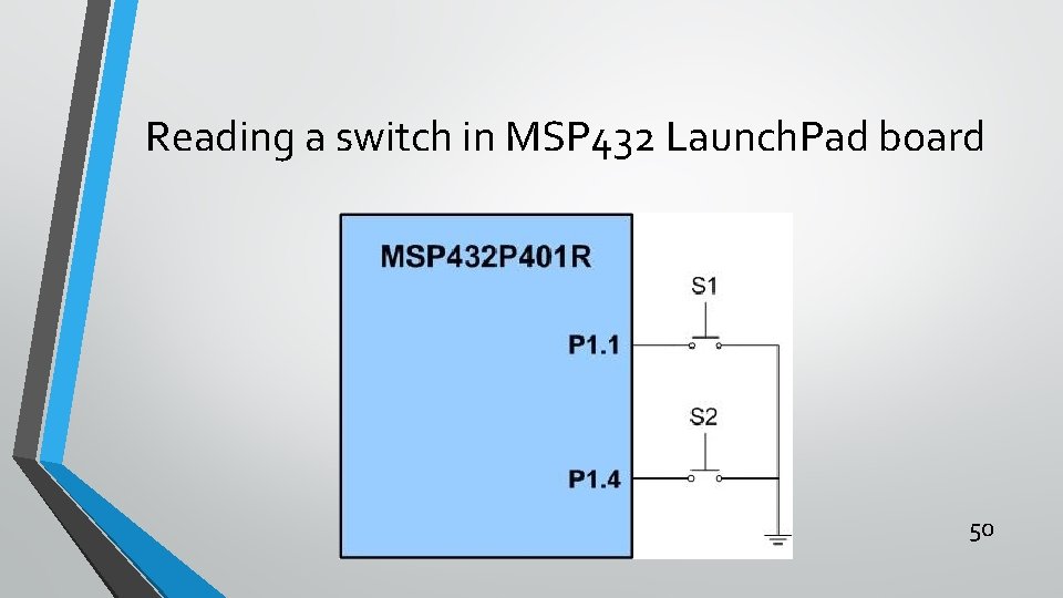
Reading a switch in MSP 432 Launch. Pad board 50

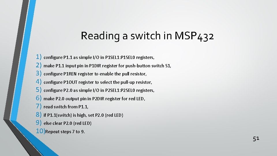
Reading a switch in MSP 432 1) configure P 1. 1 as simple I/O in P 1 SEL 1: P 1 SEL 0 registers, 2) make P 1. 1 input pin in P 1 DIR register for push-button switch S 1, 3) configure P 1 REN register to enable the pull resistor, 4) configure P 1 OUT register to select the pull-up resistor, 5) configure P 2. 0 as simple I/O in P 2 SEL 1: P 2 SEL 0 registers, 6) make P 2. 0 output pin in P 2 DIR register for red LED, 7) read switch from P 1. 1, 8) if P 1. 1(switch) is high, set P 2. 0 (red LED) 9) else clear P 2. 0 (red LED) 10)Repeat steps 7 to 9. 51

Reading a switch and displaying it on LED int main(void) { P 1 ->SEL 1 &= ~2; /* configure P 1. 1 as simple I/O */ P 1 ->SEL 0 &= ~2; P 1 ->DIR &= ~2; /* P 1. 1 set as input */ P 1 ->REN |= 2; /* P 1. 1 pull resistor enabled */ P 1 ->OUT |= 2; /* Pull up/down is selected by P 1 ->OUT */ P 2 ->SEL 1 &= ~1; /* configure P 2. 0 as simple I/O */ P 2 ->SEL 0 &= ~1; P 2 ->DIR |= 1; /* P 2. 0 set as output pin */ while (1) { if (P 1 ->IN & 2) /* use switch 1 to control red LED */ P 2 ->OUT &= ~1; /* turn off P 2. 0 red LED when SW is not pressed */ else P 2 ->OUT |= 1; /* turn on P 2. 0 red LED when SW is pressed */ } } 52

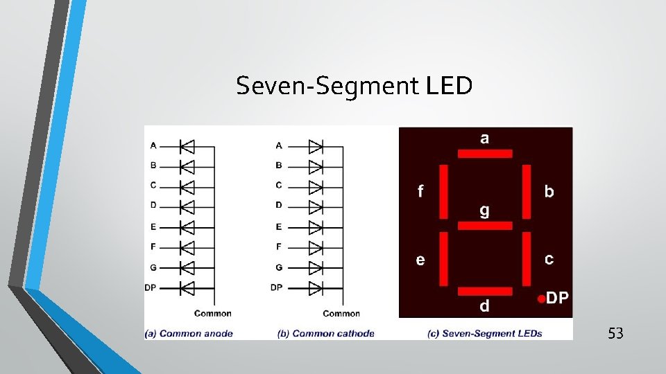
Seven-Segment LED 53

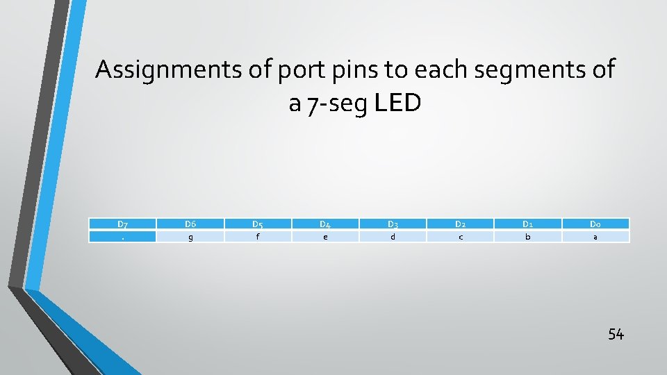
Assignments of port pins to each segments of a 7 -seg LED D 7. D 6 g D 5 f D 4 e D 3 d D 2 c D 1 b D 0 a 54

Segment patterns for the 10 decimal digits for a common cathode 7 -seg LED Num 0 1 2 3 4 5 6 7 8 9 D 7. 0 0 0 0 0 D 6 g 0 0 1 1 1 0 1 1 D 5 f 1 0 0 0 1 1 1 0 1 1 D 4 e 1 0 0 0 1 0 D 3 d 1 0 1 1 D 2 c 1 1 0 1 1 1 1 D 1 b 1 1 1 0 0 1 1 1 D 0 a 1 0 1 1 1 Hex value 0 x 3 F 0 x 06 0 x 5 B 0 x 4 F 0 x 66 0 x 6 D 0 x 7 D 0 x 07 0 x 7 F 0 x 6 F 55

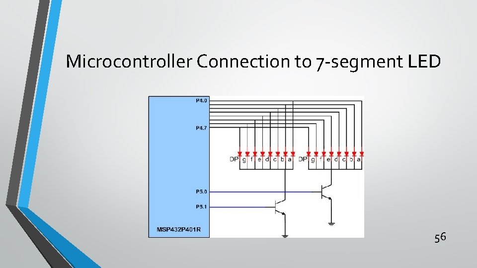
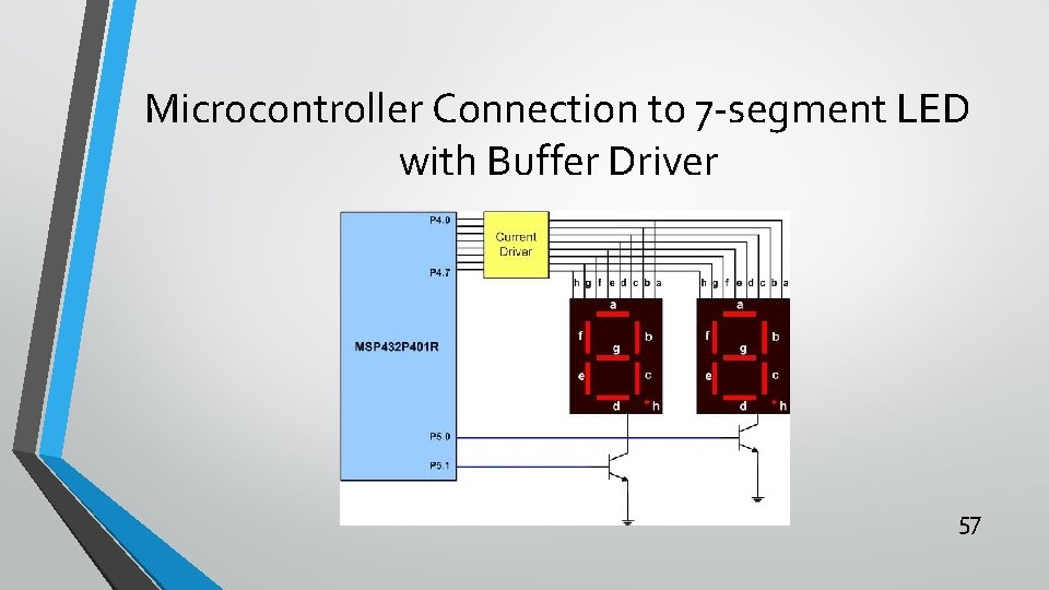
Microcontroller Connection to 7 -segment LED 56

Microcontroller Connection to 7 -segment LED with Buffer Driver 57

Seven-segment LED interfacing and programming if we want to display number 75 on the 7 -seg LED, the following steps should be used: 1) Configure Port 4 as output port to drive the segments, 2) Configure Port 5 as output port to select the digits, 3) Write the pattern of numeral 7 from Table 2 10 to Port 4, 4) Clear the P 5. 0 pin to turn off the ones digit, 5) Set the P 5. 1 pin HIGH to activate the tens digit, 6) Delay for some time, 7) Write the pattern of numeral 5 from Table 2 10 to Port 4, 8) Clear the P 5. 1 pin to turn off the tens digit, 9) Set the P 5. 0 pin HIGH to activate the ones digit, 10) Delay for some time, 11) Repeat from step 3 to 11. 58

16 -bit I/O Memory Map 59