Chapter 2 Manufacturing Process and CMOS Circuit Layout




- Slides: 47

Chapter 2 Manufacturing Process and CMOS Circuit Layout 1 st rev. : March 7, 2003 2 nd rev. : April 10, 2003 1 EE 141 Manufacturing

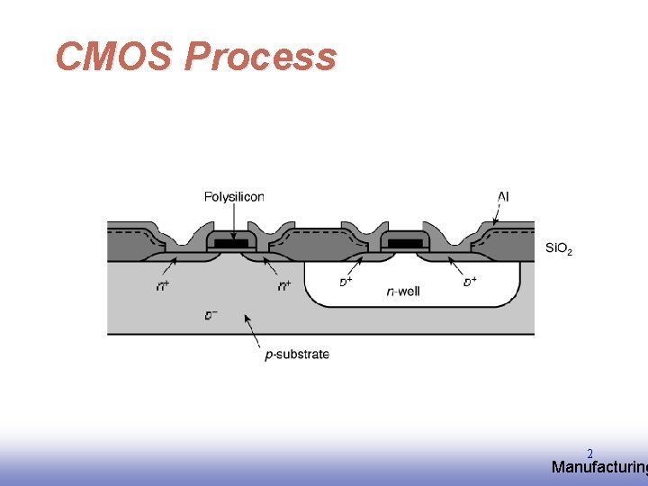
CMOS Process 2 EE 141 Manufacturing

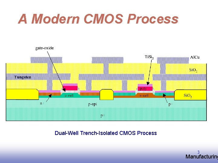
A Modern CMOS Process Dual-Well Trench-Isolated CMOS Process 3 EE 141 Manufacturing

The Manufacturing Process For a great tour through the IC manufacturing process and its different steps, check www. fullman. com/semiconductors. html 4 EE 141 Manufacturing

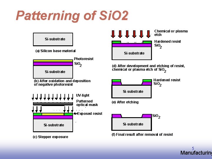
Patterning of Si. O 2 Chemical or plasma etch Si-substrate Hardened resist Si. O 2 (a) Silicon base material Si-substrate Photoresist Si. O 2 Si-substrate (d) After development and etching of resist, chemical or plasma etch of Si. O 2 Hardened resist Si. O 2 (b) After oxidation and deposition of negative photoresist UV-light Patterned optical mask Si-substrate (e) After etching Exposed resist Si-substrate (c) Stepper exposure Si. O 2 Si-substrate (f) Final result after removal of resist 5 EE 141 Manufacturing

Photo-Lithographic Process optical mask oxidation photoresist removal (ashing) photoresist coating stepper exposure Typical operations in a single photolithographic cycle (from [Fullman]). photoresist development acid etch process step spin, rinse, dry 6 EE 141 Manufacturing

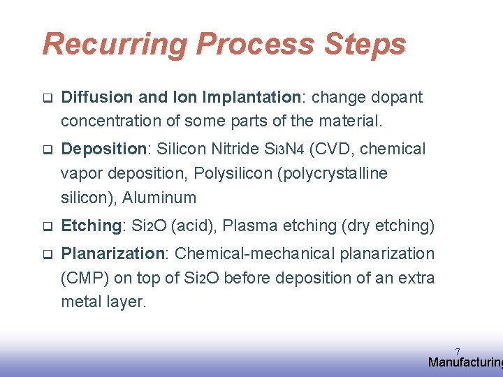
Recurring Process Steps q Diffusion and Ion Implantation: change dopant concentration of some parts of the material. q Deposition: Silicon Nitride Si 3 N 4 (CVD, chemical vapor deposition, Polysilicon (polycrystalline silicon), Aluminum q Etching: Si 2 O (acid), Plasma etching (dry etching) q Planarization: Chemical-mechanical planarization (CMP) on top of Si 2 O before deposition of an extra metal layer. 7 EE 141 Manufacturing

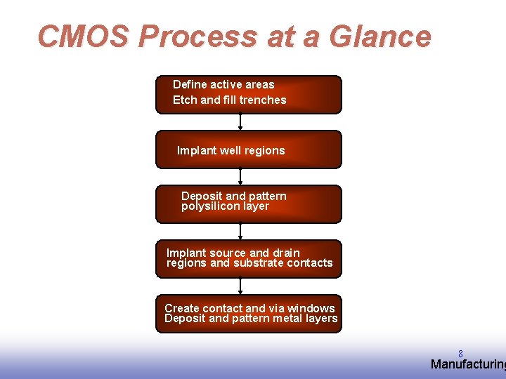
CMOS Process at a Glance Define active areas Etch and fill trenches Implant well regions Deposit and pattern polysilicon layer Implant source and drain regions and substrate contacts Create contact and via windows Deposit and pattern metal layers 8 EE 141 Manufacturing

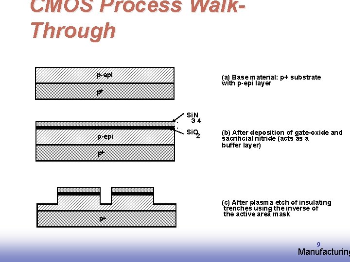
CMOS Process Walk. Through p-epi (a) Base material: p+ substrate with p-epi layer p+ Si. N 34 p-epi p+ p+ Si. O 2 (b) After deposition of gate-oxide and sacrificial nitride (acts as a buffer layer) (c) After plasma etch of insulating trenches using the inverse of the active area mask 9 EE 141 Manufacturing

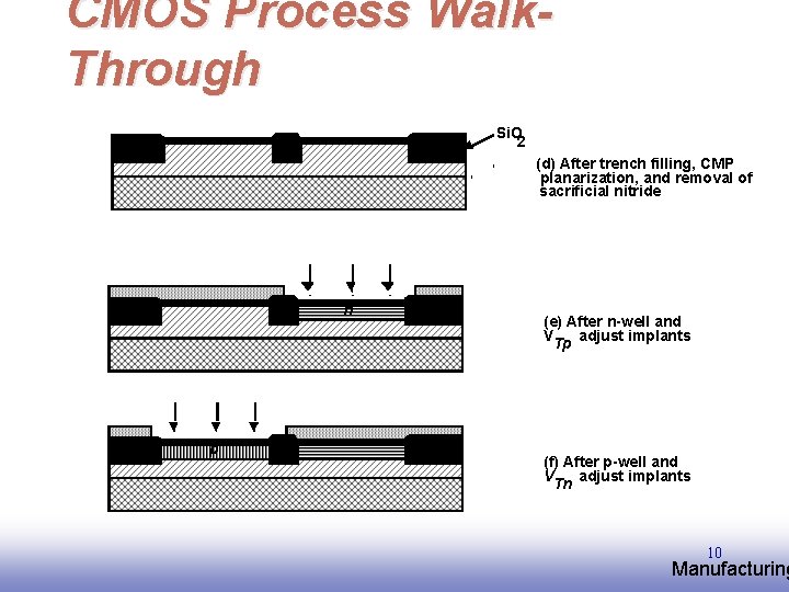
CMOS Process Walk. Through Si. O 2 (d) After trench filling, CMP planarization, and removal of sacrificial nitride n p (e) After n-well and V adjust implants Tp (f) After p-well and V adjust implants Tn 10 EE 141 Manufacturing

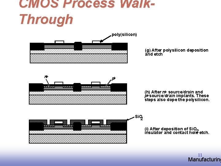
CMOS Process Walk. Through poly(silicon) (g) After polysilicon deposition and etch n+ p+ (h) After n+ source/drain and p+ source/drain implants. These steps also dope the polysilicon. Si. O 2 (i) After deposition of Si. O insulator and contact hole 2 etch. 11 EE 141 Manufacturing

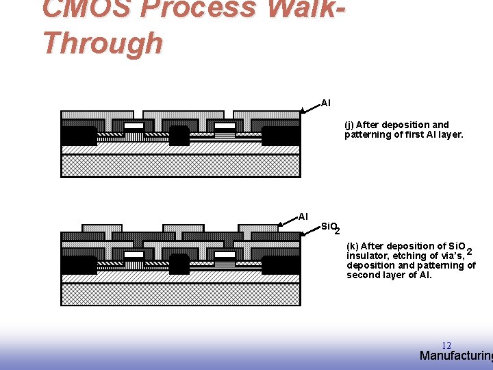
CMOS Process Walk. Through Al (j) After deposition and patterning of first Al layer. Al Si. O 2 (k) After deposition of Si. O insulator, etching of via’s, 2 deposition and patterning of second layer of Al. 12 EE 141 Manufacturing

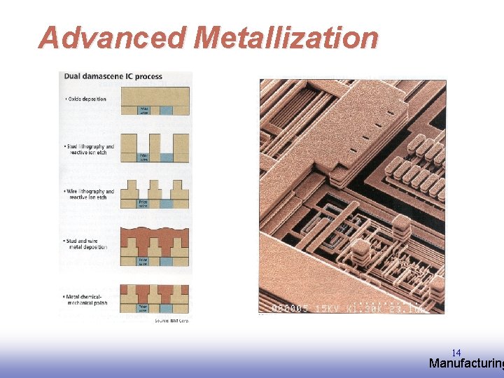
Advanced Metallization 13 EE 141 Manufacturing

Advanced Metallization 14 EE 141 Manufacturing

Design Rules 15 EE 141 Manufacturing

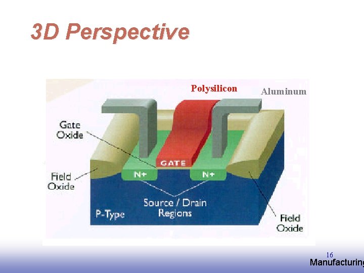
3 D Perspective Polysilicon Aluminum 16 EE 141 Manufacturing

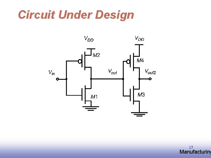
Circuit Under Design 17 EE 141 Manufacturing

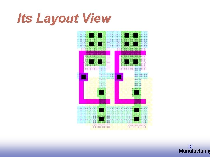
Its Layout View 18 EE 141 Manufacturing

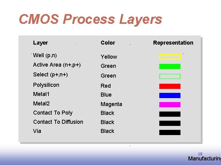
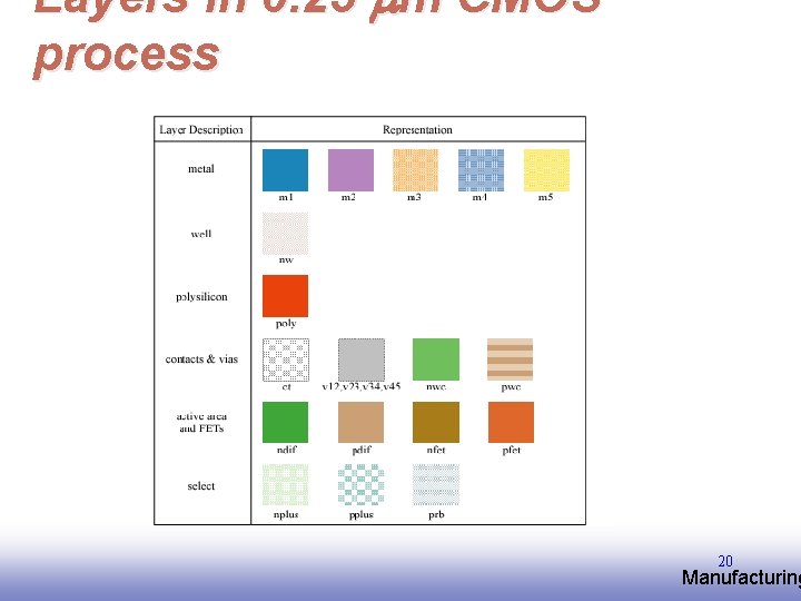
CMOS Process Layer Color Well (p, n) Yellow Active Area (n+, p+) Green Select (p+, n+) Green Polysilicon Red Metal 1 Blue Metal 2 Magenta Contact To Poly Black Contact To Diffusion Black Via Black Representation 19 EE 141 Manufacturing

Layers in 0. 25 mm CMOS process 20 EE 141 Manufacturing

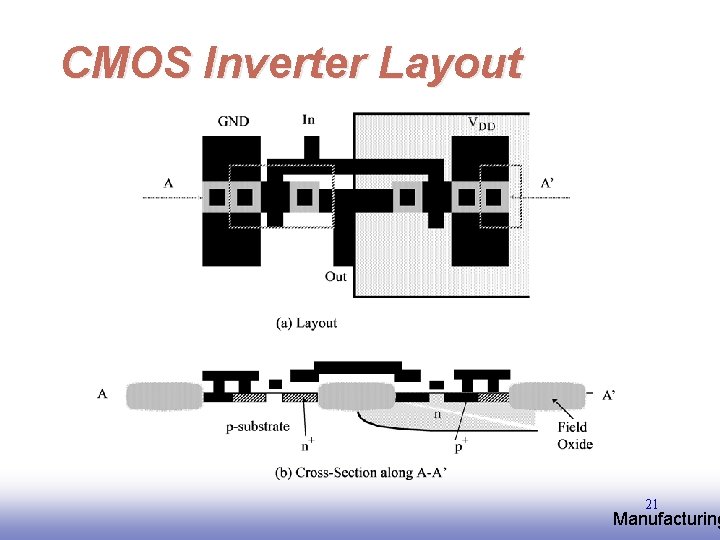
CMOS Inverter Layout 21 EE 141 Manufacturing

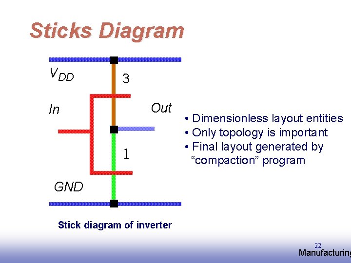
Sticks Diagram V DD 3 Out In 1 • Dimensionless layout entities • Only topology is important • Final layout generated by “compaction” program GND Stick diagram of inverter 22 EE 141 Manufacturing

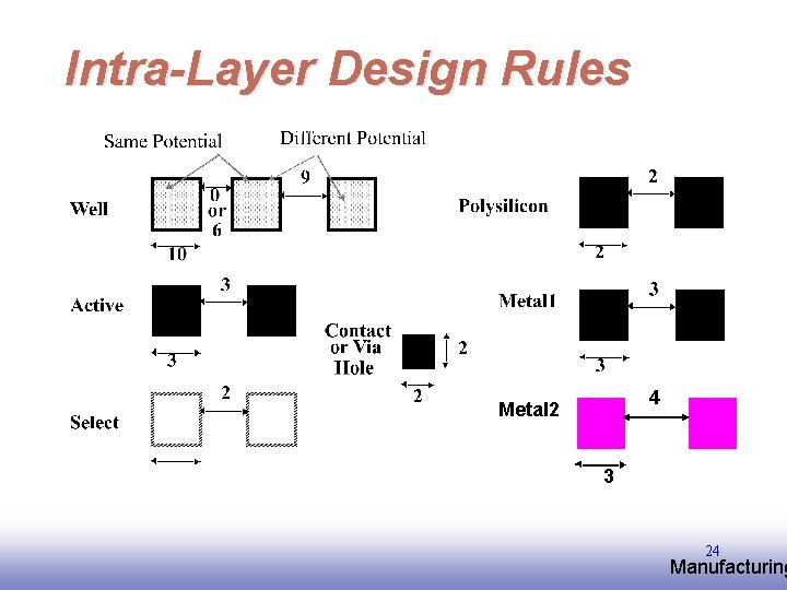
Design Rules Interface between designer and process engineer q Guidelines for constructing process masks q Unit dimension: Minimum line width § scalable design rules: lambda parameter § absolute dimensions (micron rules) q 23 EE 141 Manufacturing

Intra-Layer Design Rules 4 Metal 2 3 24 EE 141 Manufacturing

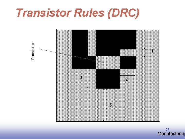
Transistor Rules (DRC) 25 EE 141 Manufacturing

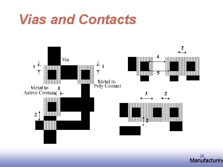
Vias and Contacts 26 EE 141 Manufacturing

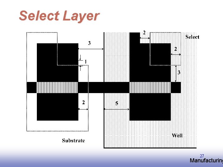
Select Layer 27 EE 141 Manufacturing

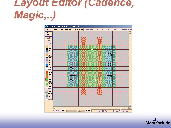
Layout Editor (Cadence, Magic, . . ) 28 EE 141 Manufacturing

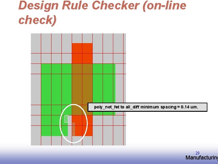
Design Rule Checker (on-line check) poly_not_fet to all_diff minimum spacing = 0. 14 um. 29 EE 141 Manufacturing

of Complexe Gate: From Chapter 6 Slides and Insert D Designing Combinational Logic Circuits March 28, 2003 30 EE 141 Manufacturing

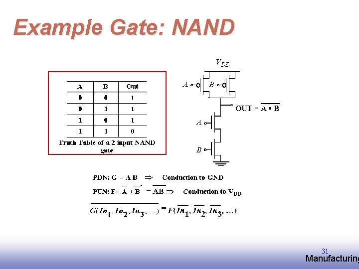
Example Gate: NAND 31 EE 141 Manufacturing

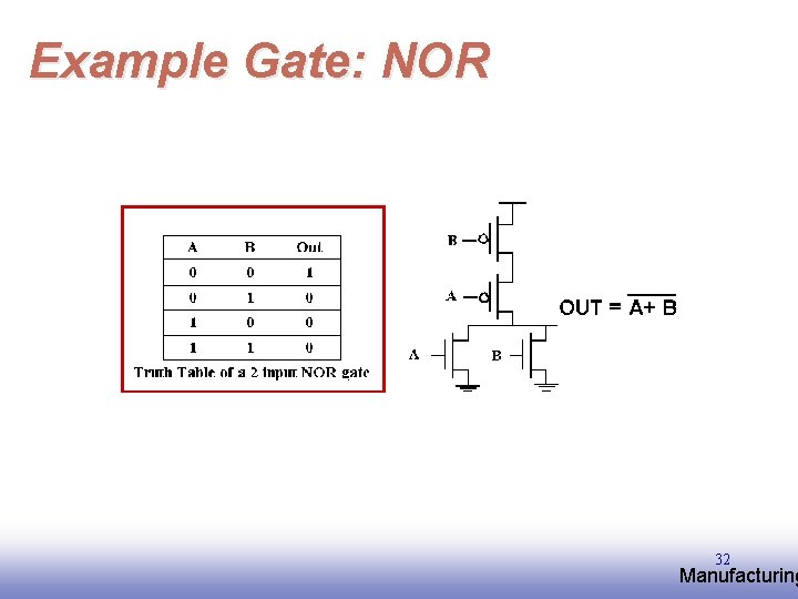
Example Gate: NOR 32 EE 141 Manufacturing

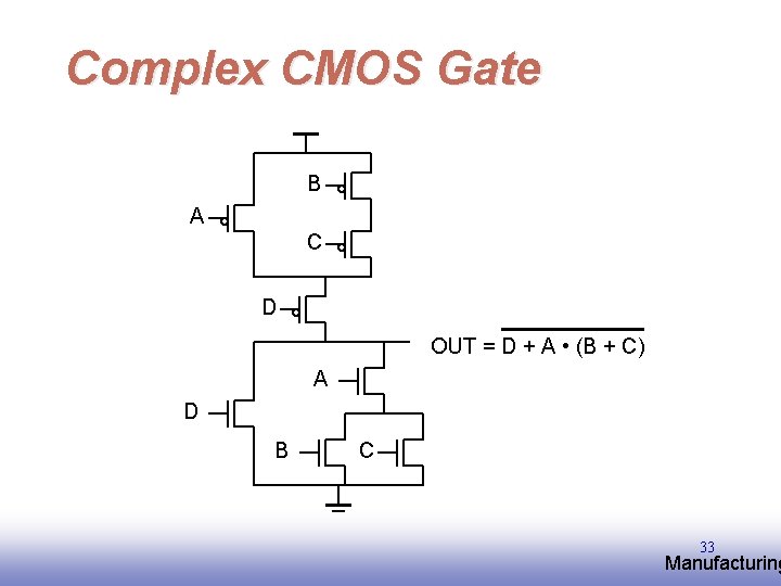
Complex CMOS Gate B A C D OUT = D + A • (B + C) A D B C 33 EE 141 Manufacturing

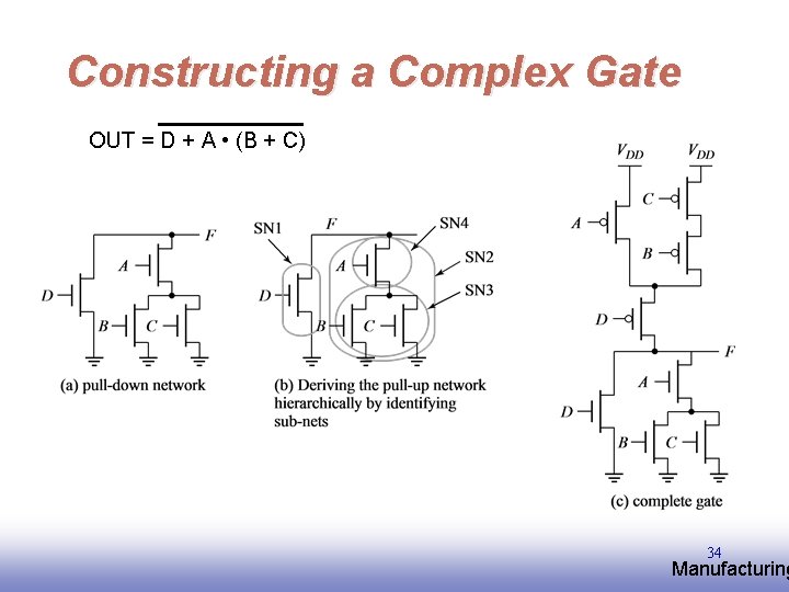
Constructing a Complex Gate OUT = D + A • (B + C) 34 EE 141 Manufacturing

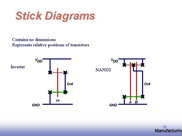
Stick Diagrams Contains no dimensions Represents relative positions of transistors VDD Inverter NAND 2 Out In GND A B 35 EE 141 Manufacturing

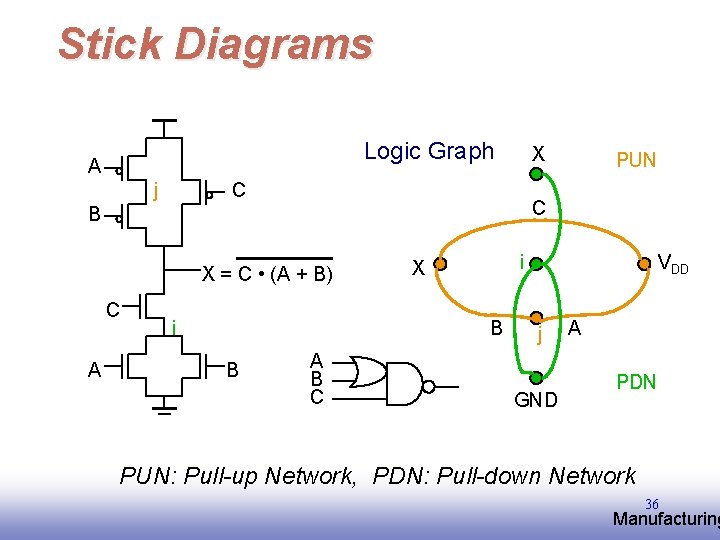
Stick Diagrams Logic Graph A j X C C B X = C • (A + B) C A i i X B B PUN A B C VDD j GND A PDN PUN: Pull-up Network, PDN: Pull-down Network 36 EE 141 Manufacturing

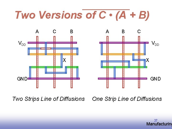
Two Versions of C • (A + B) A C B A B C VDD X GND Two Strips Line of Diffusions X GND One Strip Line of Diffusions 37 EE 141 Manufacturing

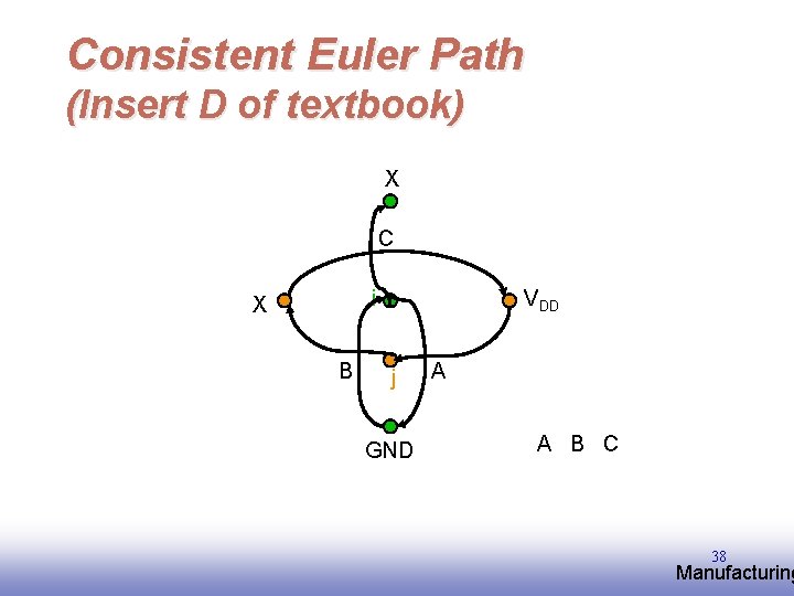
Consistent Euler Path (Insert D of textbook) X C i X B VDD j GND A A B C 38 EE 141 Manufacturing

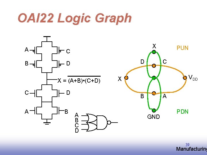
OAI 22 Logic Graph A C B D X = (A+B) • (C+D) C D A B C VDD X B A B C D PUN A GND PDN 39 EE 141 Manufacturing

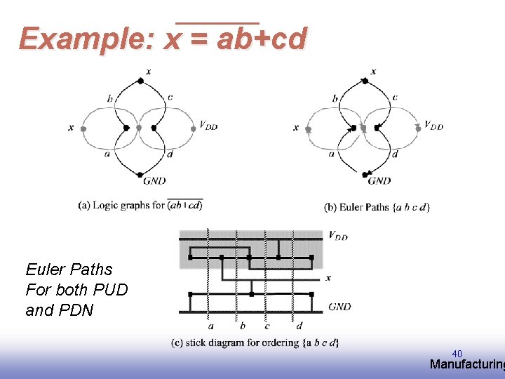
Example: x = ab+cd Euler Paths For both PUD and PDN 40 EE 141 Manufacturing

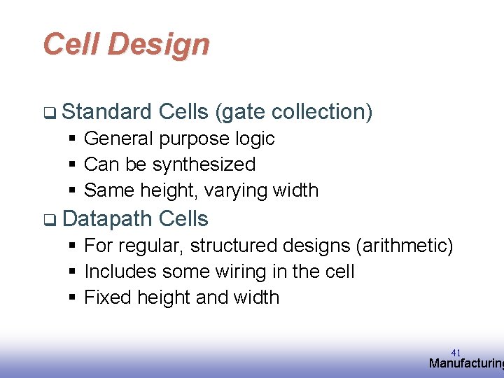
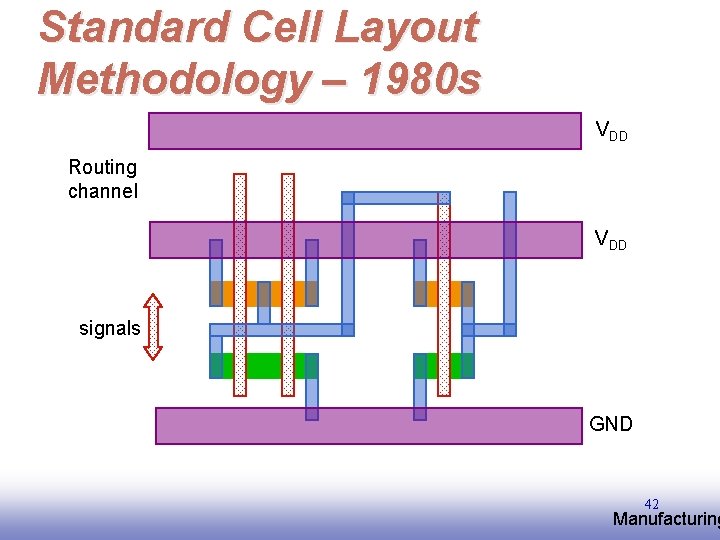
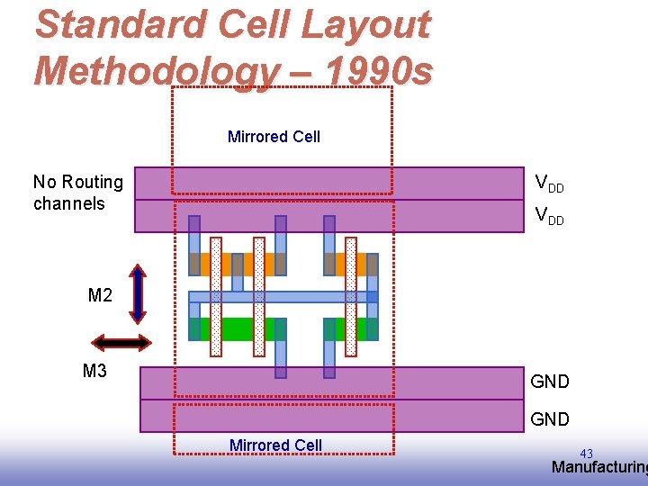
Cell Design q Standard Cells (gate collection) § General purpose logic § Can be synthesized § Same height, varying width q Datapath Cells § For regular, structured designs (arithmetic) § Includes some wiring in the cell § Fixed height and width 41 EE 141 Manufacturing

Standard Cell Layout Methodology – 1980 s VDD Routing channel VDD signals GND 42 EE 141 Manufacturing

Standard Cell Layout Methodology – 1990 s Mirrored Cell No Routing channels VDD M 2 M 3 GND Mirrored Cell EE 141 43 Manufacturing

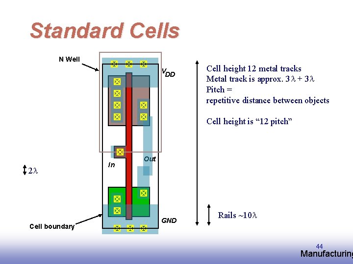
Standard Cells N Well VDD Cell height 12 metal tracks Metal track is approx. 3 + 3 Pitch = repetitive distance between objects Cell height is “ 12 pitch” 2 Cell boundary In Out GND Rails ~10 44 EE 141 Manufacturing

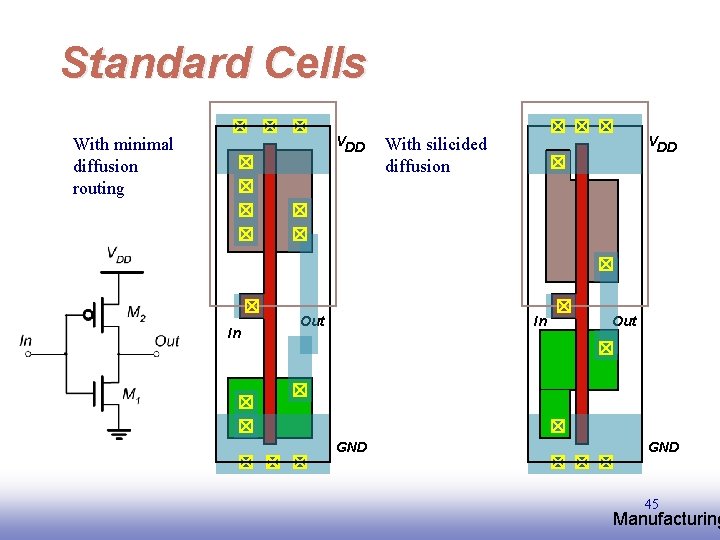
Standard Cells VDD With minimal diffusion routing In Out VDD With silicided diffusion In GND Out GND 45 EE 141 Manufacturing

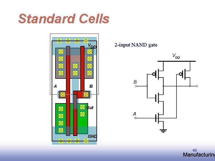
Standard Cells VDD A 2 -input NAND gate B Out GND 46 EE 141 Manufacturing

CMOS Fabrication and Layout • See the supplement data in Web! • http: //access. ee. ntu. edu. tw 47 EE 141 Manufacturing