Chapter 2 Electrical Components and Circuits Components Electrical


 Series circuits Fig 2 -1. A battery, a switch,")


 Parallel Circuits Resistors in parallel at point A Kirchhoff's current law to point")

 Calculate a) the total resistance, b) the current from the battery,")
 ( --- + --- ) = --R 2 R 3")


 ; DC, AC의 크기비교 ; 두 전류에 의한 저항에서 야기되는")

 A series RC circuit. Time response of circuit")
 Capacitance ① a momentary current ② current ceases")


 At sufficiently high frequencies & capacitance, φ become negligible & I")


 high pass filter and (b)low-Pass Filters")


 FET - The insulated gate field effect transistor. → 109~1014")
 structure, (b) symbol, (c) performance")
 Current enhancement is brought about by application of a positive potential")


- Slides: 74
Chapter 2. Electrical Components and Circuits Components
Electrical Components: Electric current; the motion of a charge through a medium. Electric units; the unit of charge (or quantity of electricity) C(coulomb) → 0. 001111800 g of silver ion → Charge for reduction to silver metal. 1 Faraday = 9. 649 x 104 coulombs 1 Faraday ; Deposition of Ag 107. 868 g of 1 gram equivalent ↳ (6. 02 x 1023 charged particle), I = d. Q/dt (Q : charge, A : ampere)
2 A Direct-Current Circuits and Measurements - Direct current; Q -> proportional to time. - Alternating current; Q -> periodically change. 2 A-1 Laws of Electricity Electrical potential (V) ; 공간의 한 점에서 다른 점까지 1개의 전하를 움직이는데 는 일. V ; volt → joule/conlomb (W/Q = V) = (I․R) R ; ohm → R의 단위 Ω(R = ρℓ/A) ↳ Ohm's law G ; 저항의 역수(electrical conductance) Ω-1, S I ; Ampere P ; Electrical power. joules/sec, W P = dw/dt = V․d. Q/dt = V․I P = (I․R)․I = I 2 R. joule's law
Kirchhoff's Laws - Current low ; the algebraic sum of currents around any point in a circuit is zero. -Voltage low ; the algebraic sum of the voltages around a closed electrical loop is zero. Power Law P = IV P = I 2 R = V 2/R
2 A-2 Direct-Current Circuits 1) Series circuits Fig 2 -1. A battery, a switch, & three resistors in series.
ⓐ 점 D에서 kirchhoff's law 적용 I 4 - I 3 = 0 or I 4 = I 3 , I 3 = I 2 at point C. * the current is the same at all points I = I 1 = I 2 = I 3 = I 4 ⓑ Voltage low V - V 3 - V 2 - V 1 = 0 or V = V 1 + V 2 + V 3 by ohm's law V = 1(R 1 + R 2 + R 3) = IReq ∵ Req = R 1 + R 2 + R 3 IR 1 = V 1 , V 2 = IR 2 , V 3 = IR 3 V 1 = I 1 R 1 = IR 1 (2 -9)
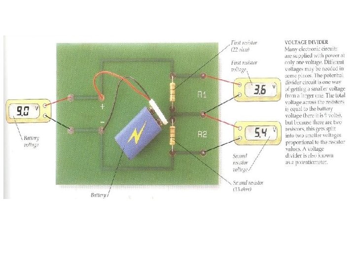
Voltage dividers ; Fig 2 -3 a → series connection of resistor ↳ discrete increment
- Potentiometer; continuously variable
2) Parallel Circuits Resistors in parallel at point A Kirchhoff's current law to point A I 1 + I 2 + I 3 - It = 0 It = I 1 + I 2 + I 3
- Applying Kirchhoff's voltage law I 1 = V/R 1 V - I 1/R 1 =0 V= I 1 R 1 I 2 = V/R 2 V - I 2/R 2 =0 V = I 2 R 2 I 3 = V/R 3 V = I 3 R 3 It = I 1 + I 2 + I 3에 위식 代入 V V It = --- + --Rp so that R 1 R 2 R 3 1 1 --- = --- + --Rp G=1/R V 1 = V 2 = V 3 = V R 1 R 2 R 3 G p = G 1 + G 2 + G 3 - Parallel resistances create a current divider. I 1 V/R 1 1/R 1 G 1 --- = ----- = --It V/Rp 1/Rp Gp Rp G 1 or I 1 = It --- = It --R 1 Gp
(Ex. 2 -1) Calculate a) the total resistance, b) the current from the battery, c) the current present in each of the resistors, and d) the potential drop across each of the resistors.
1 1 1 a) ( --- + --- ) = --R 2 R 3 R 2, 3 1 1 1 3 --- = --- + --- = --R 20 40 40 b) The current ; V = I·R R 2, 3 = 13. 3Ω V 15 I = ----- = 0. 67 A Rs 22. 3 c) V = V 1 + V 2 + V 3 V 1 = I 1 R 1 = 6. 03 I = I 2 = I 3 이므로 9. 0 V 1 = 15 x ------ = 6. 0 V (9. 0 + 13. 3) 13. 3 V 2 = V 3 = V 2, 3 = 15 x ------ = 9. 0 V 22. 3 d) R 1에서 I 1 = I = 0. 67 A I 2 = 9. 0/20 = 0. 45 A I 3 = 9. 0/40 = 0. 22 A
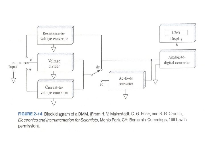
2 A-3 Direct Current, Voltage, and Resistance Measurements Digital Volmeters and Multimeters D’Arsonval moving-coil meter Digital Voltmeters and Multimeters. Power Source, display, A/D converter
The Loading Error in Potential Measurements The Loading Error in Current Measurements
See equations 2 -19 and 2 -20
2 B Alternating current Circuits Alternating voltage and current: 화가 계속 반복되는 전압 또는 전류. 시간에 따라 방향과 크기가 변화하며 똑같은 변 ( the simplest alternating waveform is sine- wave volt or current. ) - Period (Tp); The time required for the completion of one cycle - Cycle; one complete revolution - Frequency(f) [HZ]; time number of cycles per second f = 1/tp (2 -21)
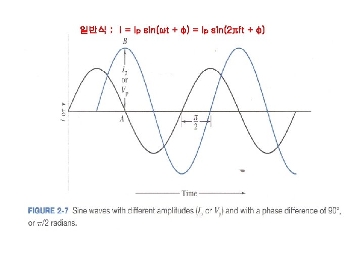
2 B-1 Sinusoidal Signals The AC: produced by rotation of a coil in a magnetic field. A pure sine wave → 일정한 각속도로 회전 하는(시계방향) IP의 vector로 표시. (여기서 Ip : amplitude. ) 주기 t 내에 2π radian 의 속도로 회전 할 때 ω = 2π/tp = 2πf Any time t에서 instantaneous value → Vpsin ωt Vp; maximum or peak voltage; the amplitude 순간 전류 : ⅰ= Ip sin ωt = Ip sin 2πft 순간 전압 : v = Vp sin ωt = Vp sin 2πft Out of phase by 90 o Phase difference : phase angle(φ) 일반식 ; ⅰ= Ip sin(ωt + φ) = Ip sin(2πft + φ)
Sinusoidal signals ;
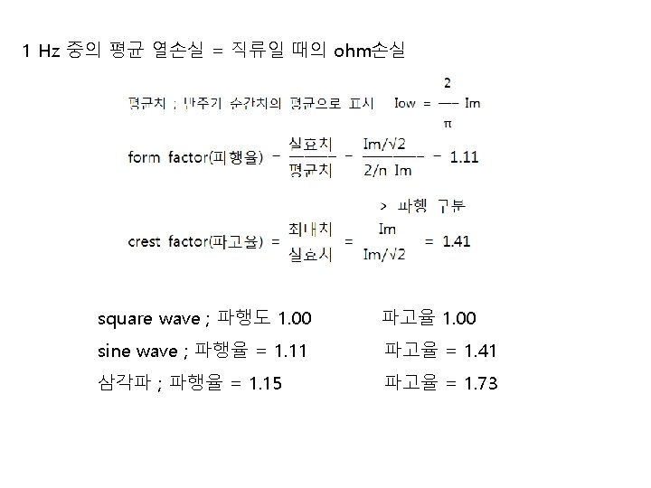
(rms current & voltage) ; DC, AC의 크기비교 ; 두 전류에 의한 저항에서 야기되는 Joule heat DC = the effective value of a sinusoidal, current Report, heating effect of AC is calculated by averaging I 2 R losses even complete cycle
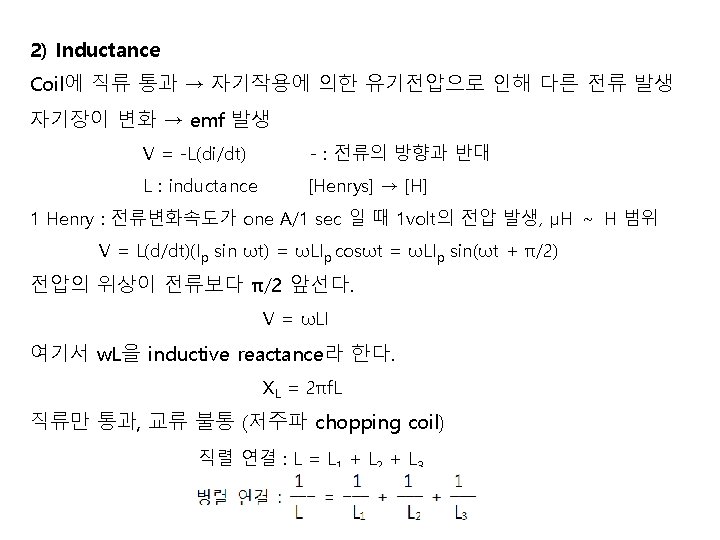
2 B-2 Reactance in Electrical Circuits Reactance - capacitance : capacitor inductance : inductor Use ; ① converting alternating current to DC or the converse ② discriminating among signals of different frequencies or separating ac & dc signals. Capacitors 구성; a pair of conductors separated by a thin layer of a dielectric substance
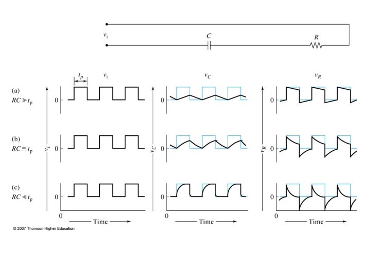
Position 1 Figure 2 -8. (a) A series RC circuit. Time response of circuit when switch S is (b) in position 1 and (c) in position 2. Position 2
2 B-3 Capacitors and Capacitance 1) Capacitance ① a momentary current ② current ceases → to be changed ③ switch을 2로 discharge. Capacitor ① 과 ② 사이에서 switch off; 전하가 저장 The quantity of electricity Q → 판 넓이, 모양, 공간, 절연체 의 유전상수에 의해 결정 (one-farad capacitor stores 1 Q of charge per applied volt. )
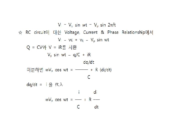
Rate of current and voltage changes in an RC circuit By Kirchhoff 의 voltage law Vi = v c + v R Vi = q/C + i. R Vi = constant : Instantaneous voltage across the resistor
: Ohm’s law to eq. 2 -35 Phase relations between current and voltage in an RC circuit Fig. 2 -8 c
Rate of Current & Potential Change across RL circuit. RC circuit와 동일한 방법으로 처리 v. R = Vi( I - e-t. R/L ) v. L = Vi e-t. R/L L/R : time constant
2 B-4 Response of Series RC Circuits to Sinusoidal Inputs signal
Ip
(1/ωC = Xc) At sufficiently high frequencies & capacitance, φ become negligible & I & v are in phase. 1/ωC은 저항 R에 비해 무시 可. ↳ 전류가 잘 흐름 At very low frequencies, the phase angle; π/2
Voltage, current and phase Relationships for series RL circuit
Figure 2 -9 90 o phase difference between v and i
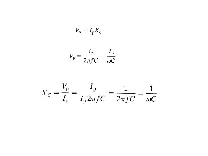
Capacitive & Inductive Reactance ; impedance Xc = 1/w. C = 1/2πf. C XL = w. L = 2πf. L Impedance Z ; 교류회로에서 전압과 전류의 크기의 비(직류회로의 저항에 해당) At, RC circuit Z = √R 2 + Xc 2 Z = √R 2 + XL 2 Ip = Vp/Z 저항과 차이점 : ① frequency dependent ② current와 voltage 사이에 phase difference
1 Faraday ; 1 V의 전위치에 의해 양극판에 축적된 전하의 크기가 1 C일 때의 capacitance. ( μF, PF) V = 1/C ∫idt = 1/C∫ Ip sin wt dt = -1/wc Ip cos wt = 1/wc Ip sin(wt - π/2) ∵ Vp = 1/wc Ip, V = (1/wc) I 1/wc = Xc → capacitive reactance 단위 Ω Xc = -1/wc, V =│Xc│I
Figure 2 -10
<Vector diagrams for Reactive Circuits> V가 ⅰ보다 90°늦다. at capacitance V가 ⅰ보다 90°빠르다. at inductance Z = √R 2 + (XL - Xc)2 Z = √R 2 + Xc 2 , φ = -arctan Xc/R Z = √R 2 + XL 2 , φ = -arctan XL/R Z = √R 2 + (XL + Xc)2 φ = -arctan (XL + Xc) / R (XL > Xc 인 경우) ex) ① peak current ② voltage drop Z = √(50)2 + (40 - 20)2 = 53. 8Ω Ip = 10 v/53. 8 = 0. 186 A Vc = 0. 186 x 20 = 3. 7 V VR = 0. 186 x 50 = 9. 3 V VL = 0. 186 x 40 = 7. 4 V
2 B-5 Filters Based on RC Circuits High-pass & Low-Pass Filters RC & RL circuits → low f component를 지나는 동안 high-f signals을 낮추기 위해 filter로 사용 (low pass filter) or 역이 성립. ① RC circuit에서 high-pass filter Vo : across the resistor R
(a) high pass filter and (b)low-Pass Filters
Low pass filter
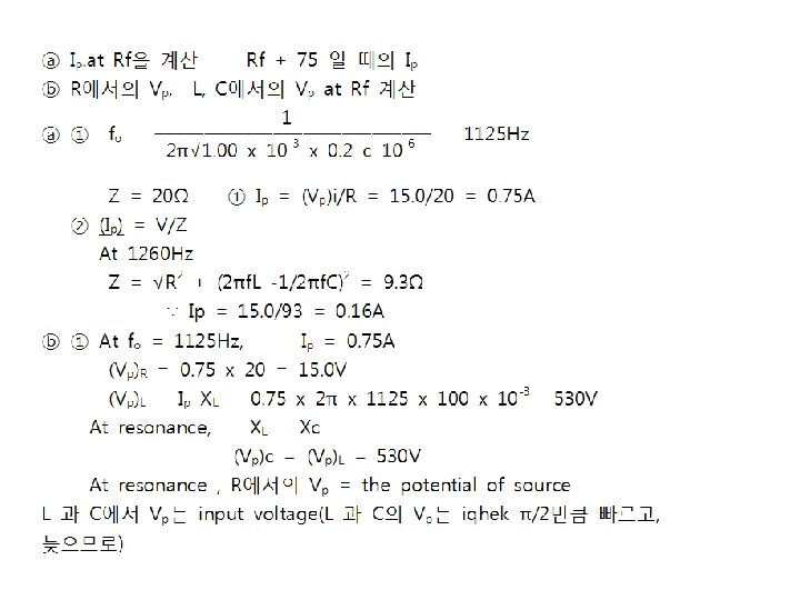
2 B-6 The Response of RC Circuits to Pulsed Inputs <Resonant Circuits> impedance Z가 최소 즉 XL = Xc 일 때 전류 I = E/Z = E/R ↳ the condition of Resonance resonant frequency fo ; 1/2πfo. C = 2πfo. L ∵ fo = 1/2π√LC ex) (Vp)i = 15. 0 V (peak voltage), L = 100 m. H, R = 20Ω, C = 1. 200μF.
2 B-7 Alternating Current, Voltage, and Impedance Measurements Parallel Resonance Filters Xc = XL fo = 1/2π√LC Z of the parallel circuit Z = √R 2 + (XLXc/Xc-XL)2 At parallel circuit at resonance → Z는 최대 → maximum voltage drop 生 → tank circuit Behavior of RC Circuits with pulsed inputs RC 회로에 pulse 加 → various form (with of pulse time const) 사이의 관계에 의존 Simple Electrical Measurements Galvanometers → DC의 전류, 저항 측정 원리 : the current in duceol motion of a coil suspended in a fixed magnetic field. ⇒ D'arsonval movement or coil. He Ayrton Shunt : to vary the range of a galvanometers p 29. 예제 참조 ☆ measurement of current and voltage.
2 C Semiconductors and Semiconductor Devices Semiconductors -Electronic circuits contain one or more nonlinear devices, such as transistors, semiconductor diodes, and vacuum or gas-filled tubes. -Nonlinear components ; rectification (from ac to dc ), amplitude modulation, or frequency modulation. -Vacuum tube (in the 1950 s)→ Semiconductor based diodes and transistors → integrated circuits (Tr, R, C & conductor) -Semiconductor 장점 : low cost, low power consumption, small heat generation, long life and compactness.
2 C-1 Properties of silicon & germanium semiconductors. -Sufficient thermal agitation occurs at room temp. to liberate an occasional electron from its bonded state, leaving it free to more through the crystal lattice and thus to conduct electricity. -Hole : positively charged region. -Electron: negatively charged region. -Hole & electron 의 이동방향 반대. -Doping of arsenic or antimony (Group Ⅴ) → n type of indium or gallium (Group Ⅲ) → p type Positive holes are less mobile them free electrons. Conductivity of n type >conductivity of p type.
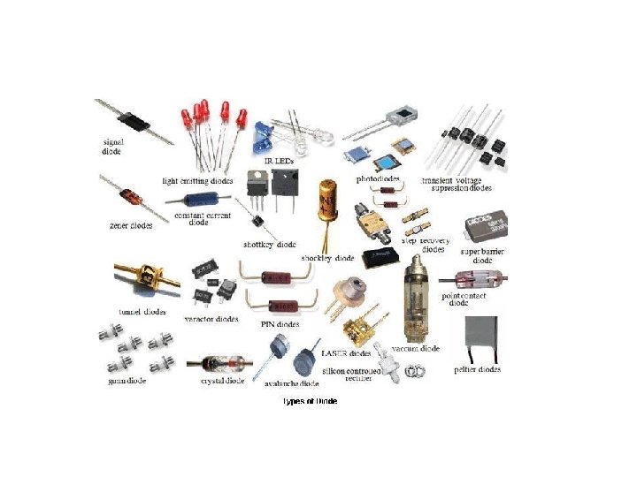
2 C-2. Semiconductor Diodes Pn junction motion → diode is a nonlinear device that has greater conductance in one direction than in another. Figure 2 -15 A pn junction diode (c) forward - bias (d) reverse - bias → depletion layer 생성 : conductance 10 -6~10 -8
Figure 2 -16 I - V cures for semiconductor Diodes The voltage at which the sharp increase in current occurs under reverse bias is called the Zener breakdown voltage.
2 C-3 Transistors : Amplifying device -Bipolar -Field effect transistor. Bipolar Junction Transistors : pnp, npn tr. Bipolar junction transistors(BJTs) may be viewed as two back-to-back semiconductor diodes.
Electrical Characteristics of a BJT The discussion that follows focuses on the behavior of a pnp-type BJT. Mechanism of Amplification with a BJT Turning again to Fig 2 -18, holes are formed at the ptype emitter junction through removal of electrons by the two dc sources, namely, the input signal and the power supply.
Fig 2 -17. Two types of BJTs. The mechanism of amplification with a bipolar transistor. pnp on ∽ n layer ~ 0. 02 mm thickness, p>>n layer. (수백배 이상), ∴The concentration of holes in p >> that of electrons in n layer
Fig 2 -18. Current in a commonemitter circuit with a transistor.
① P-type emitter junction 에서 hole 생성 ② ①번의 hole 이 very thin n-type base 로 이동 - electron 과 결합 (base current IB유발) ③ 대부분의 hole 은 base를 통해 drift 되어 collector junction 으로 attracting ④ 여기서 power supply로부터 나온 electron 과 combined 되어 전류 흐 름 (Ic) The no of current carrying holes is a fixed multiple of the number of electrons supplied by the input base current.
Field Effect Transistors (FET) FET - The insulated gate field effect transistor. → 109~1014 Ω 의 input impedance → MOSFET (metal oxide semiconductor FET) n- channel MOSFET The gate is a cylindrical p-type semiconductor surrounding a center core of n -doped material called the channel. Two isolated n regions are formed in a p-type substrate. 위의 n. p regions 을 silicon dioxide로 insulating
Fig 2 -19. An n-channel enhancement mode MOSFET: (a) structure, (b) symbol, (c) performance characteristics.
(n-channel junction FET) Current enhancement is brought about by application of a positive potential to the gate: Gate 에 “+" induce “-“ substrate channel below the layer of Si. O 2 Depletion mode →to conduct in the absence of a gate voltage and to become nonconducting as potential is applied to the gate. The reverse bias is applied to the gate -> the supply of electrons in the channel is depleted. → channel 저항 증가→전류감소.
2 D Power Supplies and Regulators most ps contains a voltage regulator. Fig 2 -20. Diagram showing the components of a power supply and their effects on the 115 -V line voltage.
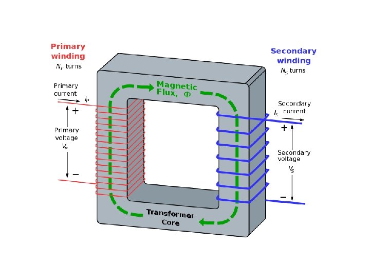
2 D-1 Transformers The voltage from the ac power lines is readily increased or decreased by means of a powe transformer such as that shown schematically in Fig 2 -21. VX = 115 X N 2/N 1 N 2 and N 1 are the no of turns in the secondary and primary coils. 2 D-2 Rectifiers Fig 2 -22 shows three type of rectifiers and their output-signal forms. ①Half wave rectifier ②Full wave rectifier ③bridge rectifier ①: ②; 그림 ③ 그림
Fig 2 -21. Schematic of a typical power transformer with multiple secondary windings.
D 2, D 3 → conduct on the alternate D 4 and D 1 conduct Since two diodes are in series with the load, the output voltage is reduced by twice the diode drop. Fig 2 -22. Three types of rectifiers: half-wave, full-wave, and bridge.
Fig 2 -23. Filtering the output from a rectifier. In order to minimize the current fluctuations. L section filter : S 은 직렬 C는 병렬 연결. ⇒ peak to peak ripple can be reduced.
2 D-3 Voltage Regulators Fig 2 -24. Zener-stabilized voltage regulator. Fig 2 -24 illustrates a simple voltage regulator that use a Zener diode : breakdown condition 하에서 작동. Under breakdown condition, a current change of 20 to 30 m. A may result from a potential change of 0. 1 V or less.
2 E Readout Devices Fig 2 -25. Basic analog oscilloscope component
2 E-1 Oscilloscopes Cathode-Ray Tubes Fig 2 -26 is a schematic that shows the main components of a CRT. Horizontal and vertical Control Plates Input signals are applied to two sets of two set of plates, one of which deflects the beam horizontally and the other vertically. Trigger Control To steadily display a repetitive signal, such as a sine wave, on the screen, it is essential that each sweep begin at an identical place on the signal profile.
Figure 2 -26. Schematic of a CRT
2 E-2 Recorders The typical laboratory recorder is an example of a servosystem, a null device that compares two signals and then makes a mechanical adjustment that reduces their difference to zero. Fig 2 -27. Schematic of self-balancing recording potentiometer
2 E-3 Alphanumeric Displays The output from digital equipment is most conveniently displayed in terms of decimal numbers and letters, that is, in alphanumeric form. 2 E-4 Computers Many modern instruments use computers and computer monitors as readout devices.