Chapter 2 Chip Basics Time Area Power Reliability
Chapter 2 Chip Basics: Time, Area, Power, Reliability, Configurability Computer System Design System-on-Chip by M. Flynn & W. Luk Pub. Wiley 2011 (copyright 2011) soc 2. 1
Basic design issue: Time • clocking • pipelining – optimal pipelining – pipeline partitioning – wave pipelining and low overhead clocking soc 2. 2
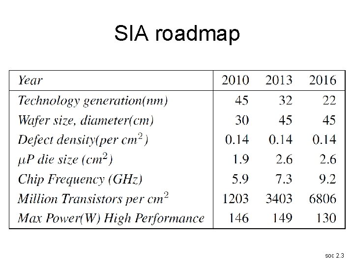
SIA roadmap soc 2. 3
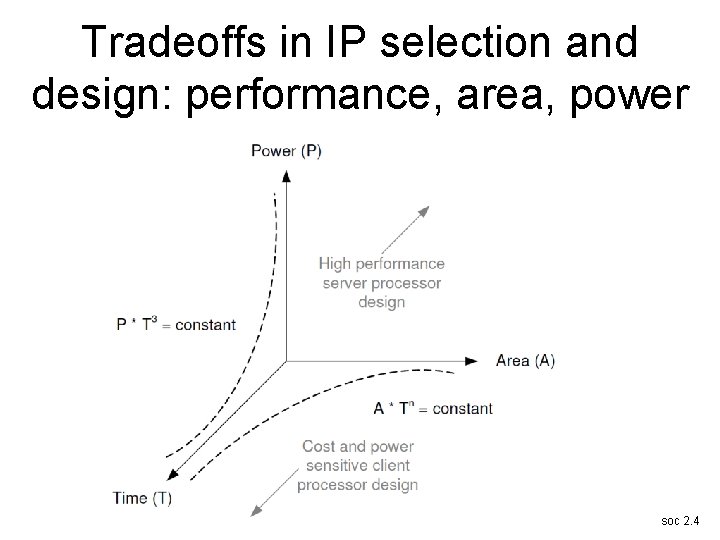
Tradeoffs in IP selection and design: performance, area, power soc 2. 4
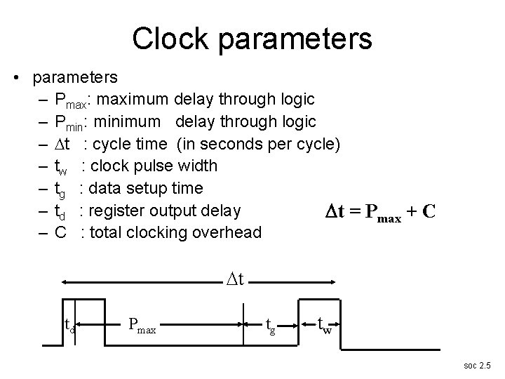
Clock parameters • parameters – Pmax: maximum delay through logic – Pmin: minimum delay through logic – t : cycle time (in seconds per cycle) – tw : clock pulse width – tg : data setup time – td : register output delay t = Pmax + C – C : total clocking overhead t td Pmax tg –tw soc 2. 5
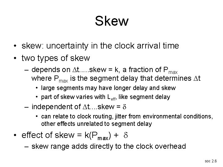
Skew • skew: uncertainty in the clock arrival time • two types of skew – depends on t. . . skew = k, a fraction of Pmax where Pmax is the segment delay that determines t • large segments may have longer delay and skew • part of skew varies with Leff, like segment delay – independent of t. . skew = • can relate to clock routing, jitter from environmental conditions, other effects unrelated to segment delay • effect of skew = k(Pmax) + – skew range adds directly to the clock overhead soc 2. 6
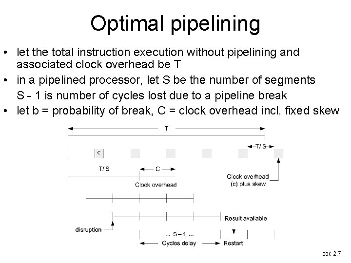
Optimal pipelining • let the total instruction execution without pipelining and associated clock overhead be T • in a pipelined processor, let S be the number of segments S - 1 is number of cycles lost due to a pipeline break • let b = probability of break, C = clock overhead incl. fixed skew soc 2. 7
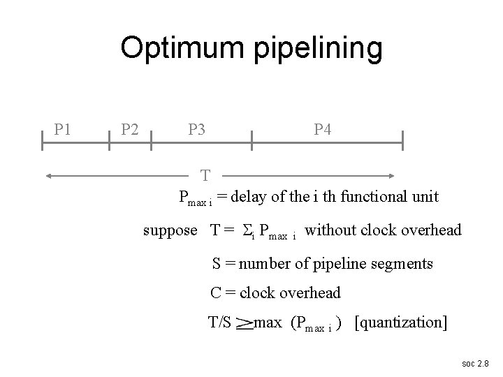
Optimum pipelining P 1 P 2 P 3 P 4 T Pmax i = delay of the i th functional unit suppose T = i Pmax i without clock overhead S = number of pipeline segments C = clock overhead T/S max (Pmax i ) [quantization] soc 2. 8
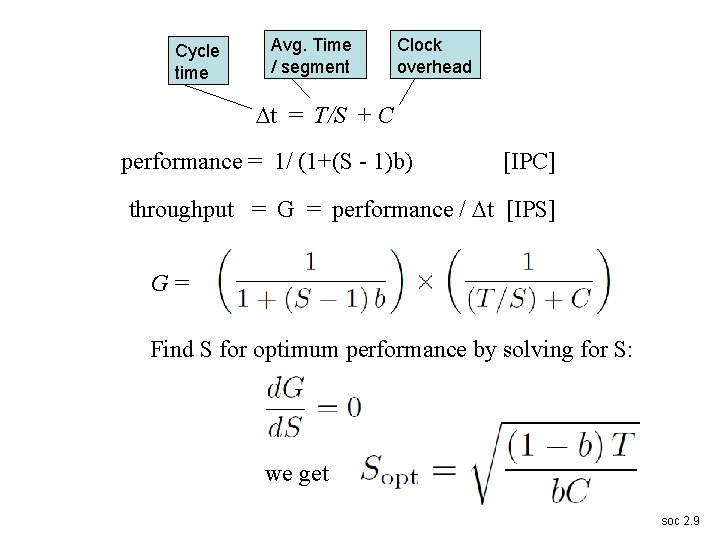
Cycle time Avg. Time / segment Clock overhead t = T/S + C performance = 1/ (1+(S - 1)b) [IPC] throughput = G = performance / t [IPS] G= Find S for optimum performance by solving for S: we get soc 2. 9
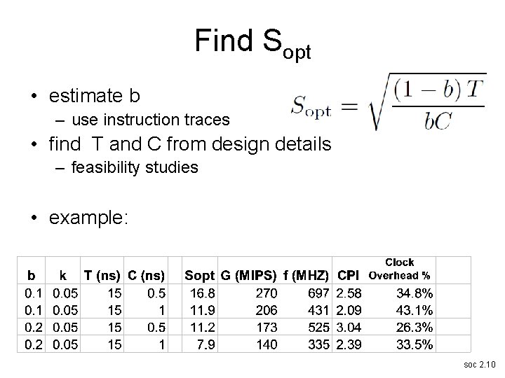
Find Sopt • estimate b – use instruction traces • find T and C from design details – feasibility studies • example: soc 2. 10
Quantization + other considerations • quantization effects – T cannot be arbitrarily divided into segments – segments defined by functional unit delays – some segments cannot be divided; others can be divided only at particular boundaries • some functional operations are atomic – cycle: usually not cross function unit boundary • Sopt – ignores cost/area of extra pipeline stages – ignores quantization loss – largest S to be used soc 2. 11
Microprocessor design practice • tradeoff around design target • optimal in-order integer RISC: 5 -10 stages – performance: relatively flat across this range – deeper for out-of-order or complex ISA (e. g. Intel Architectures) • use longer pipeline (higher frequency) if – FP/multimedia vector performance important – clock overhead low • else use shorter pipeline – especially if area/power/effort are critical soc 2. 12
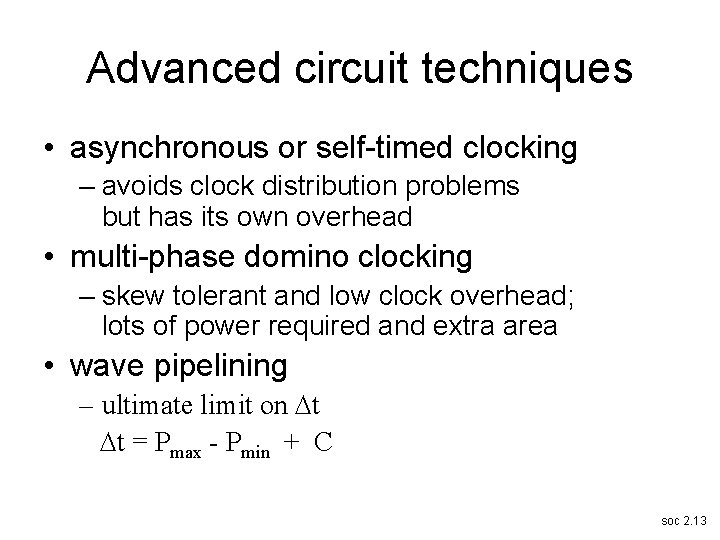
Advanced circuit techniques • asynchronous or self-timed clocking – avoids clock distribution problems but has its own overhead • multi-phase domino clocking – skew tolerant and low clock overhead; lots of power required and extra area • wave pipelining – ultimate limit on t t = Pmax - Pmin + C soc 2. 13
Basic Design Issues: Silicon Area, Power, Reliability, Reconfiguration • • • die floorplanning methodology area-cost model power analysis and model reliability reconfigurable design soft processors soc 2. 14
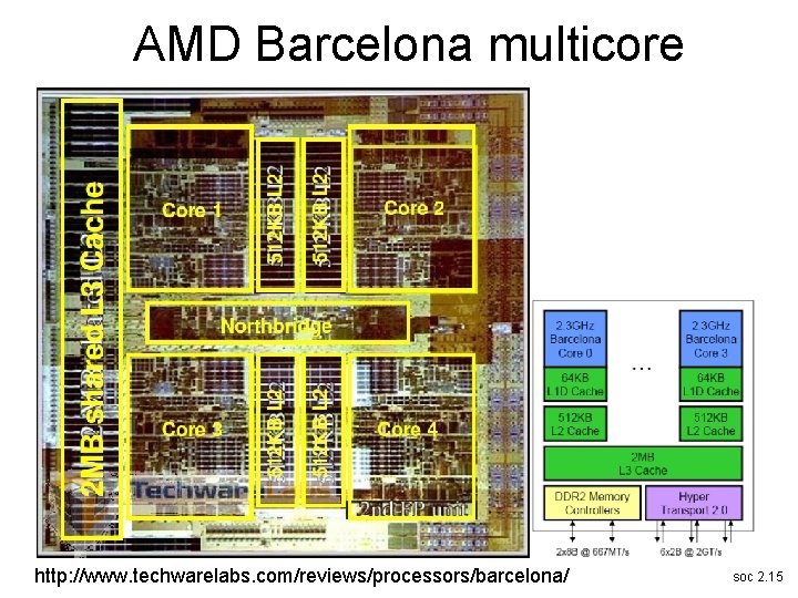
AMD Barcelona multicore http: //www. techwarelabs. com/reviews/processors/barcelona/ soc 2. 15
Die floorplanning methodology • pick target cost based on market requirements • determine total area available within cost budget – defect and yield model • compute net available area for processors, caches and memory – account for I/O, buses, test hooks, I/O pads etc. • select core processors and assess area and performance • re-allocate area to optimize performance – cache, signal processors, multimedia processors, etc. soc 2. 16
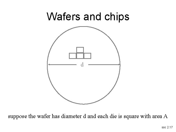
Wafers and chips d suppose the wafer has diameter d and each die is square with area A soc 2. 17
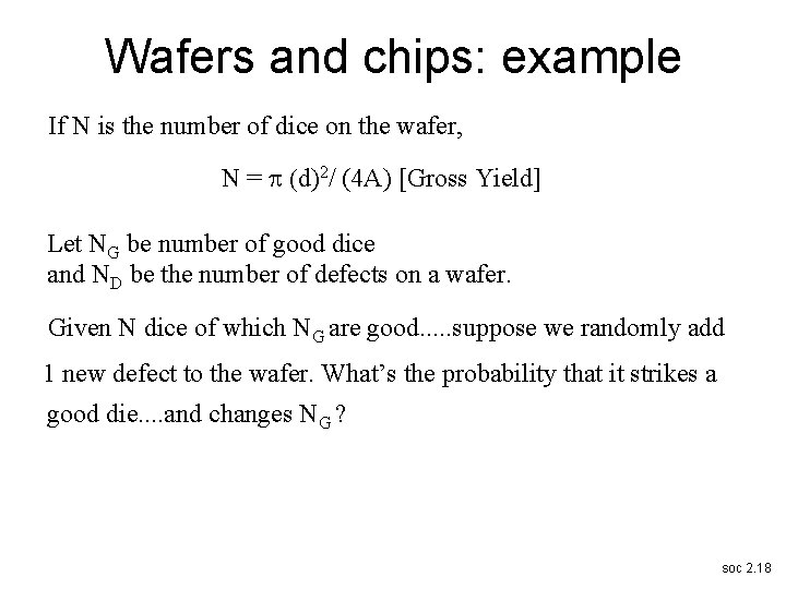
Wafers and chips: example If N is the number of dice on the wafer, N = d)2/ (4 A) [Gross Yield] Let NG be number of good dice and ND be the number of defects on a wafer. Given N dice of which NG are good. . . suppose we randomly add 1 new defect to the wafer. What’s the probability that it strikes a good die. . and changes NG ? soc 2. 18
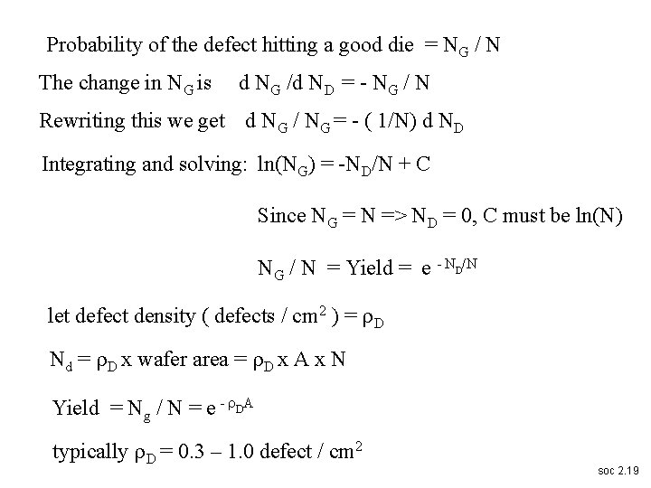
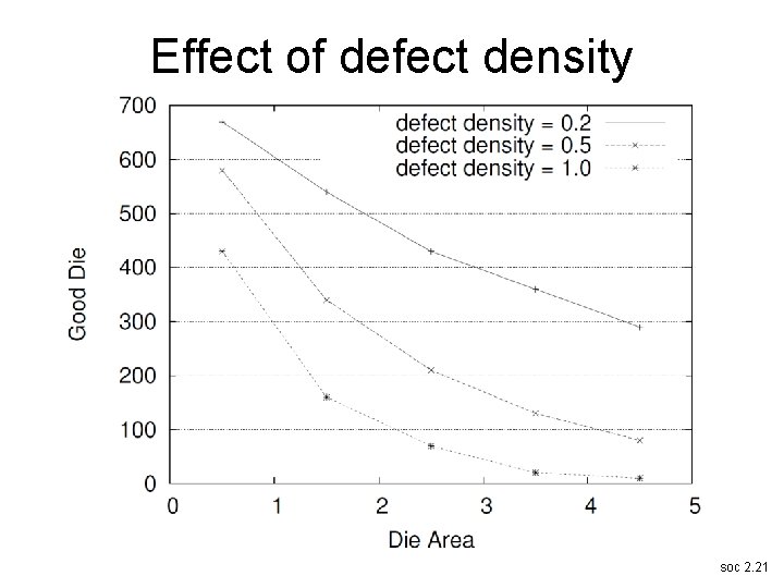
Probability of the defect hitting a good die = NG / N The change in NG is d NG /d ND = - NG / N Rewriting this we get d NG / NG = - ( 1/N) d ND Integrating and solving: ln(NG) = -ND/N + C Since NG = N => ND = 0, C must be ln(N) NG / N = Yield = e - ND/N let defect density ( defects / cm 2 ) = D Nd = D x wafer area = D x A x N Yield = Ng / N = e - DA typically D = 0. 3 – 1. 0 defect / cm 2 soc 2. 19
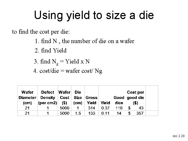
Using yield to size a die to find the cost per die: 1. find N , the number of die on a wafer 2. find Yield 3. find Ng = Yield x N 4. cost/die = wafer cost/ Ng soc 2. 20
Effect of defect density soc 2. 21
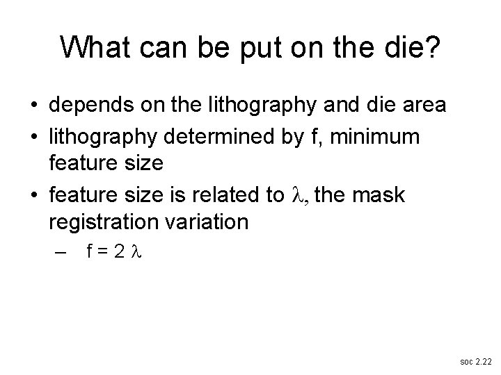
What can be put on the die? • depends on the lithography and die area • lithography determined by f, minimum feature size • feature size is related to the mask registration variation – f=2 soc 2. 22
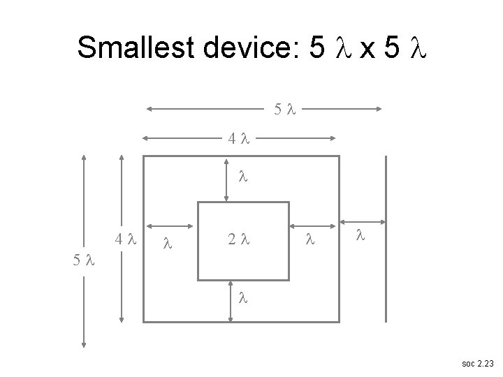
Smallest device: 5 x 5 5 4 4 5 2 soc 2. 23
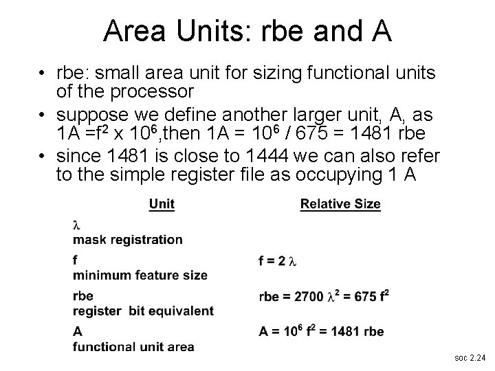
Area Units: rbe and A • rbe: small area unit for sizing functional units of the processor • suppose we define another larger unit, A, as 1 A =f 2 x 10⁶, then 1 A = 106 / 675 = 1481 rbe • since 1481 is close to 1444 we can also refer to the simple register file as occupying 1 A soc 2. 24
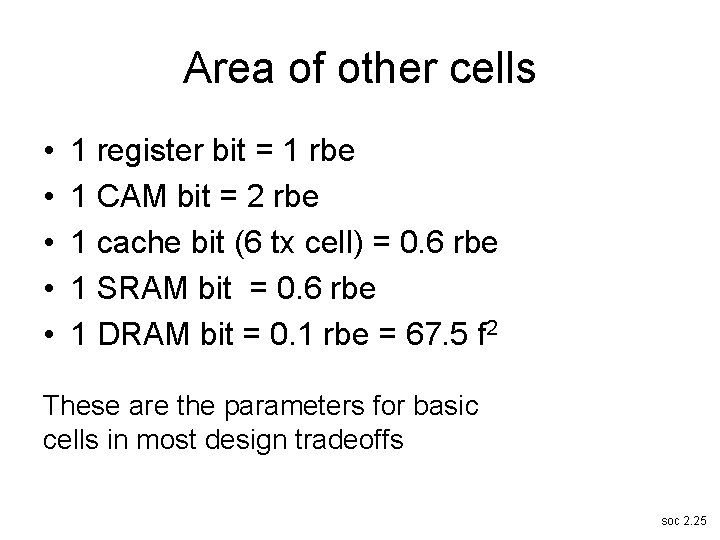
Area of other cells • • • 1 register bit = 1 rbe 1 CAM bit = 2 rbe 1 cache bit (6 tx cell) = 0. 6 rbe 1 SRAM bit = 0. 6 rbe 1 DRAM bit = 0. 1 rbe = 67. 5 f 2 These are the parameters for basic cells in most design tradeoffs soc 2. 25
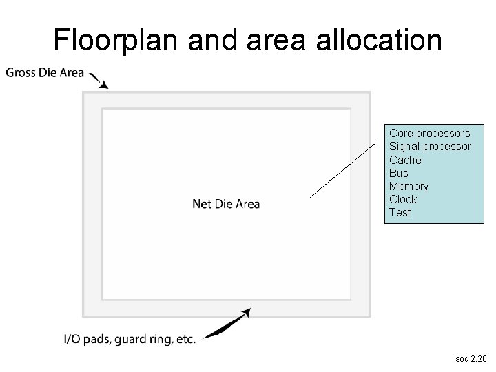
Floorplan and area allocation Core processors Signal processor Cache Bus Memory Clock Test soc 2. 26
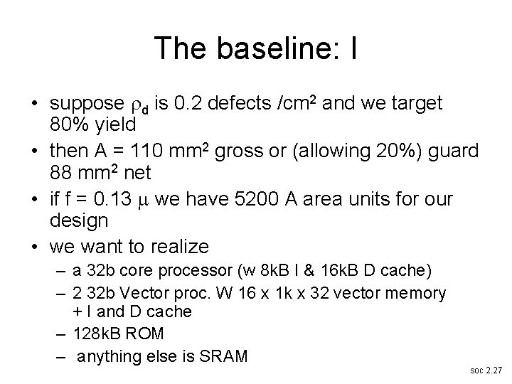
The baseline: I • suppose d is 0. 2 defects /cm 2 and we target 80% yield • then A = 110 mm 2 gross or (allowing 20%) guard 88 mm 2 net • if f = 0. 13 m we have 5200 A area units for our design • we want to realize – a 32 b core processor (w 8 k. B I & 16 k. B D cache) – 2 32 b Vector proc. W 16 x 1 k x 32 vector memory + I and D cache – 128 k. B ROM – anything else is SRAM soc 2. 27
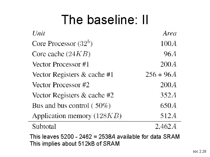
The baseline: II This leaves 5200 - 2462 = 2538 A available for data SRAM This implies about 512 k. B of SRAM soc 2. 28
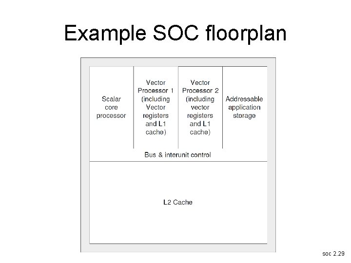
Example SOC floorplan soc 2. 29
Die area summary • cost: an exponential function of area • successful business model – targets initial production at relatively low yield (~0. 3) – ride learning curve and leverage technology to reduce cost and improve performance • technical innovation and analysis – intersect with business decisions to make a product – use design feasibility studies and empirical targets – methodology for cost and performance evaluation – marketing targets: determine weighting of performance metrics soc 2. 30
Power consumption • power consumption: becoming key design issue • increased power: largely due to higher frequency operation soc 2. 31
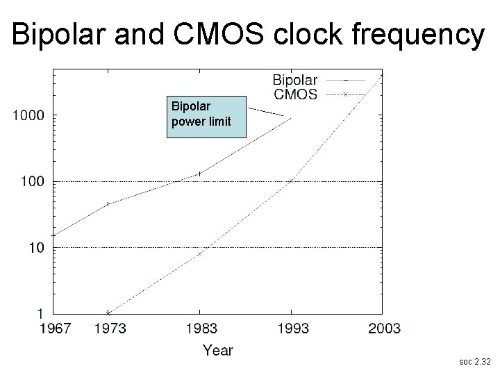
Bipolar and CMOS clock frequency Bipolar power limit soc 2. 32
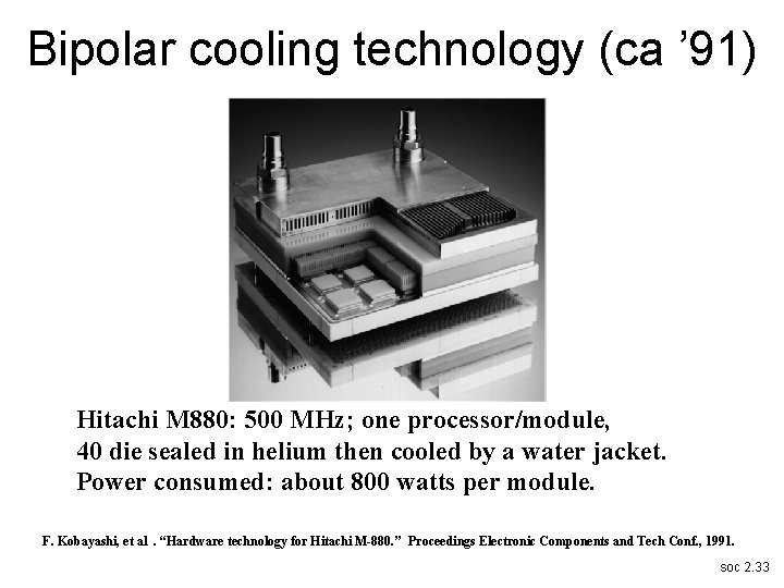
Bipolar cooling technology (ca ’ 91) Hitachi M 880: 500 MHz; one processor/module, 40 die sealed in helium then cooled by a water jacket. Power consumed: about 800 watts per module. F. Kobayashi, et al. “Hardware technology for Hitachi M-880. ” Proceedings Electronic Components and Tech Conf. , 1991. soc 2. 33
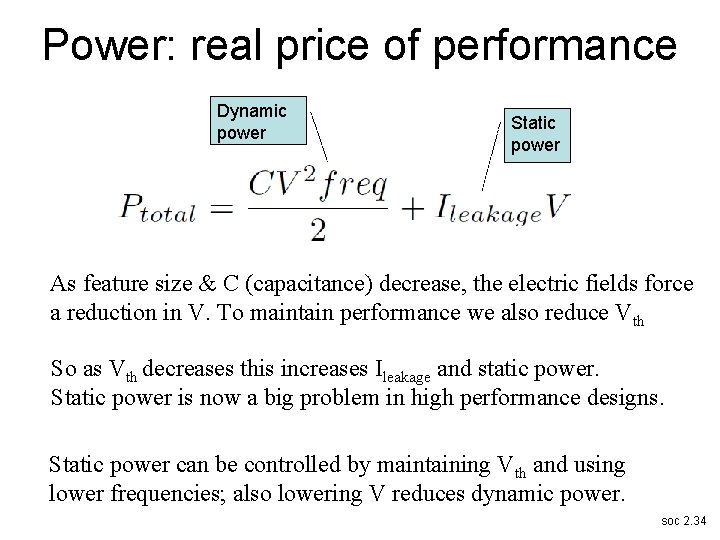
Power: real price of performance Dynamic power Static power As feature size & C (capacitance) decrease, the electric fields force a reduction in V. To maintain performance we also reduce Vth So as Vth decreases this increases Ileakage and static power. Static power is now a big problem in high performance designs. Static power can be controlled by maintaining Vth and using lower frequencies; also lowering V reduces dynamic power. soc 2. 34
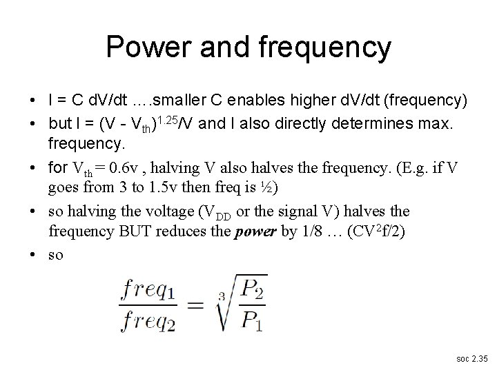
Power and frequency • I = C d. V/dt …. smaller C enables higher d. V/dt (frequency) • but I = (V - Vth)1. 25/V and I also directly determines max. frequency. • for Vth = 0. 6 v , halving V also halves the frequency. (E. g. if V goes from 3 to 1. 5 v then freq is ½) • so halving the voltage (VDD or the signal V) halves the frequency BUT reduces the power by 1/8 … (CV 2 f/2) • so soc 2. 35
Power: a new frontier • • cooled high power: >70 w/ die high power: 10 - 50 w/ die … plug in supply low power: 0. 1 - 2 w / die. . rechargeable battery very low power: 1 - 100 mw /die. . AA size batteries • extremely low power: 1 - 100 microwatt/die and below (nano watts). . button batteries • no power: extract from local EM field, …. O (1 uw/die) soc 2. 36
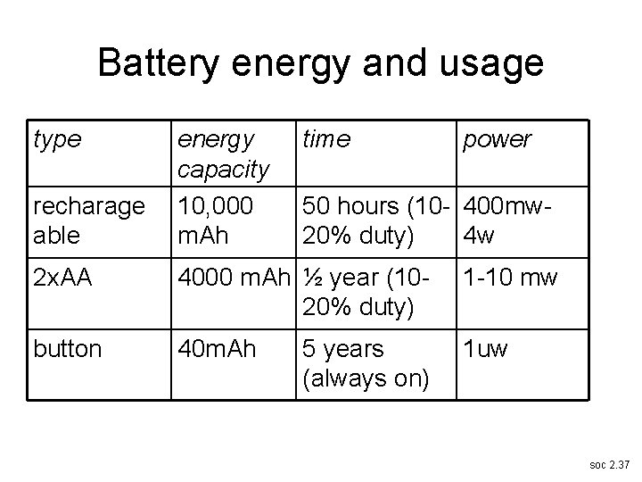
Battery energy and usage type recharage able energy capacity 10, 000 m. Ah time power 50 hours (10 - 400 mw 20% duty) 4 w 2 x. AA 4000 m. Ah ½ year (1020% duty) 1 -10 mw button 40 m. Ah 1 uw 5 years (always on) soc 2. 37
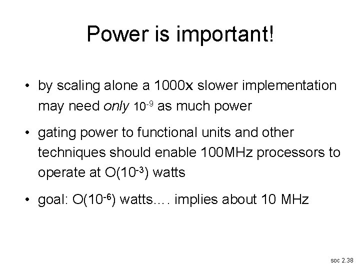
Power is important! • by scaling alone a 1000 x slower implementation may need only 10 -9 as much power • gating power to functional units and other techniques should enable 100 MHz processors to operate at O(10 -3) watts • goal: O(10 -6) watts…. implies about 10 MHz soc 2. 38
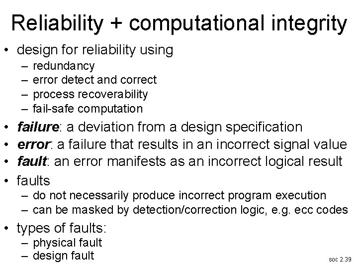
Reliability + computational integrity • design for reliability using – – • • redundancy error detect and correct process recoverability fail-safe computation failure: a deviation from a design specification error: a failure that results in an incorrect signal value fault: an error manifests as an incorrect logical result faults – do not necessarily produce incorrect program execution – can be masked by detection/correction logic, e. g. ecc codes • types of faults: – physical fault – design fault soc 2. 39
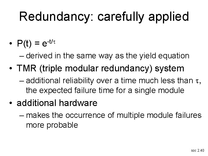
Redundancy: carefully applied • P(t) = e-t/t – derived in the same way as the yield equation • TMR (triple modular redundancy) system – additional reliability over a time much less than t the expected failure time for a single module • additional hardware – makes the occurrence of multiple module failures more probable soc 2. 40
Highly reliable designs • typical usage – error detection: parity, residue, block codes; sanity & bounds checks – action (instruction) retry – error correction: code or alternate path compute – reconfiguration soc 2. 41
Why reconfigurable design? • manage design complexity based on highperformance IP-blocks – avoid the risk and delay of fabrication • time – support highly-pipelined designs • area – regularity of FPGA, readily to advance to better process technology • reliability – FPGA enables redundant cells and interconnections, avoid run-time faults soc 2. 42
Area estimate of FPGAs • use rbe model as the basic measure – one slice 7000 transistors = 700 rbe – one logic element (LE) 12000 = 1200 rbe – Xilinx Virtex XC 2 V 6000 = 33, 792 slices • 23. 65 million rbe or 16400 A • 8 x 8 multiplier: around 35 slices – equivalent to 24500 rbe or 17 A – 1 -bit multiplier in VLSI contains a full-adder and an AND gate 3840 transistors = 384 rbe around 60 times smaller than reconfigurable version • block multipliers in FPGAs: more efficient soc 2. 43
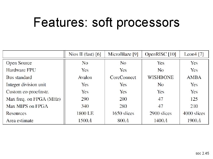
Soft processors: using FPGAs • soft processors how soft they are? – an instruction processor design in bit-stream format, used to program an FPGA device – cost reduction, design reuse, … • major soft processors include: – Altera: Nios – Xilinx: Micro. Blaze – open-source: Open. RISC, Leon – all 32 -bit RISC architecture with 5 -stage pipelines, connect to different bus standards soc 2. 44
Features: soft processors soc 2. 45
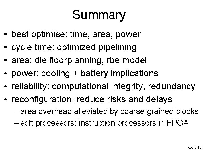
Summary • • • best optimise: time, area, power cycle time: optimized pipelining area: die floorplanning, rbe model power: cooling + battery implications reliability: computational integrity, redundancy reconfiguration: reduce risks and delays – area overhead alleviated by coarse-grained blocks – soft processors: instruction processors in FPGA soc 2. 46
- Slides: 46