Chapter 2 Basic Concepts in RF Design 2
Chapter 2 Basic Concepts in RF Design Ø Ø Ø Ø 2. 1 General Considerations 2. 2 Effects of Nonlinearity 2. 3 Noise 2. 4 Sensitivity and Dynamic Range 2. 5 Passive Impedance Transformation 2. 6 Scattering Parameters 2. 7 Analysis of Nonlinear Dynamic Systems 2. 8 Volterra Series Behzad Razavi, RF Microelectronics. 1 Prepared by Bo Wen, UCLA
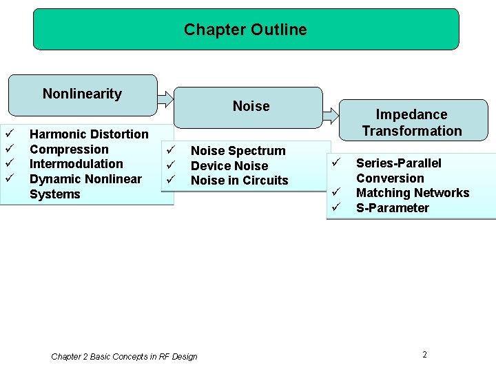
Chapter Outline Nonlinearity ü ü Harmonic Distortion Compression Intermodulation Dynamic Nonlinear Systems Noise ü ü ü Noise Spectrum Device Noise in Circuits Chapter 2 Basic Concepts in RF Design Impedance Transformation ü ü ü Series-Parallel Conversion Matching Networks S-Parameter 2
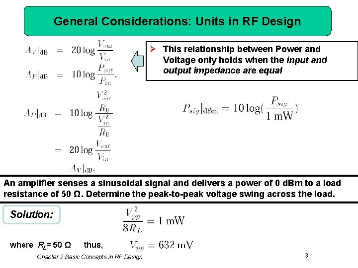
General Considerations: Units in RF Design Ø This relationship between Power and Voltage only holds when the input and output impedance are equal An amplifier senses a sinusoidal signal and delivers a power of 0 d. Bm to a load resistance of 50 Ω. Determine the peak-to-peak voltage swing across the load. Solution: where RL= 50 Ω thus, Chapter 2 Basic Concepts in RF Design 3
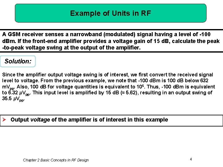
Example of Units in RF A GSM receiver senses a narrowband (modulated) signal having a level of -100 d. Bm. If the front-end amplifier provides a voltage gain of 15 d. B, calculate the peak -to-peak voltage swing at the output of the amplifier. Solution: Since the amplifier output voltage swing is of interest, we first convert the received signal level to voltage. From the previous example, we note that -100 d. Bm is 100 d. B below 632 m. Vpp. Also, 100 d. B for voltage quantities is equivalent to 105. Thus, -100 d. Bm is equivalent to 6. 32 μVpp. This input level is amplified by 15 d. B (≈ 5. 62), resulting in an output swing of 35. 5 μVpp. Ø Output voltage of the amplifier is of interest in this example Chapter 2 Basic Concepts in RF Design 4
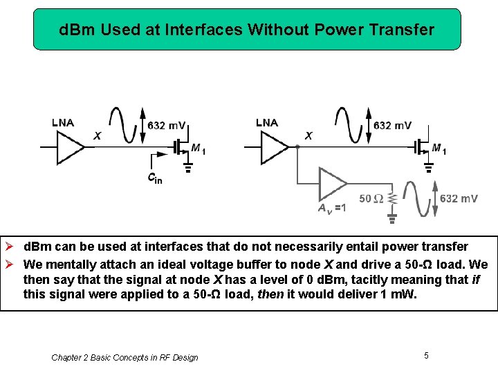
d. Bm Used at Interfaces Without Power Transfer Ø d. Bm can be used at interfaces that do not necessarily entail power transfer Ø We mentally attach an ideal voltage buffer to node X and drive a 50 -Ω load. We then say that the signal at node X has a level of 0 d. Bm, tacitly meaning that if this signal were applied to a 50 -Ω load, then it would deliver 1 m. W. Chapter 2 Basic Concepts in RF Design 5
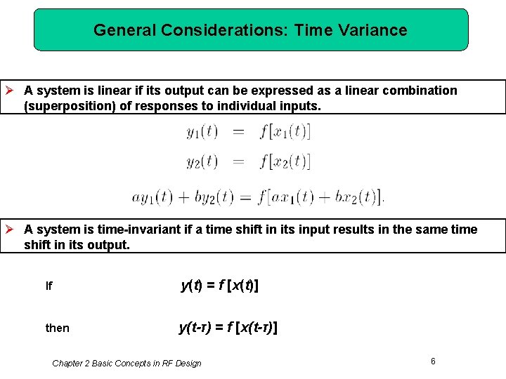
General Considerations: Time Variance Ø A system is linear if its output can be expressed as a linear combination (superposition) of responses to individual inputs. Ø A system is time-invariant if a time shift in its input results in the same time shift in its output. If y(t) = f [x(t)] then y(t-τ) = f [x(t-τ)] Chapter 2 Basic Concepts in RF Design 6
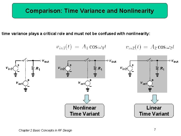
Comparison: Time Variance and Nonlinearity time variance plays a critical role and must not be confused with nonlinearity: Nonlinear Time Variant Chapter 2 Basic Concepts in RF Design Linear Time Variant 7

Example of Time Variance Plot the output waveform of the circuit above if vin 1 = A 1 cos ω1 t and vin 2 = A 2 cos(1. 25ω1 t). Solution: As shown above, vout tracks vin 2 if vin 1 > 0 and is pulled down to zero by R 1 if vin 1 < 0. That is, vout is equal to the product of vin 2 and a square wave toggling between 0 and 1. Chapter 2 Basic Concepts in RF Design 8
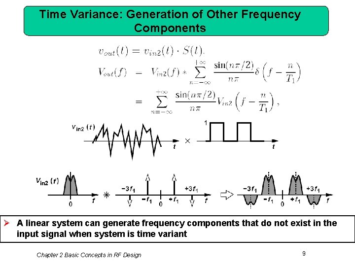
Time Variance: Generation of Other Frequency Components Ø A linear system can generate frequency components that do not exist in the input signal when system is time variant Chapter 2 Basic Concepts in RF Design 9

Nonlinearity: Memoryless and Static System linear nonlinear Ø The input/output characteristic of a memoryless nonlinear system can be approximated with a polynomial Ø In this idealized case, the circuit displays only second-order nonlinearity Chapter 2 Basic Concepts in RF Design 10
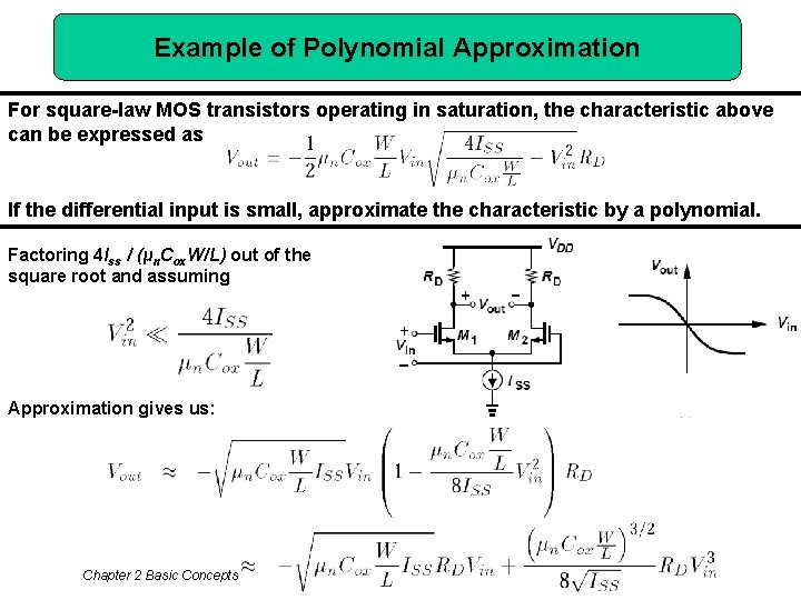
Example of Polynomial Approximation For square-law MOS transistors operating in saturation, the characteristic above can be expressed as If the differential input is small, approximate the characteristic by a polynomial. Factoring 4 Iss / (μn. Cox. W/L) out of the square root and assuming Approximation gives us: Chapter 2 Basic Concepts in RF Design 11
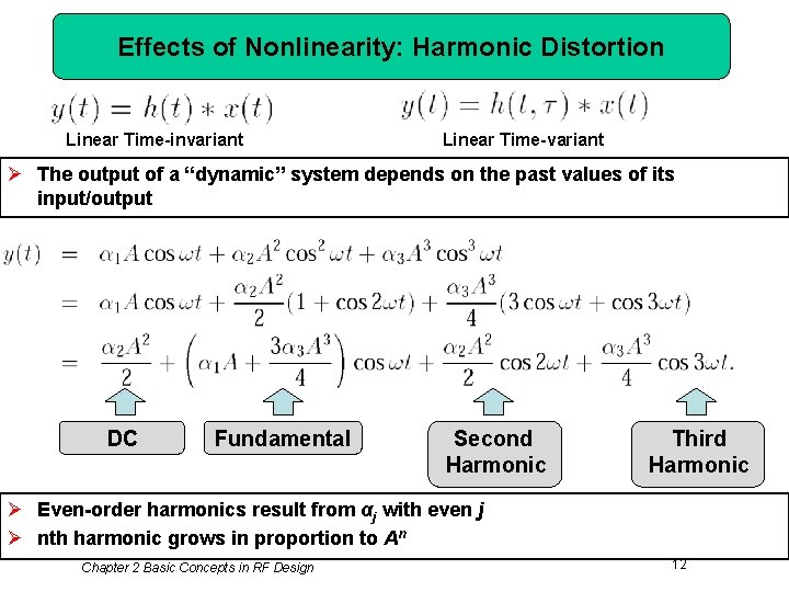
Effects of Nonlinearity: Harmonic Distortion Linear Time-invariant Linear Time-variant Ø The output of a “dynamic” system depends on the past values of its input/output DC Fundamental Second Harmonic Third Harmonic Ø Even-order harmonics result from αj with even j Ø nth harmonic grows in proportion to An Chapter 2 Basic Concepts in RF Design 12
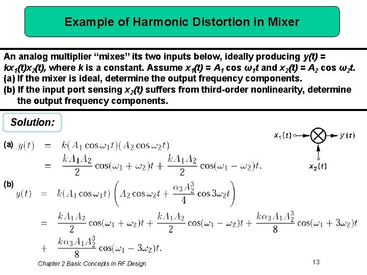
Example of Harmonic Distortion in Mixer An analog multiplier “mixes” its two inputs below, ideally producing y(t) = kx 1(t)x 2(t), where k is a constant. Assume x 1(t) = A 1 cos ω1 t and x 2(t) = A 2 cos ω2 t. (a) If the mixer is ideal, determine the output frequency components. (b) If the input port sensing x 2(t) suffers from third-order nonlinearity, determine the output frequency components. Solution: (a) (b) Chapter 2 Basic Concepts in RF Design 13
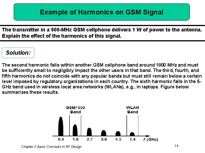
Example of Harmonics on GSM Signal The transmitter in a 900 -MHz GSM cellphone delivers 1 W of power to the antenna. Explain the effect of the harmonics of this signal. Solution: The second harmonic falls within another GSM cellphone band around 1800 MHz and must be sufficiently small to negligibly impact the other users in that band. The third, fourth, and fifth harmonics do not coincide with any popular bands but must still remain below a certain level imposed by regulatory organizations in each country. The sixth harmonic falls in the 5 GHz band used in wireless local area networks (WLANs), e. g. , in laptops. Figure below summarizes these results. Chapter 2 Basic Concepts in RF Design 14
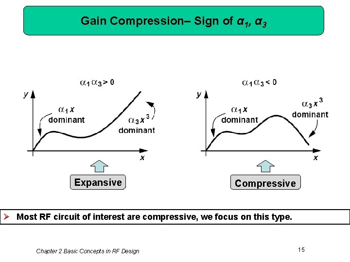
Gain Compression– Sign of α 1, α 3 Expansive Compressive Ø Most RF circuit of interest are compressive, we focus on this type. Chapter 2 Basic Concepts in RF Design 15
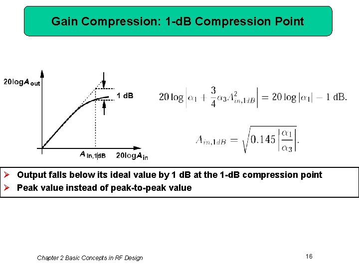
Gain Compression: 1 -d. B Compression Point Ø Output falls below its ideal value by 1 d. B at the 1 -d. B compression point Ø Peak value instead of peak-to-peak value Chapter 2 Basic Concepts in RF Design 16
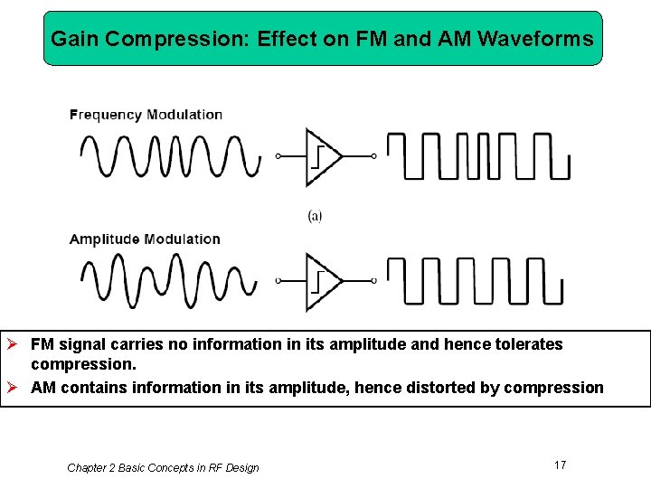
Gain Compression: Effect on FM and AM Waveforms Ø FM signal carries no information in its amplitude and hence tolerates compression. Ø AM contains information in its amplitude, hence distorted by compression Chapter 2 Basic Concepts in RF Design 17
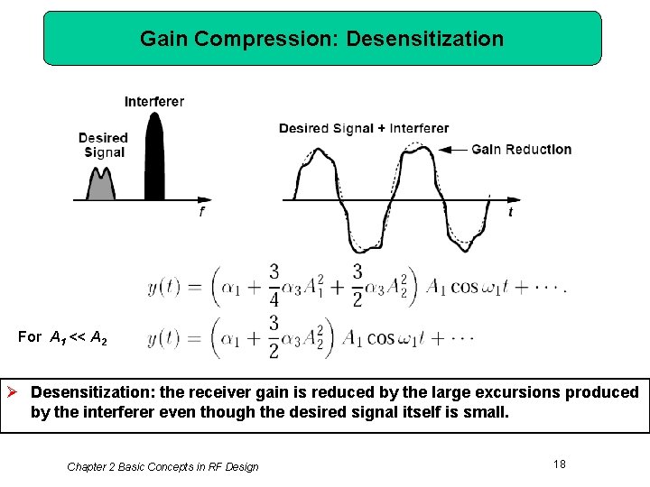
Gain Compression: Desensitization For A 1 << A 2 Ø Desensitization: the receiver gain is reduced by the large excursions produced by the interferer even though the desired signal itself is small. Chapter 2 Basic Concepts in RF Design 18
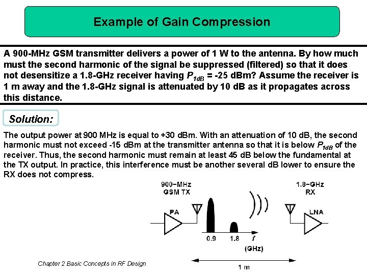
Example of Gain Compression A 900 -MHz GSM transmitter delivers a power of 1 W to the antenna. By how much must the second harmonic of the signal be suppressed (filtered) so that it does not desensitize a 1. 8 -GHz receiver having P 1 d. B = -25 d. Bm? Assume the receiver is 1 m away and the 1. 8 -GHz signal is attenuated by 10 d. B as it propagates across this distance. Solution: The output power at 900 MHz is equal to +30 d. Bm. With an attenuation of 10 d. B, the second harmonic must not exceed -15 d. Bm at the transmitter antenna so that it is below P 1 d. B of the receiver. Thus, the second harmonic must remain at least 45 d. B below the fundamental at the TX output. In practice, this interference must be another several d. B lower to ensure the RX does not compress. Chapter 2 Basic Concepts in RF Design 19
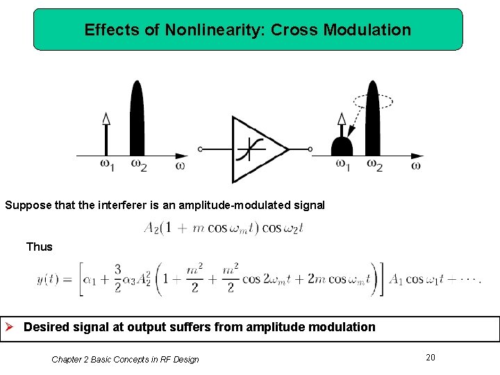
Effects of Nonlinearity: Cross Modulation Suppose that the interferer is an amplitude-modulated signal Thus Ø Desired signal at output suffers from amplitude modulation Chapter 2 Basic Concepts in RF Design 20
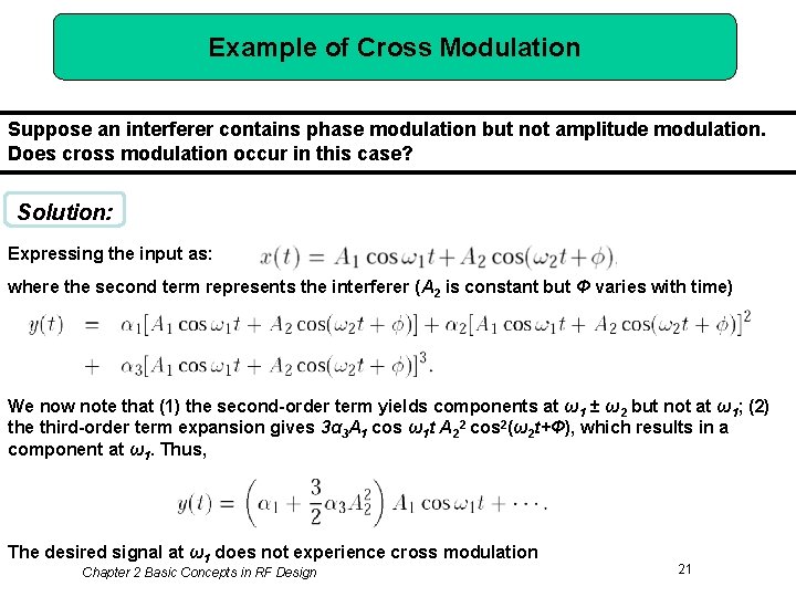
Example of Cross Modulation Suppose an interferer contains phase modulation but not amplitude modulation. Does cross modulation occur in this case? Solution: Expressing the input as: where the second term represents the interferer (A 2 is constant but Φ varies with time) We now note that (1) the second-order term yields components at ω1 ± ω2 but not at ω1; (2) the third-order term expansion gives 3α 3 A 1 cos ω1 t A 22 cos 2(ω2 t+Φ), which results in a component at ω1. Thus, The desired signal at ω1 does not experience cross modulation Chapter 2 Basic Concepts in RF Design 21
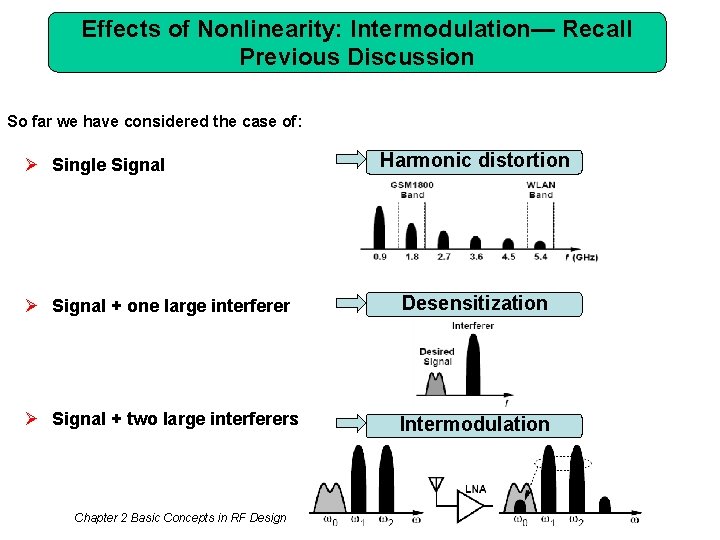
Effects of Nonlinearity: Intermodulation— Recall Previous Discussion So far we have considered the case of: Ø Single Signal Harmonic distortion Ø Signal + one large interferer Desensitization Ø Signal + two large interferers Intermodulation Chapter 2 Basic Concepts in RF Design 22
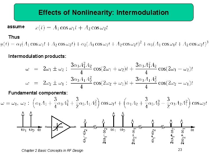
Effects of Nonlinearity: Intermodulation assume Thus Intermodulation products: Fundamental components: Chapter 2 Basic Concepts in RF Design 23
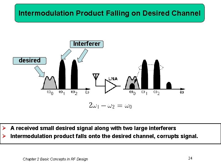
Intermodulation Product Falling on Desired Channel Interferer desired Ø A received small desired signal along with two large interferers Ø Intermodulation product falls onto the desired channel, corrupts signal. Chapter 2 Basic Concepts in RF Design 24
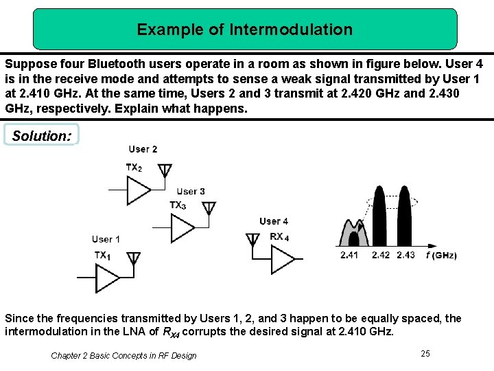
Example of Intermodulation Suppose four Bluetooth users operate in a room as shown in figure below. User 4 is in the receive mode and attempts to sense a weak signal transmitted by User 1 at 2. 410 GHz. At the same time, Users 2 and 3 transmit at 2. 420 GHz and 2. 430 GHz, respectively. Explain what happens. Solution: Since the frequencies transmitted by Users 1, 2, and 3 happen to be equally spaced, the intermodulation in the LNA of RX 4 corrupts the desired signal at 2. 410 GHz. Chapter 2 Basic Concepts in RF Design 25
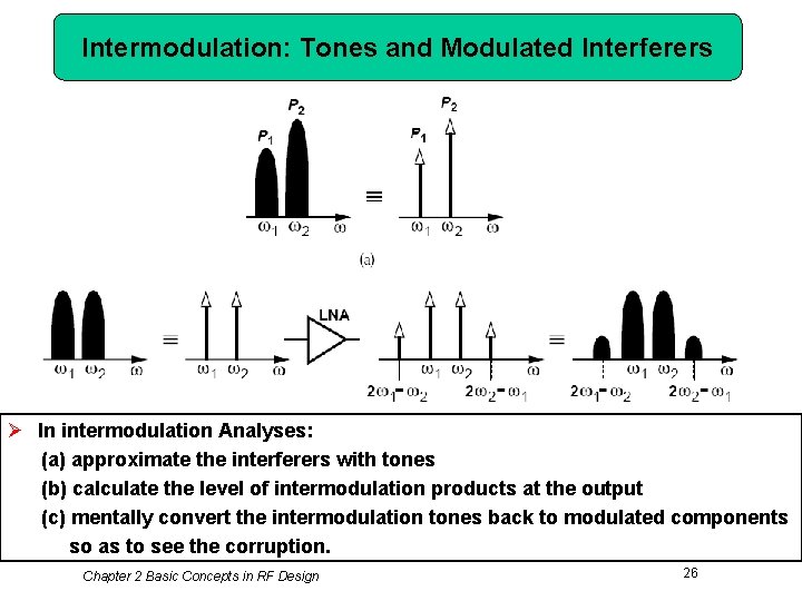
Intermodulation: Tones and Modulated Interferers Ø In intermodulation Analyses: (a) approximate the interferers with tones (b) calculate the level of intermodulation products at the output (c) mentally convert the intermodulation tones back to modulated components so as to see the corruption. Chapter 2 Basic Concepts in RF Design 26
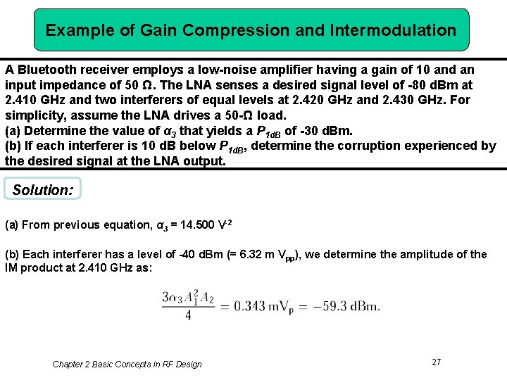
Example of Gain Compression and Intermodulation A Bluetooth receiver employs a low-noise amplifier having a gain of 10 and an input impedance of 50 Ω. The LNA senses a desired signal level of -80 d. Bm at 2. 410 GHz and two interferers of equal levels at 2. 420 GHz and 2. 430 GHz. For simplicity, assume the LNA drives a 50 -Ω load. (a) Determine the value of α 3 that yields a P 1 d. B of -30 d. Bm. (b) If each interferer is 10 d. B below P 1 d. B, determine the corruption experienced by the desired signal at the LNA output. Solution: (a) From previous equation, α 3 = 14. 500 V-2 (b) Each interferer has a level of -40 d. Bm (= 6. 32 m Vpp), we determine the amplitude of the IM product at 2. 410 GHz as: Chapter 2 Basic Concepts in RF Design 27
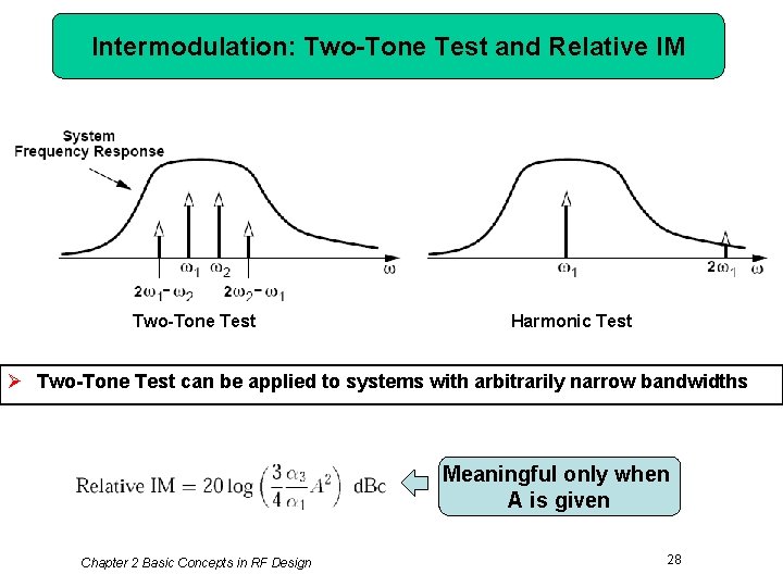
Intermodulation: Two-Tone Test and Relative IM Two-Tone Test Harmonic Test Ø Two-Tone Test can be applied to systems with arbitrarily narrow bandwidths Meaningful only when A is given Chapter 2 Basic Concepts in RF Design 28
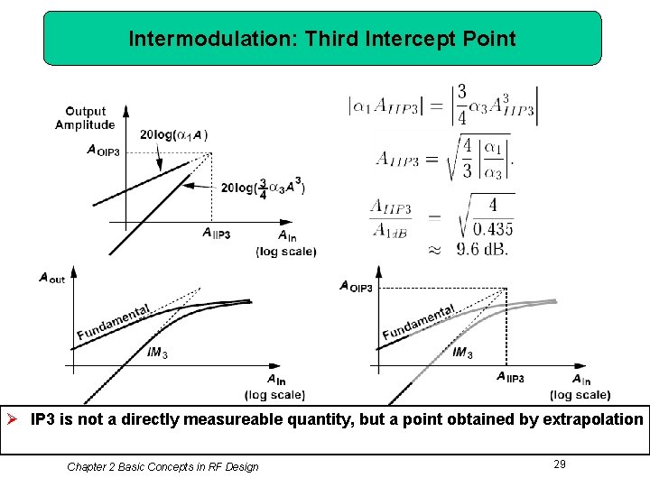
Intermodulation: Third Intercept Point Ø IP 3 is not a directly measureable quantity, but a point obtained by extrapolation Chapter 2 Basic Concepts in RF Design 29
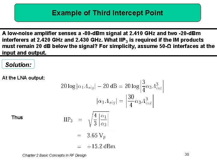
Example of Third Intercept Point A low-noise amplifier senses a -80 -d. Bm signal at 2. 410 GHz and two -20 -d. Bm interferers at 2. 420 GHz and 2. 430 GHz. What IIP 3 is required if the IM products must remain 20 d. B below the signal? For simplicity, assume 50 -Ω interfaces at the input and output. Solution: At the LNA output: Thus Chapter 2 Basic Concepts in RF Design 30
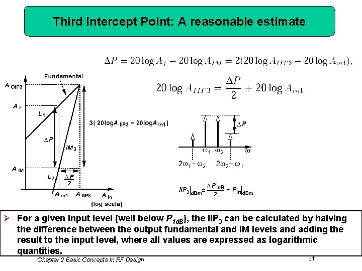
Third Intercept Point: A reasonable estimate Ø For a given input level (well below P 1 d. B), the IIP 3 can be calculated by halving the difference between the output fundamental and IM levels and adding the result to the input level, where all values are expressed as logarithmic quantities. Chapter 2 Basic Concepts in RF Design 31
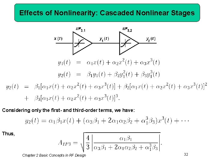
Effects of Nonlinearity: Cascaded Nonlinear Stages Considering only the first- and third-order terms, we have: Thus, Chapter 2 Basic Concepts in RF Design 32
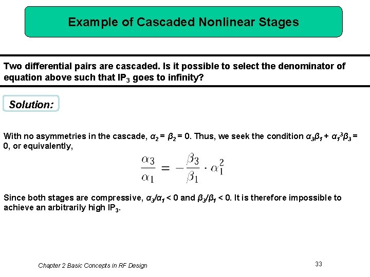
Example of Cascaded Nonlinear Stages Two differential pairs are cascaded. Is it possible to select the denominator of equation above such that IP 3 goes to infinity? Solution: With no asymmetries in the cascade, α 2 = β 2 = 0. Thus, we seek the condition α 3β 1 + α 13β 3 = 0, or equivalently, Since both stages are compressive, α 3/α 1 < 0 and β 3/β 1 < 0. It is therefore impossible to achieve an arbitrarily high IP 3. Chapter 2 Basic Concepts in RF Design 33
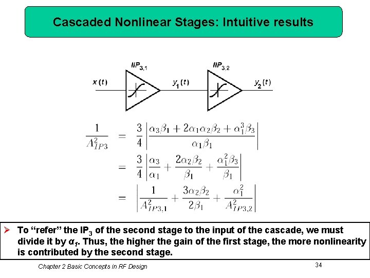
Cascaded Nonlinear Stages: Intuitive results Ø To “refer” the IP 3 of the second stage to the input of the cascade, we must divide it by α 1. Thus, the higher the gain of the first stage, the more nonlinearity is contributed by the second stage. Chapter 2 Basic Concepts in RF Design 34
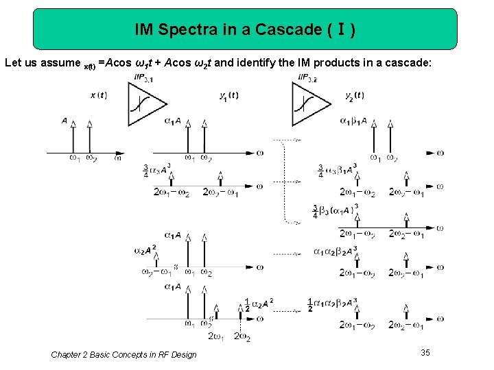
IM Spectra in a Cascade (Ⅰ) Let us assume x(t) =Acos ω1 t + Acos ω2 t and identify the IM products in a cascade: Chapter 2 Basic Concepts in RF Design 35
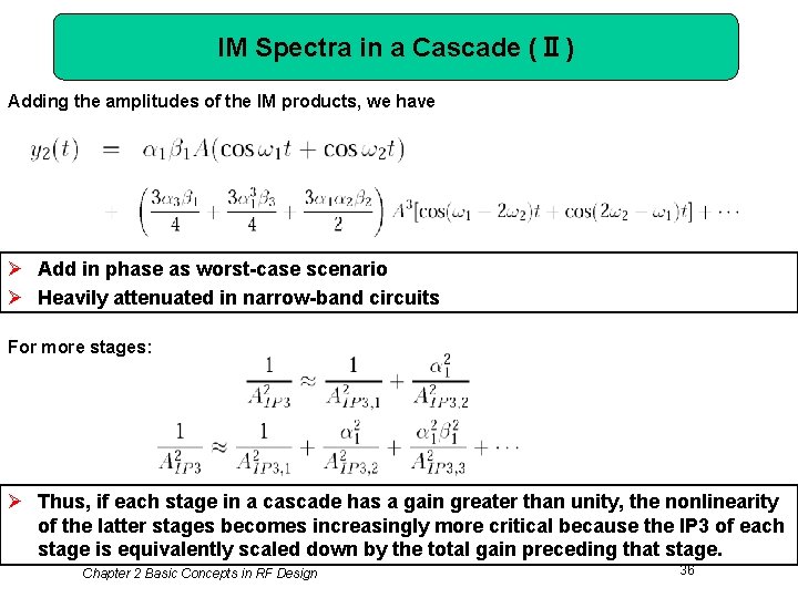
IM Spectra in a Cascade (Ⅱ) Adding the amplitudes of the IM products, we have Ø Add in phase as worst-case scenario Ø Heavily attenuated in narrow-band circuits For more stages: Ø Thus, if each stage in a cascade has a gain greater than unity, the nonlinearity of the latter stages becomes increasingly more critical because the IP 3 of each stage is equivalently scaled down by the total gain preceding that stage. Chapter 2 Basic Concepts in RF Design 36
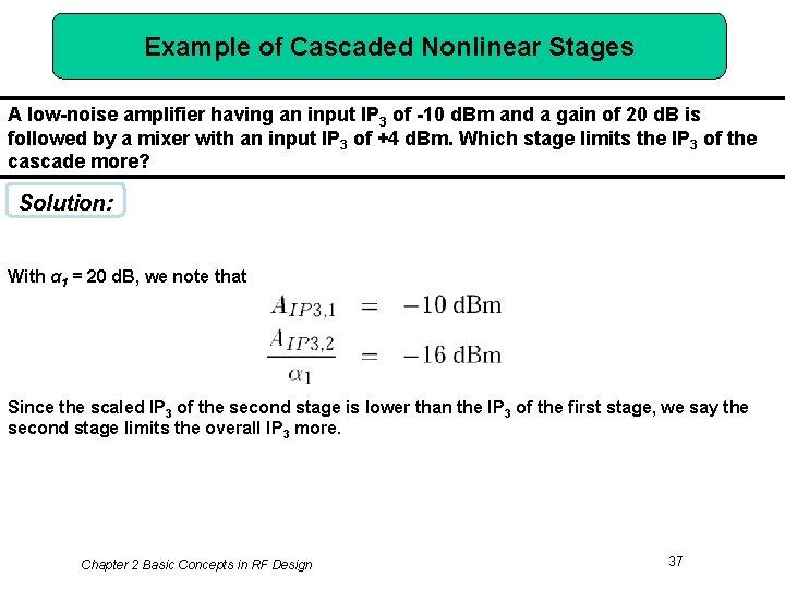
Example of Cascaded Nonlinear Stages A low-noise amplifier having an input IP 3 of -10 d. Bm and a gain of 20 d. B is followed by a mixer with an input IP 3 of +4 d. Bm. Which stage limits the IP 3 of the cascade more? Solution: With α 1 = 20 d. B, we note that Since the scaled IP 3 of the second stage is lower than the IP 3 of the first stage, we say the second stage limits the overall IP 3 more. Chapter 2 Basic Concepts in RF Design 37
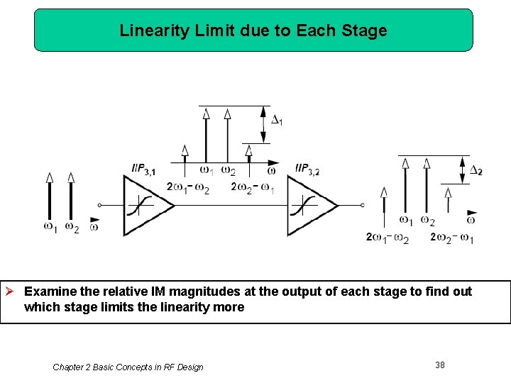
Linearity Limit due to Each Stage Ø Examine the relative IM magnitudes at the output of each stage to find out which stage limits the linearity more Chapter 2 Basic Concepts in RF Design 38
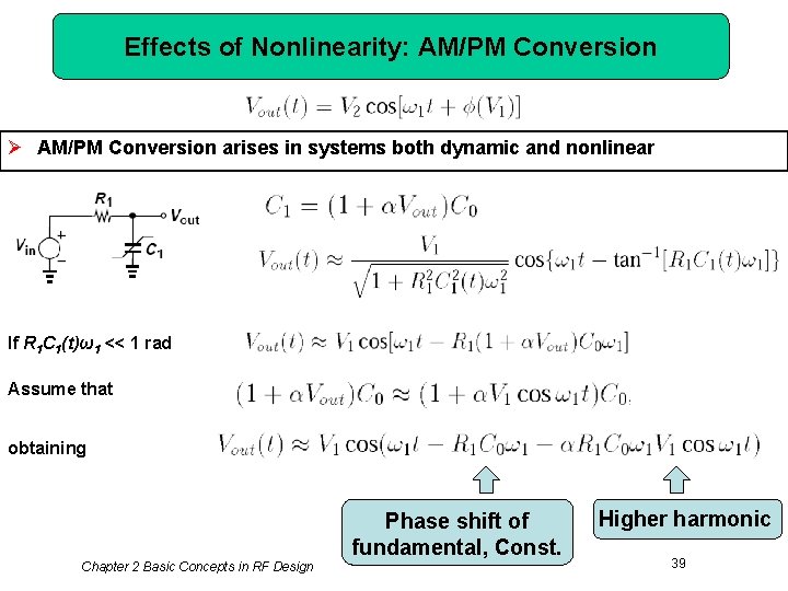
Effects of Nonlinearity: AM/PM Conversion Ø AM/PM Conversion arises in systems both dynamic and nonlinear If R 1 C 1(t)ω1 << 1 rad Assume that obtaining Chapter 2 Basic Concepts in RF Design Phase shift of fundamental, Const. Higher harmonic 39
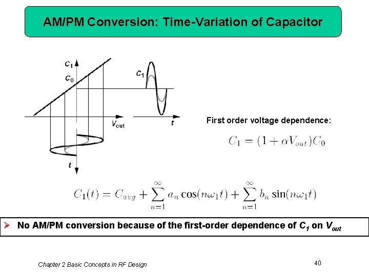
AM/PM Conversion: Time-Variation of Capacitor First order voltage dependence: Ø No AM/PM conversion because of the first-order dependence of C 1 on Vout Chapter 2 Basic Concepts in RF Design 40
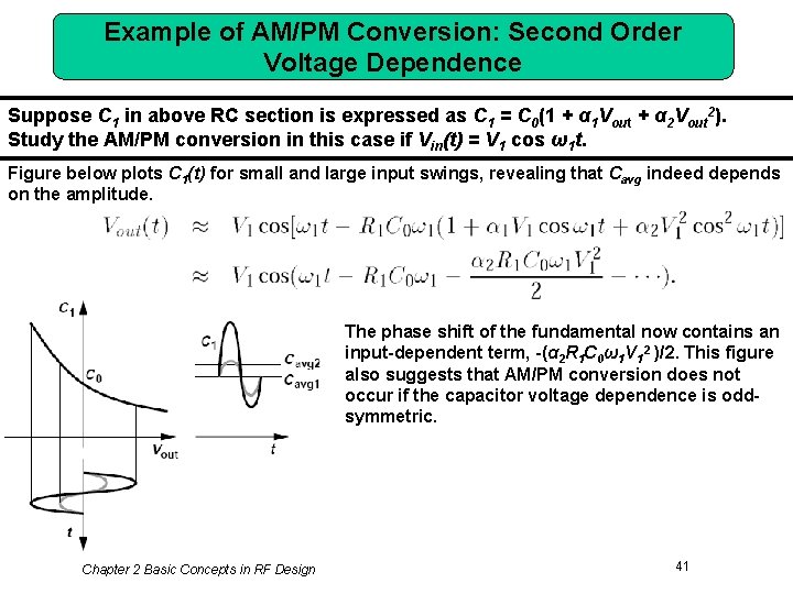
Example of AM/PM Conversion: Second Order Voltage Dependence Suppose C 1 in above RC section is expressed as C 1 = C 0(1 + α 1 Vout + α 2 Vout 2). Study the AM/PM conversion in this case if Vin(t) = V 1 cos ω1 t. Figure below plots C 1(t) for small and large input swings, revealing that Cavg indeed depends on the amplitude. The phase shift of the fundamental now contains an input-dependent term, -(α 2 R 1 C 0ω1 V 12 )/2. This figure also suggests that AM/PM conversion does not occur if the capacitor voltage dependence is oddsymmetric. Chapter 2 Basic Concepts in RF Design 41
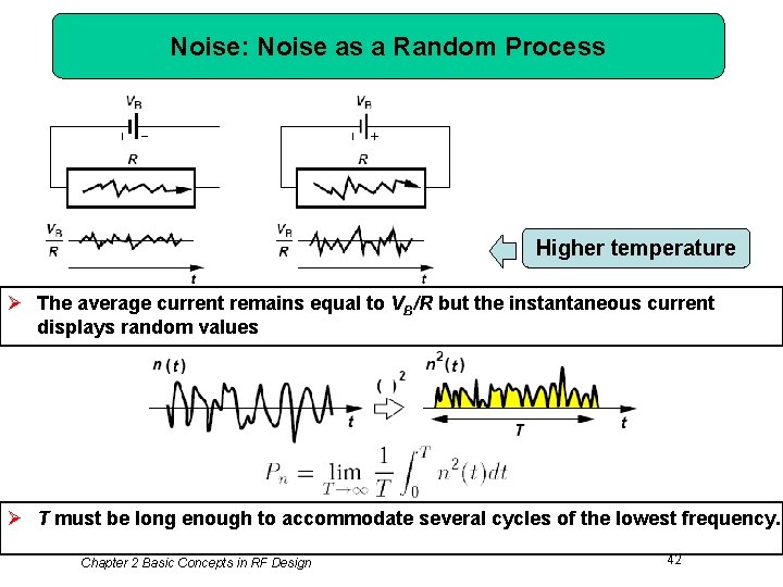
Noise: Noise as a Random Process Higher temperature Ø The average current remains equal to VB/R but the instantaneous current displays random values Ø T must be long enough to accommodate several cycles of the lowest frequency. Chapter 2 Basic Concepts in RF Design 42
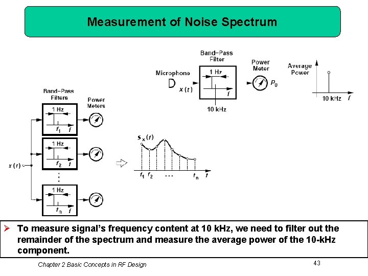
Measurement of Noise Spectrum Ø To measure signal’s frequency content at 10 k. Hz, we need to filter out the remainder of the spectrum and measure the average power of the 10 -k. Hz component. Chapter 2 Basic Concepts in RF Design 43
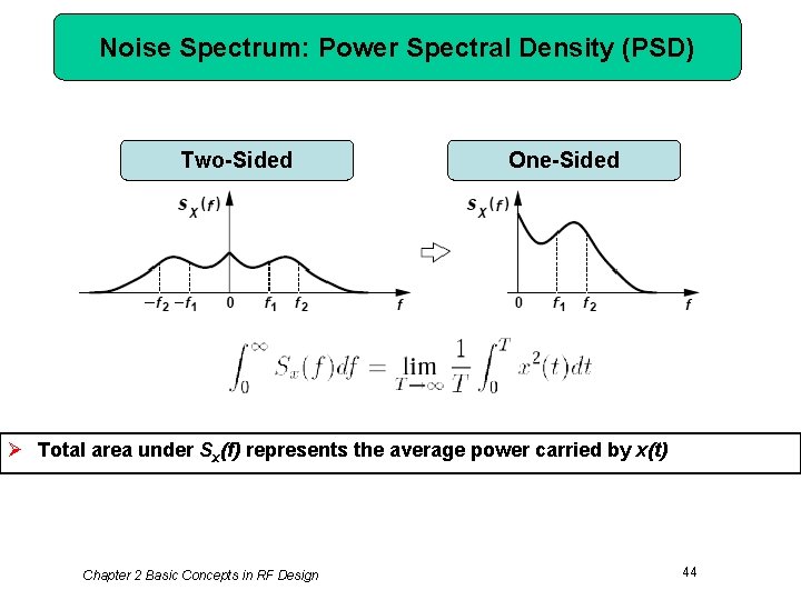
Noise Spectrum: Power Spectral Density (PSD) Two-Sided One-Sided Ø Total area under Sx(f) represents the average power carried by x(t) Chapter 2 Basic Concepts in RF Design 44
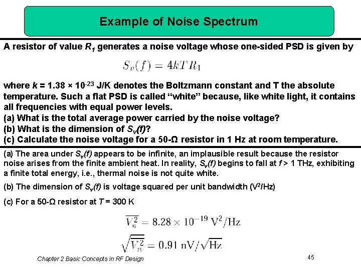
Example of Noise Spectrum A resistor of value R 1 generates a noise voltage whose one-sided PSD is given by where k = 1. 38 × 10 -23 J/K denotes the Boltzmann constant and T the absolute temperature. Such a flat PSD is called “white” because, like white light, it contains all frequencies with equal power levels. (a) What is the total average power carried by the noise voltage? (b) What is the dimension of Sv(f)? (c) Calculate the noise voltage for a 50 -Ω resistor in 1 Hz at room temperature. (a) The area under Sv(f) appears to be infinite, an implausible result because the resistor noise arises from the finite ambient heat. In reality, Sv(f) begins to fall at f > 1 THz, exhibiting a finite total energy, i. e. , thermal noise is not quite white. (b) The dimension of Sv(f) is voltage squared per unit bandwidth (V 2/Hz) (c) For a 50 -Ω resistor at T = 300 K Chapter 2 Basic Concepts in RF Design 45
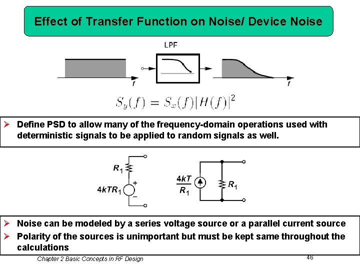
Effect of Transfer Function on Noise/ Device Noise Ø Define PSD to allow many of the frequency-domain operations used with deterministic signals to be applied to random signals as well. Ø Noise can be modeled by a series voltage source or a parallel current source Ø Polarity of the sources is unimportant but must be kept same throughout the calculations Chapter 2 Basic Concepts in RF Design 46
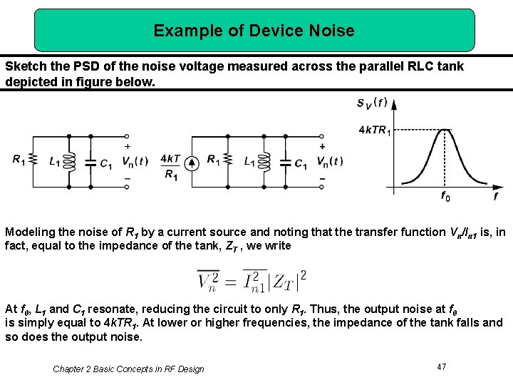
Example of Device Noise Sketch the PSD of the noise voltage measured across the parallel RLC tank depicted in figure below. Modeling the noise of R 1 by a current source and noting that the transfer function Vn/In 1 is, in fact, equal to the impedance of the tank, ZT , we write At f 0, L 1 and C 1 resonate, reducing the circuit to only R 1. Thus, the output noise at f 0 is simply equal to 4 k. TR 1. At lower or higher frequencies, the impedance of the tank falls and so does the output noise. Chapter 2 Basic Concepts in RF Design 47
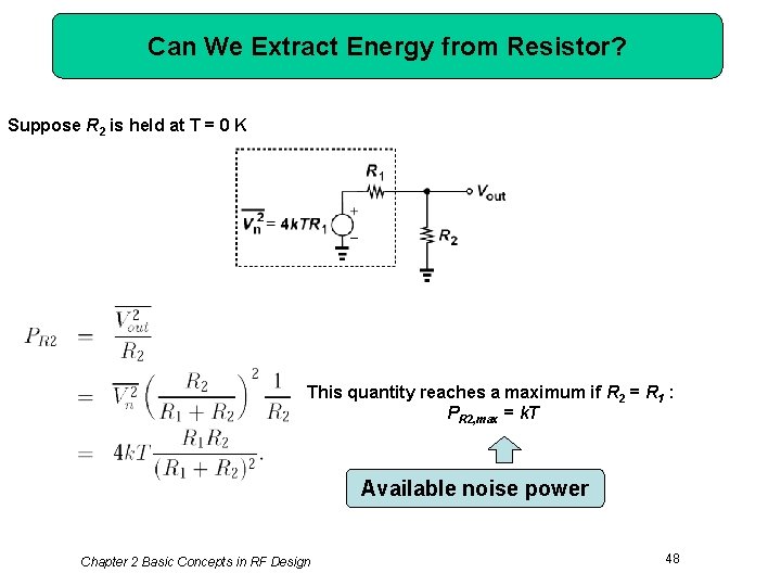
Can We Extract Energy from Resistor? Suppose R 2 is held at T = 0 K This quantity reaches a maximum if R 2 = R 1 : PR 2, max = k. T Available noise power Chapter 2 Basic Concepts in RF Design 48
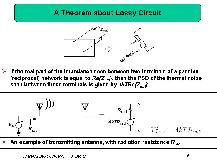
A Theorem about Lossy Circuit Ø If the real part of the impedance seen between two terminals of a passive (reciprocal) network is equal to Re{Zout}, then the PSD of thermal noise seen between these terminals is given by 4 k. TRe{Zout} Ø An example of transmitting antenna, with radiation resistance Rrad Chapter 2 Basic Concepts in RF Design 49
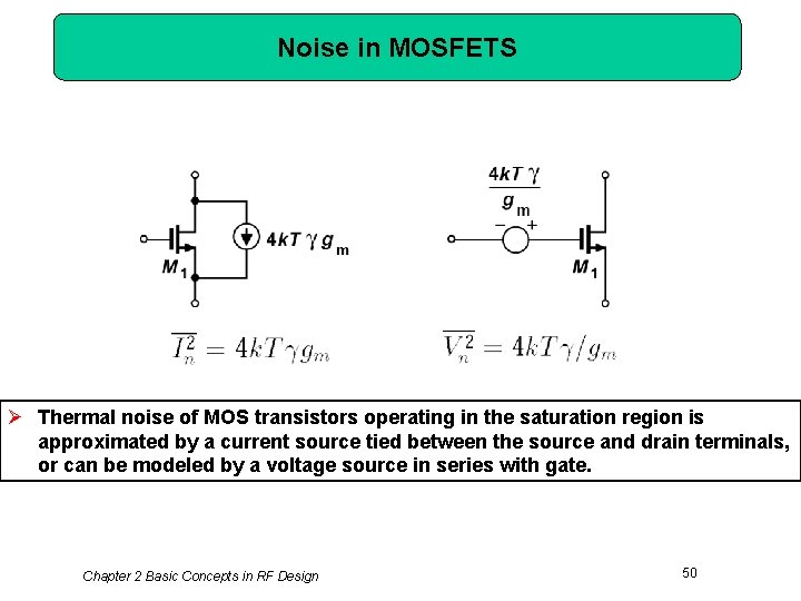
Noise in MOSFETS Ø Thermal noise of MOS transistors operating in the saturation region is approximated by a current source tied between the source and drain terminals, or can be modeled by a voltage source in series with gate. Chapter 2 Basic Concepts in RF Design 50
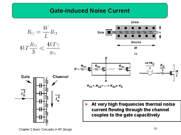
Gate-induced Noise Current Ø At very high frequencies thermal noise current flowing through the channel couples to the gate capacitively Chapter 2 Basic Concepts in RF Design 51
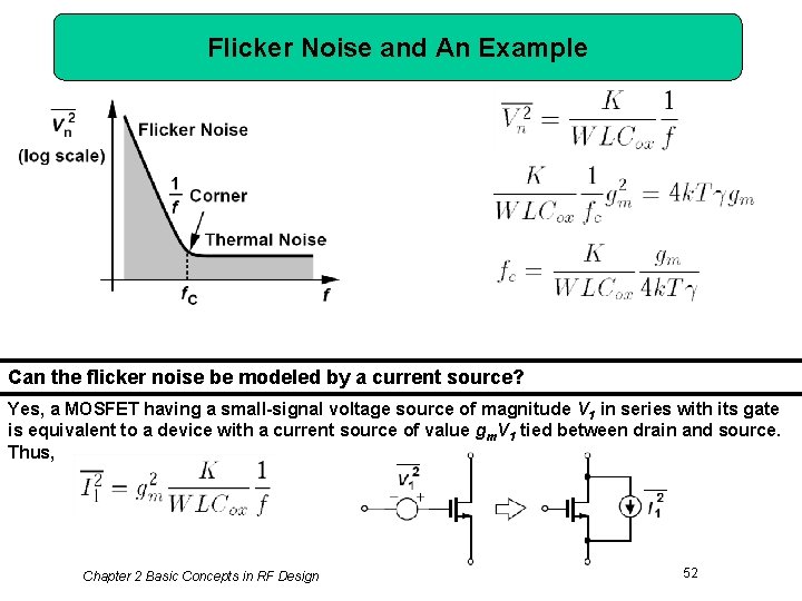
Flicker Noise and An Example Can the flicker noise be modeled by a current source? Yes, a MOSFET having a small-signal voltage source of magnitude V 1 in series with its gate is equivalent to a device with a current source of value gm. V 1 tied between drain and source. Thus, Chapter 2 Basic Concepts in RF Design 52
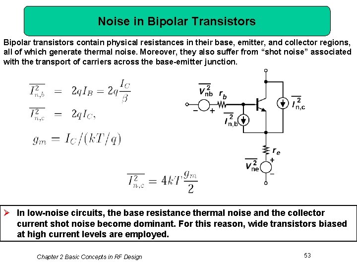
Noise in Bipolar Transistors Bipolar transistors contain physical resistances in their base, emitter, and collector regions, all of which generate thermal noise. Moreover, they also suffer from “shot noise” associated with the transport of carriers across the base-emitter junction. Ø In low-noise circuits, the base resistance thermal noise and the collector current shot noise become dominant. For this reason, wide transistors biased at high current levels are employed. Chapter 2 Basic Concepts in RF Design 53
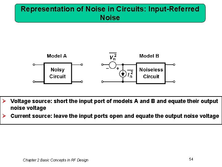
Representation of Noise in Circuits: Input-Referred Noise Ø Voltage source: short the input port of models A and B and equate their output noise voltage Ø Current source: leave the input ports open and equate the output noise voltage Chapter 2 Basic Concepts in RF Design 54
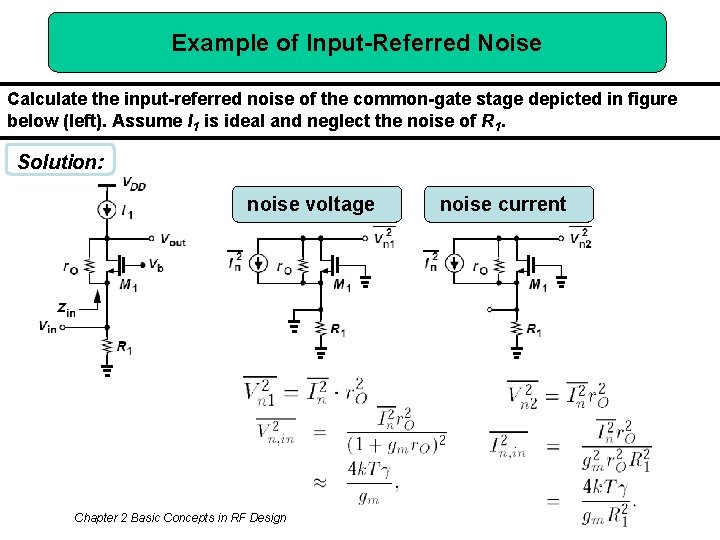
Example of Input-Referred Noise Calculate the input-referred noise of the common-gate stage depicted in figure below (left). Assume I 1 is ideal and neglect the noise of R 1. Solution: noise voltage Chapter 2 Basic Concepts in RF Design noise current 55
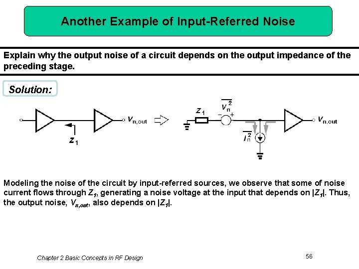
Another Example of Input-Referred Noise Explain why the output noise of a circuit depends on the output impedance of the preceding stage. Solution: Modeling the noise of the circuit by input-referred sources, we observe that some of noise current flows through Z 1, generating a noise voltage at the input that depends on |Z 1|. Thus, the output noise, Vn, out, also depends on |Z 1|. Chapter 2 Basic Concepts in RF Design 56
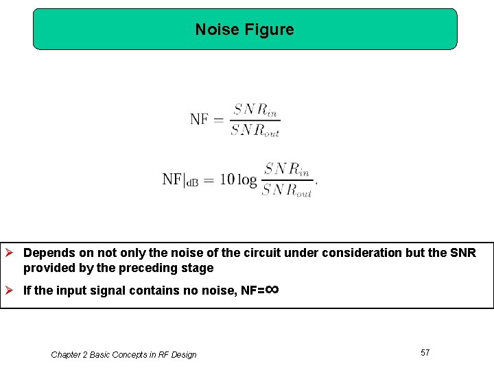
Noise Figure Ø Depends on not only the noise of the circuit under consideration but the SNR provided by the preceding stage Ø If the input signal contains no noise, NF=∞ Chapter 2 Basic Concepts in RF Design 57
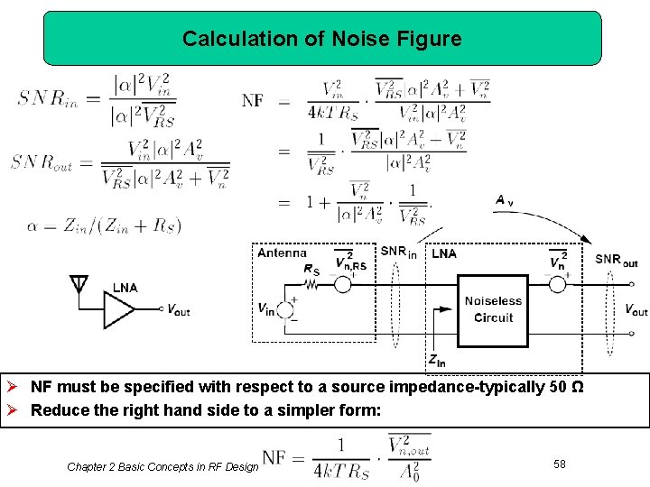
Calculation of Noise Figure Ø NF must be specified with respect to a source impedance-typically 50 Ω Ø Reduce the right hand side to a simpler form: Chapter 2 Basic Concepts in RF Design 58
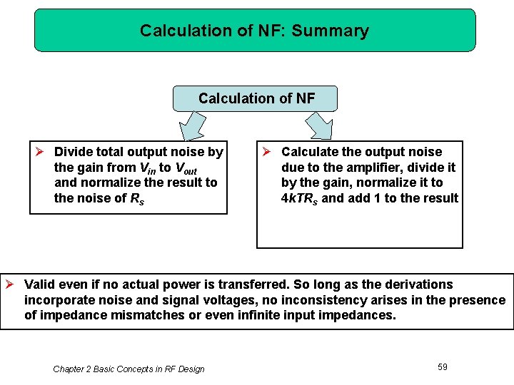
Calculation of NF: Summary Calculation of NF Ø Divide total output noise by the gain from Vin to Vout and normalize the result to the noise of Rs Ø Calculate the output noise due to the amplifier, divide it by the gain, normalize it to 4 k. TRs and add 1 to the result Ø Valid even if no actual power is transferred. So long as the derivations incorporate noise and signal voltages, no inconsistency arises in the presence of impedance mismatches or even infinite input impedances. Chapter 2 Basic Concepts in RF Design 59
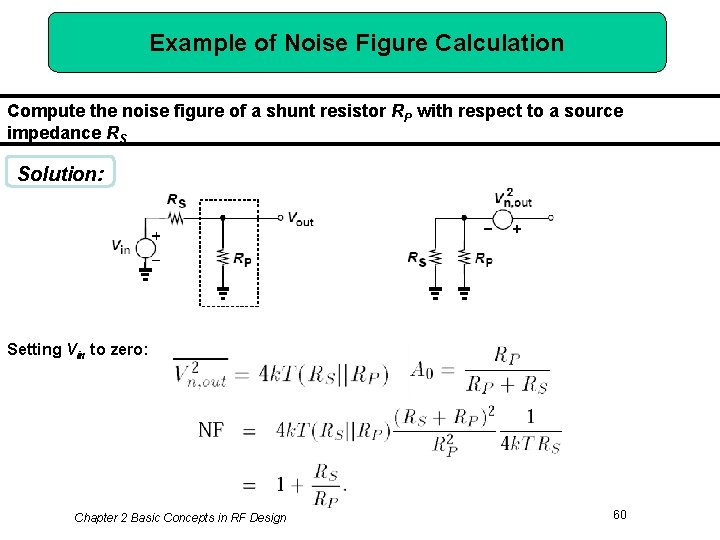
Example of Noise Figure Calculation Compute the noise figure of a shunt resistor RP with respect to a source impedance RS Solution: Setting Vin to zero: Chapter 2 Basic Concepts in RF Design 60
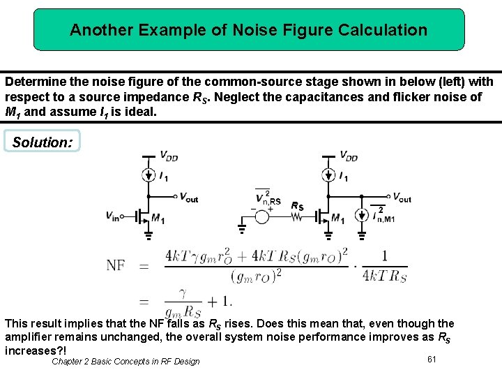
Another Example of Noise Figure Calculation Determine the noise figure of the common-source stage shown in below (left) with respect to a source impedance RS. Neglect the capacitances and flicker noise of M 1 and assume I 1 is ideal. Solution: This result implies that the NF falls as RS rises. Does this mean that, even though the amplifier remains unchanged, the overall system noise performance improves as RS increases? ! Chapter 2 Basic Concepts in RF Design 61
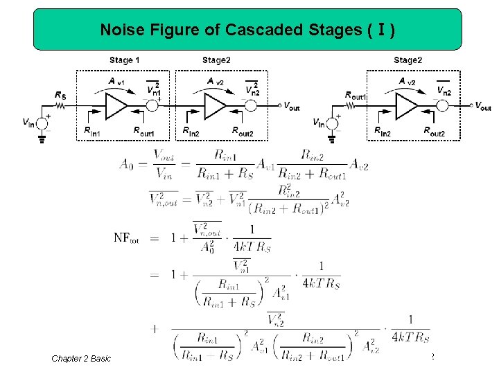
Noise Figure of Cascaded Stages (Ⅰ) Chapter 2 Basic Concepts in RF Design 62
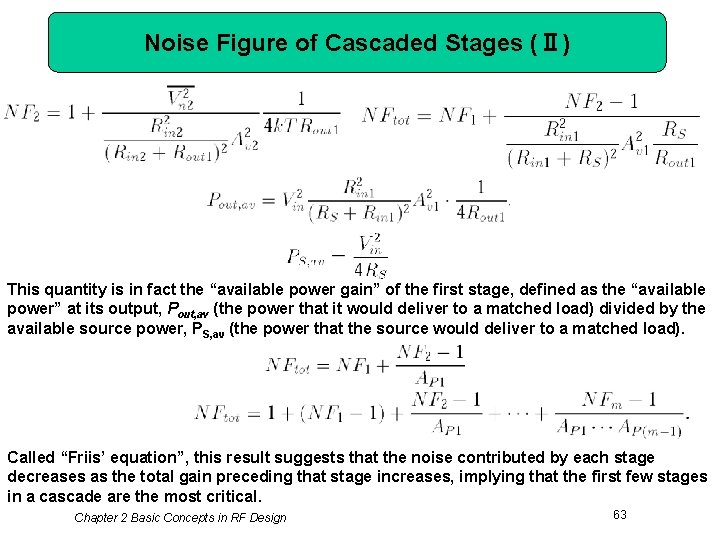
Noise Figure of Cascaded Stages (Ⅱ) This quantity is in fact the “available power gain” of the first stage, defined as the “available power” at its output, Pout, av (the power that it would deliver to a matched load) divided by the available source power, PS, av (the power that the source would deliver to a matched load). Called “Friis’ equation”, this result suggests that the noise contributed by each stage decreases as the total gain preceding that stage increases, implying that the first few stages in a cascade are the most critical. Chapter 2 Basic Concepts in RF Design 63
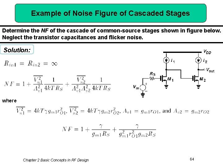
Example of Noise Figure of Cascaded Stages Determine the NF of the cascade of common-source stages shown in figure below. Neglect the transistor capacitances and flicker noise. Solution: where Chapter 2 Basic Concepts in RF Design 64
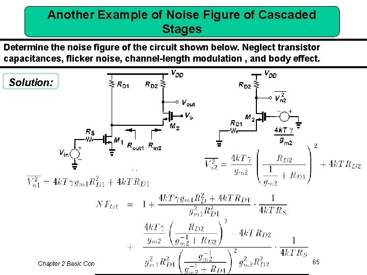
Another Example of Noise Figure of Cascaded Stages Determine the noise figure of the circuit shown below. Neglect transistor capacitances, flicker noise, channel-length modulation , and body effect. Solution: Chapter 2 Basic Concepts in RF Design 65
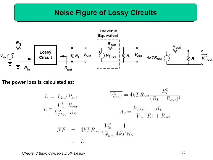
Noise Figure of Lossy Circuits The power loss is calculated as: Chapter 2 Basic Concepts in RF Design 66
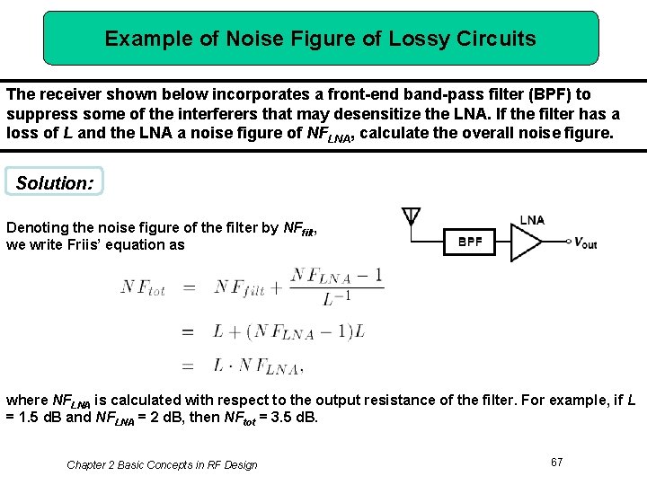
Example of Noise Figure of Lossy Circuits The receiver shown below incorporates a front-end band-pass filter (BPF) to suppress some of the interferers that may desensitize the LNA. If the filter has a loss of L and the LNA a noise figure of NFLNA, calculate the overall noise figure. Solution: Denoting the noise figure of the filter by NFfilt, we write Friis’ equation as where NFLNA is calculated with respect to the output resistance of the filter. For example, if L = 1. 5 d. B and NFLNA = 2 d. B, then NFtot = 3. 5 d. B. Chapter 2 Basic Concepts in RF Design 67
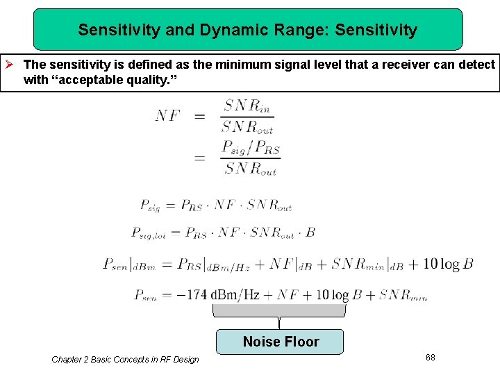
Sensitivity and Dynamic Range: Sensitivity Ø The sensitivity is defined as the minimum signal level that a receiver can detect with “acceptable quality. ” Noise Floor Chapter 2 Basic Concepts in RF Design 68
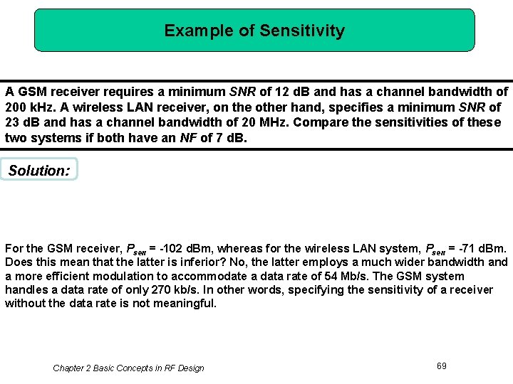
Example of Sensitivity A GSM receiver requires a minimum SNR of 12 d. B and has a channel bandwidth of 200 k. Hz. A wireless LAN receiver, on the other hand, specifies a minimum SNR of 23 d. B and has a channel bandwidth of 20 MHz. Compare the sensitivities of these two systems if both have an NF of 7 d. B. Solution: For the GSM receiver, Psen = -102 d. Bm, whereas for the wireless LAN system, Psen = -71 d. Bm. Does this mean that the latter is inferior? No, the latter employs a much wider bandwidth and a more efficient modulation to accommodate a data rate of 54 Mb/s. The GSM system handles a data rate of only 270 kb/s. In other words, specifying the sensitivity of a receiver without the data rate is not meaningful. Chapter 2 Basic Concepts in RF Design 69
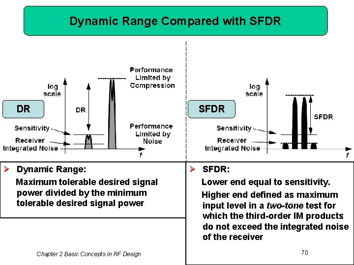
Dynamic Range Compared with SFDR DR Ø Dynamic Range: Maximum tolerable desired signal power divided by the minimum tolerable desired signal power Chapter 2 Basic Concepts in RF Design Ø SFDR: Lower end equal to sensitivity. Higher end defined as maximum input level in a two-tone test for which the third-order IM products do not exceed the integrated noise of the receiver 70
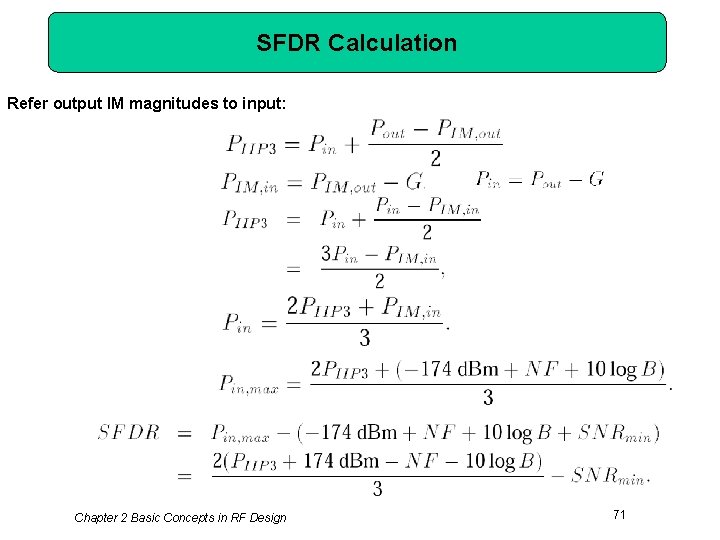
SFDR Calculation Refer output IM magnitudes to input: Chapter 2 Basic Concepts in RF Design 71
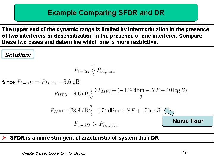
Example Comparing SFDR and DR The upper end of the dynamic range is limited by intermodulation in the presence of two interferers or desensitization in the presence of one interferer. Compare these two cases and determine which one is more restrictive. Solution: Since Noise floor Ø SFDR is a more stringent characteristic of system than DR Chapter 2 Basic Concepts in RF Design 72
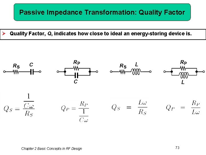
Passive Impedance Transformation: Quality Factor Ø Quality Factor, Q, indicates how close to ideal an energy-storing device is. Chapter 2 Basic Concepts in RF Design 73
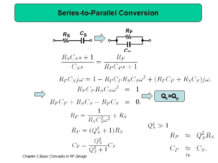
Series-to-Parallel Conversion Qs=Qp Chapter 2 Basic Concepts in RF Design 74
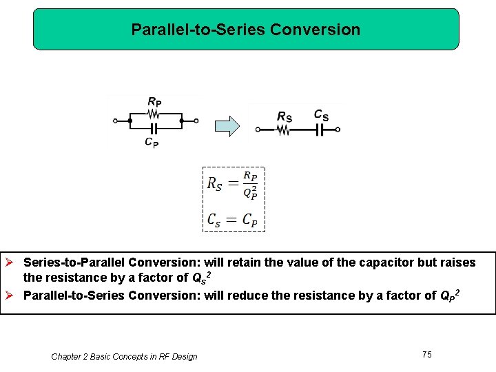
Parallel-to-Series Conversion Ø Series-to-Parallel Conversion: will retain the value of the capacitor but raises the resistance by a factor of Qs 2 Ø Parallel-to-Series Conversion: will reduce the resistance by a factor of QP 2 Chapter 2 Basic Concepts in RF Design 75
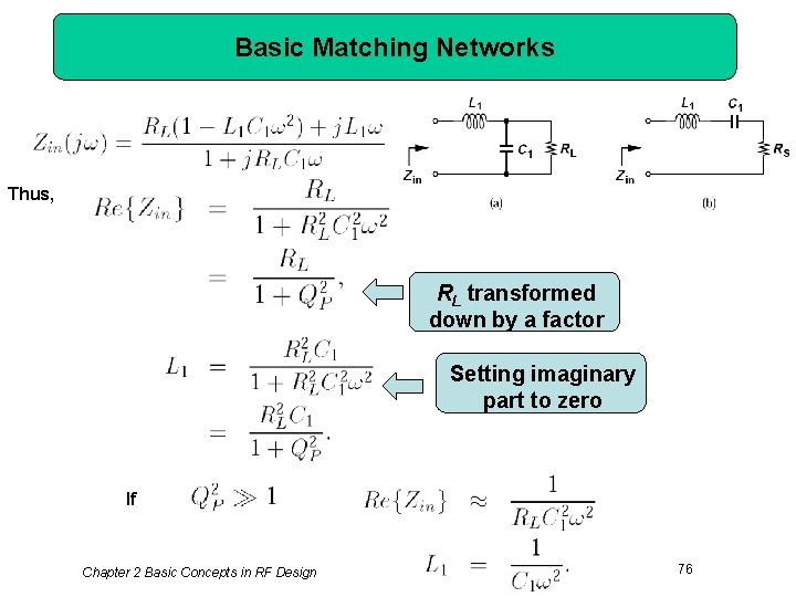
Basic Matching Networks Thus, RL transformed down by a factor Setting imaginary part to zero If Chapter 2 Basic Concepts in RF Design 76
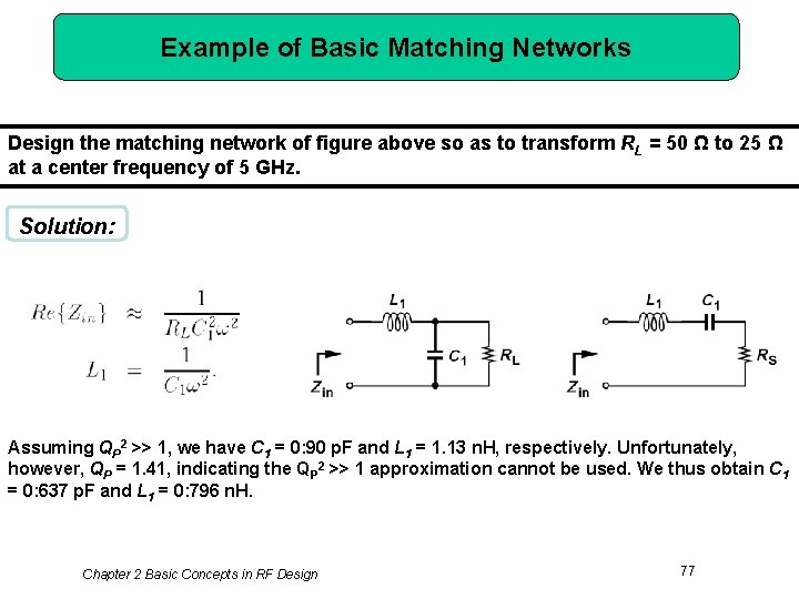
Example of Basic Matching Networks Design the matching network of figure above so as to transform RL = 50 Ω to 25 Ω at a center frequency of 5 GHz. Solution: Assuming QP 2 >> 1, we have C 1 = 0: 90 p. F and L 1 = 1. 13 n. H, respectively. Unfortunately, however, QP = 1. 41, indicating the QP 2 >> 1 approximation cannot be used. We thus obtain C 1 = 0: 637 p. F and L 1 = 0: 796 n. H. Chapter 2 Basic Concepts in RF Design 77
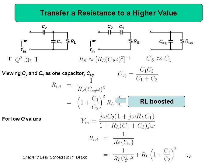
Transfer a Resistance to a Higher Value If Viewing C 2 and C 1 as one capacitor, Ceq RL boosted For low Q values Chapter 2 Basic Concepts in RF Design 78
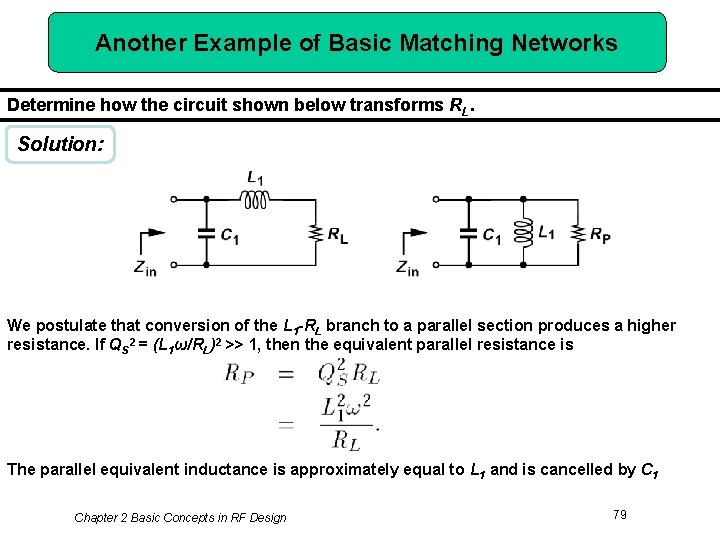
Another Example of Basic Matching Networks Determine how the circuit shown below transforms RL. Solution: We postulate that conversion of the L 1 -RL branch to a parallel section produces a higher resistance. If QS 2 = (L 1ω/RL)2 >> 1, then the equivalent parallel resistance is The parallel equivalent inductance is approximately equal to L 1 and is cancelled by C 1 Chapter 2 Basic Concepts in RF Design 79
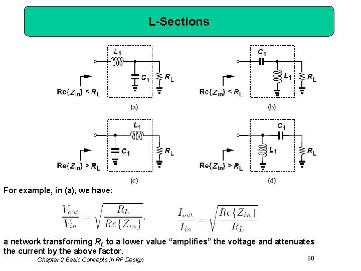
L-Sections For example, in (a), we have: a network transforming RL to a lower value “amplifies” the voltage and attenuates the current by the above factor. Chapter 2 Basic Concepts in RF Design 80
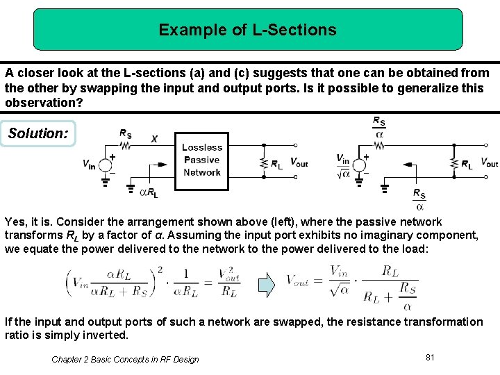
Example of L-Sections A closer look at the L-sections (a) and (c) suggests that one can be obtained from the other by swapping the input and output ports. Is it possible to generalize this observation? Solution: Yes, it is. Consider the arrangement shown above (left), where the passive network transforms RL by a factor of α. Assuming the input port exhibits no imaginary component, we equate the power delivered to the network to the power delivered to the load: If the input and output ports of such a network are swapped, the resistance transformation ratio is simply inverted. Chapter 2 Basic Concepts in RF Design 81
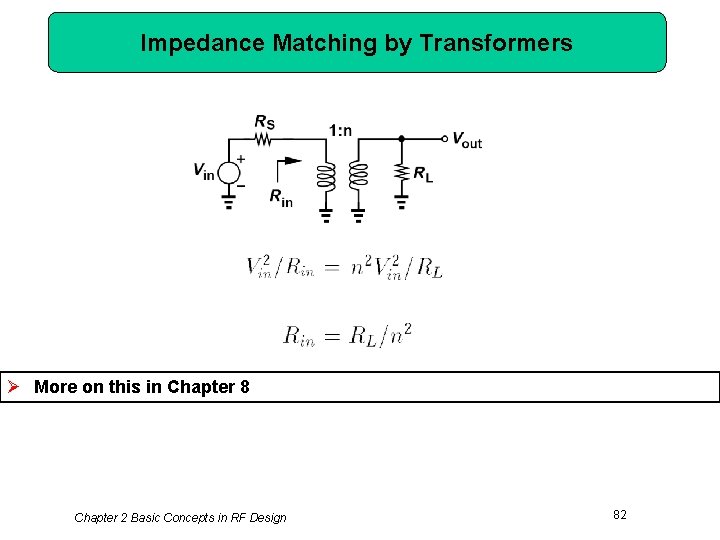
Impedance Matching by Transformers Ø More on this in Chapter 8 Chapter 2 Basic Concepts in RF Design 82
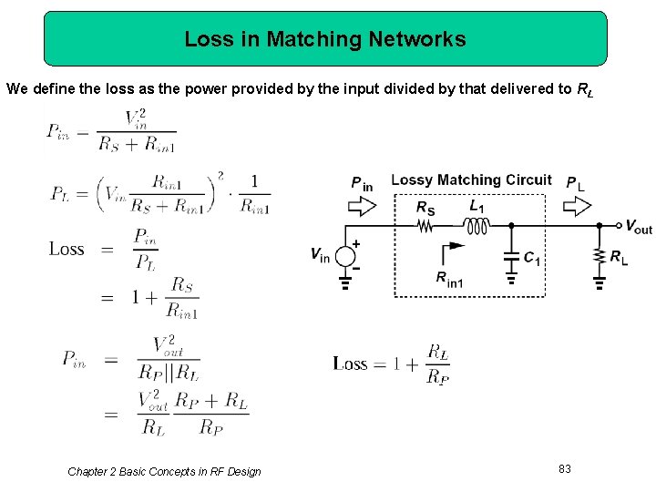
Loss in Matching Networks We define the loss as the power provided by the input divided by that delivered to RL Chapter 2 Basic Concepts in RF Design 83
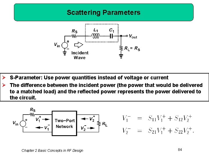
Scattering Parameters Ø S-Parameter: Use power quantities instead of voltage or current Ø The difference between the incident power (the power that would be delivered to a matched load) and the reflected power represents the power delivered to the circuit. Chapter 2 Basic Concepts in RF Design 84
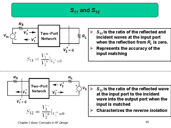
S 11 and S 12 Ø S 11 is the ratio of the reflected and incident waves at the input port when the reflection from RL is zero. Ø Represents the accuracy of the input matching Ø S 12 is the ratio of the reflected wave at the input port to the incident wave into the output port when the input is matched Ø Characterizes the reverse isolation Chapter 2 Basic Concepts in RF Design 85
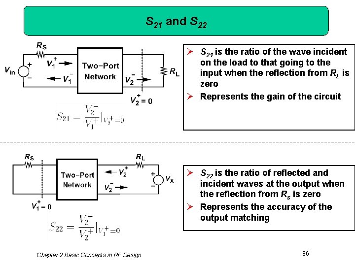
S 21 and S 22 Ø S 21 is the ratio of the wave incident on the load to that going to the input when the reflection from RL is zero Ø Represents the gain of the circuit Ø S 22 is the ratio of reflected and incident waves at the output when the reflection from Rs is zero Ø Represents the accuracy of the output matching Chapter 2 Basic Concepts in RF Design 86
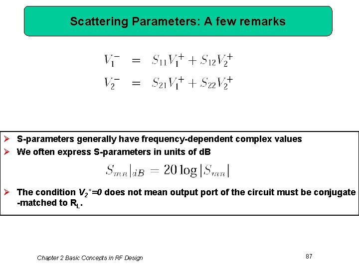
Scattering Parameters: A few remarks Ø S-parameters generally have frequency-dependent complex values Ø We often express S-parameters in units of d. B Ø The condition V 2+=0 does not mean output port of the circuit must be conjugate -matched to RL. Chapter 2 Basic Concepts in RF Design 87
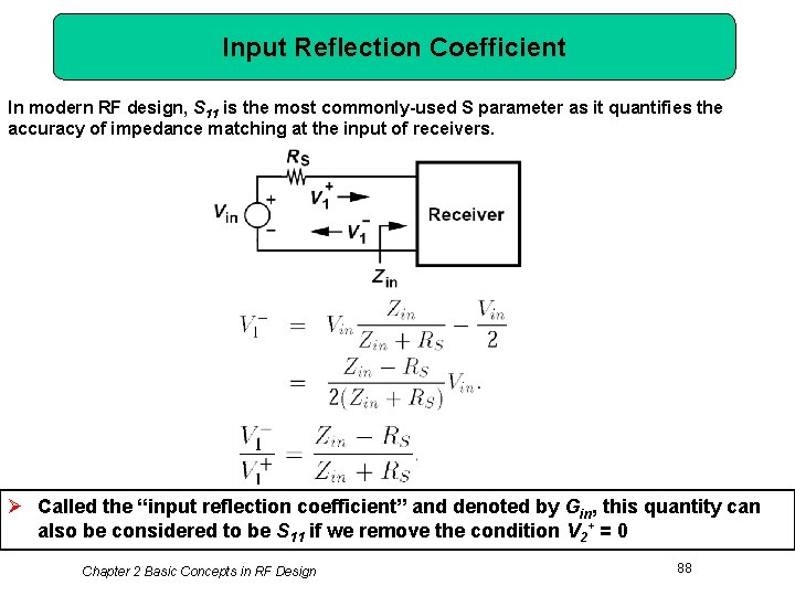
Input Reflection Coefficient In modern RF design, S 11 is the most commonly-used S parameter as it quantifies the accuracy of impedance matching at the input of receivers. Ø Called the “input reflection coefficient” and denoted by Gin, this quantity can also be considered to be S 11 if we remove the condition V 2+ = 0 Chapter 2 Basic Concepts in RF Design 88
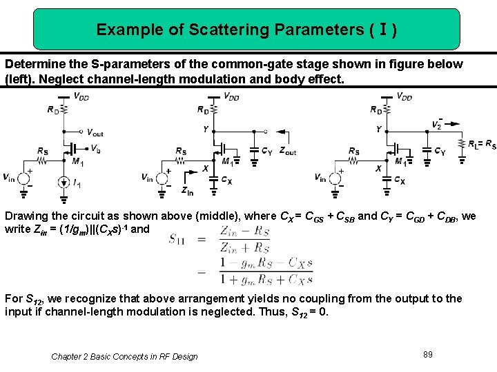
Example of Scattering Parameters (Ⅰ) Determine the S-parameters of the common-gate stage shown in figure below (left). Neglect channel-length modulation and body effect. Drawing the circuit as shown above (middle), where CX = CGS + CSB and CY = CGD + CDB, we write Zin = (1/gm)||(CXs)-1 and For S 12, we recognize that above arrangement yields no coupling from the output to the input if channel-length modulation is neglected. Thus, S 12 = 0. Chapter 2 Basic Concepts in RF Design 89
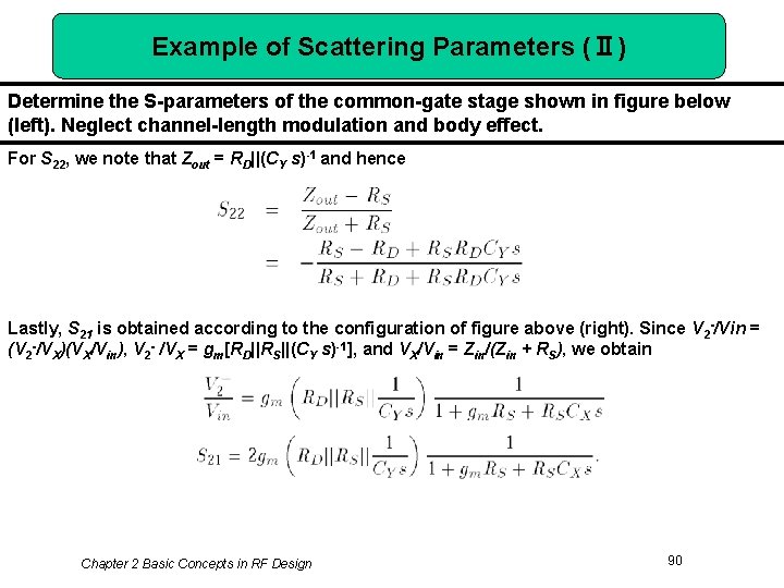
Example of Scattering Parameters (Ⅱ) Determine the S-parameters of the common-gate stage shown in figure below (left). Neglect channel-length modulation and body effect. For S 22, we note that Zout = RD||(CY s)-1 and hence Lastly, S 21 is obtained according to the configuration of figure above (right). Since V 2 -/Vin = (V 2 -/VX)(VX/Vin), V 2 - /VX = gm[RD||RS||(CY s)-1], and VX/Vin = Zin/(Zin + RS), we obtain Chapter 2 Basic Concepts in RF Design 90
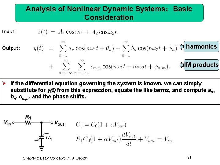
Analysis of Nonlinear Dynamic Systems:Basic Consideration Input: harmonics Output: IM products Ø If the differential equation governing the system is known, we can simply substitute for y(t) from this expression, equate the like terms, and compute an, bn, cm, n, and the phase shifts. Chapter 2 Basic Concepts in RF Design 91
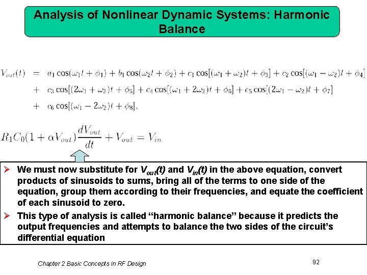
Analysis of Nonlinear Dynamic Systems: Harmonic Balance Ø We must now substitute for Vout(t) and Vin(t) in the above equation, convert products of sinusoids to sums, bring all of the terms to one side of the equation, group them according to their frequencies, and equate the coefficient of each sinusoid to zero. Ø This type of analysis is called “harmonic balance” because it predicts the output frequencies and attempts to balance the two sides of the circuit’s differential equation Chapter 2 Basic Concepts in RF Design 92
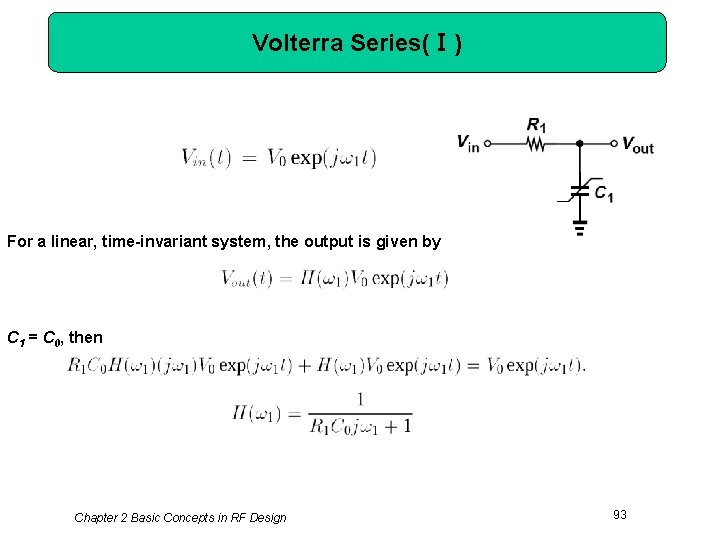
Volterra Series(Ⅰ) For a linear, time-invariant system, the output is given by C 1 = C 0, then Chapter 2 Basic Concepts in RF Design 93
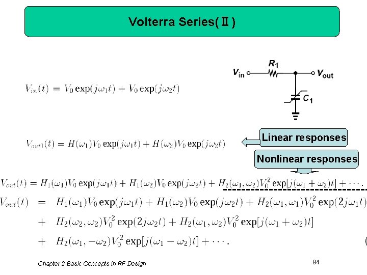
Volterra Series(Ⅱ) Linear responses Nonlinear responses Chapter 2 Basic Concepts in RF Design 94
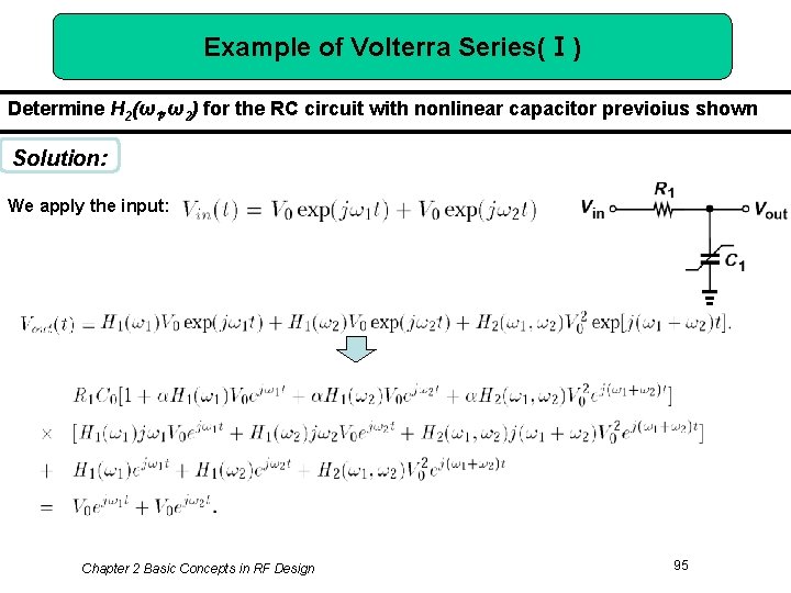
Example of Volterra Series(Ⅰ) Determine H 2(ω1, ω2) for the RC circuit with nonlinear capacitor previoius shown Solution: We apply the input: Chapter 2 Basic Concepts in RF Design 95
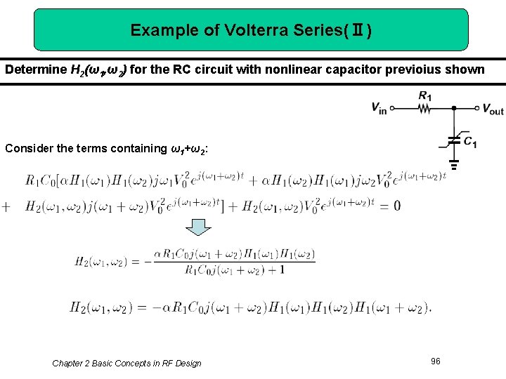
Example of Volterra Series(Ⅱ) Determine H 2(ω1, ω2) for the RC circuit with nonlinear capacitor previoius shown Consider the terms containing ω1+ω2: Chapter 2 Basic Concepts in RF Design 96
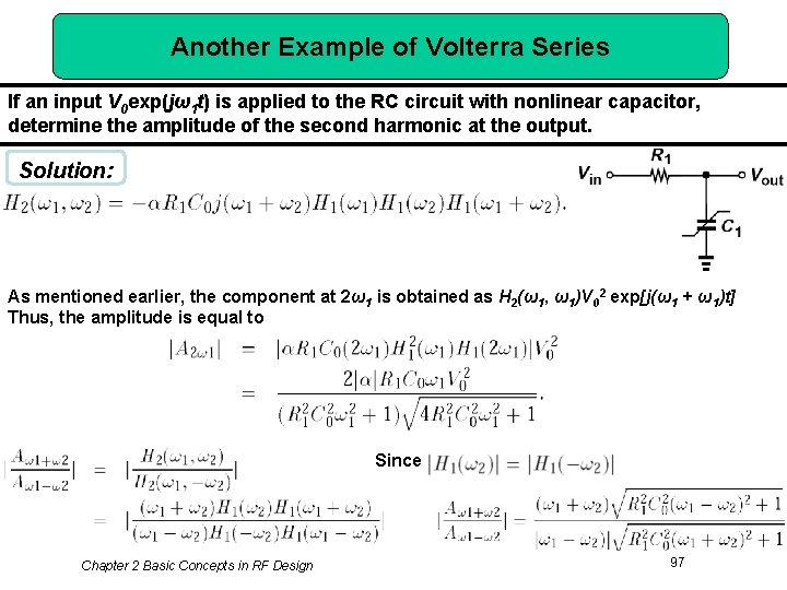
Another Example of Volterra Series If an input V 0 exp(jω1 t) is applied to the RC circuit with nonlinear capacitor, determine the amplitude of the second harmonic at the output. Solution: As mentioned earlier, the component at 2ω1 is obtained as H 2(ω1, ω1)V 02 exp[j(ω1 + ω1)t] Thus, the amplitude is equal to Since Chapter 2 Basic Concepts in RF Design 97
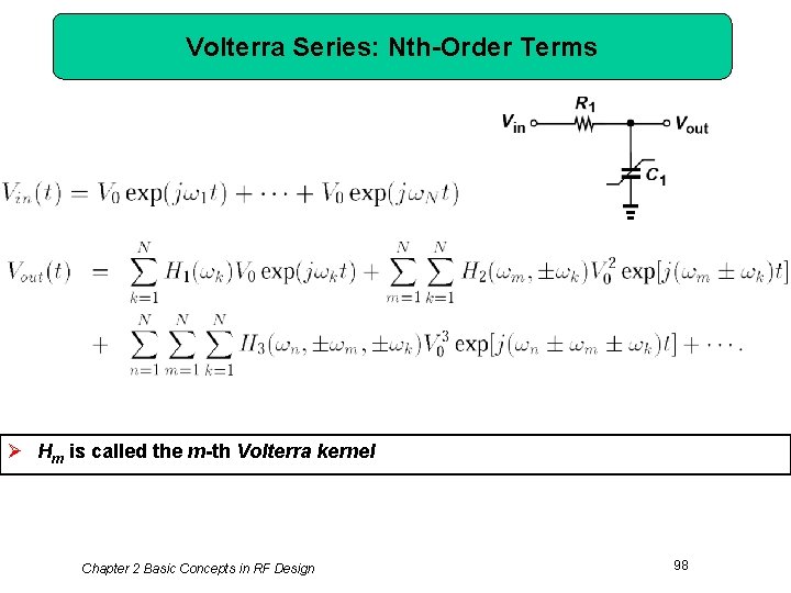
Volterra Series: Nth-Order Terms Ø Hm is called the m-th Volterra kernel Chapter 2 Basic Concepts in RF Design 98
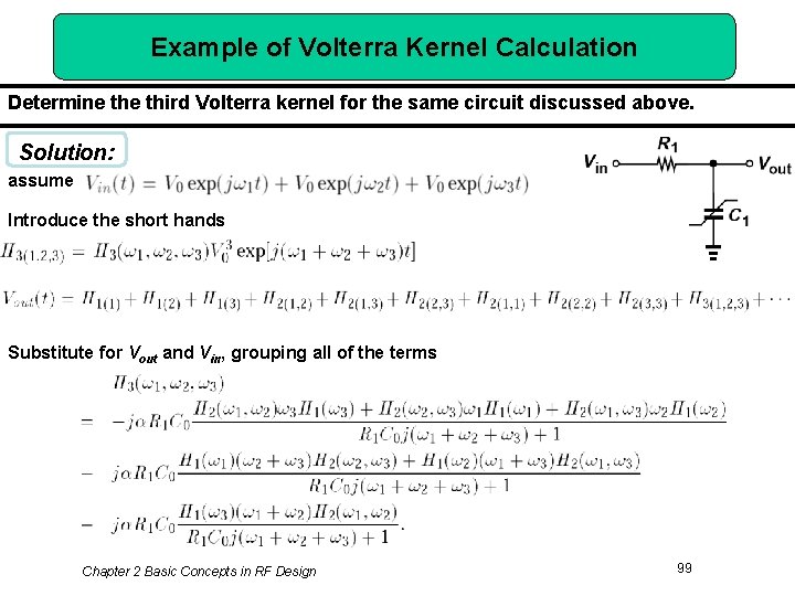
Example of Volterra Kernel Calculation Determine third Volterra kernel for the same circuit discussed above. Solution: assume Introduce the short hands Substitute for Vout and Vin, grouping all of the terms Chapter 2 Basic Concepts in RF Design 99
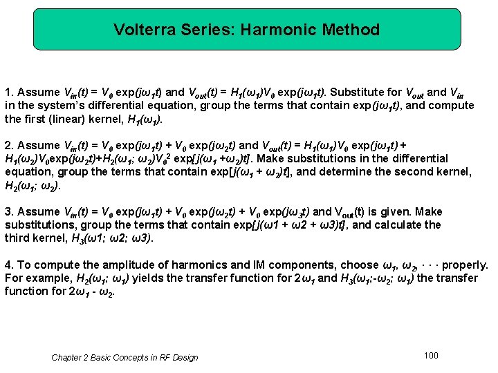
Volterra Series: Harmonic Method 1. Assume Vin(t) = V 0 exp(jω1 t) and Vout(t) = H 1(ω1)V 0 exp(jω1 t). Substitute for Vout and Vin in the system’s differential equation, group the terms that contain exp(jω1 t), and compute the first (linear) kernel, H 1(ω1). 2. Assume Vin(t) = V 0 exp(jω1 t) + V 0 exp(jω2 t) and Vout(t) = H 1(ω1)V 0 exp(jω1 t) + H 1(ω2)V 0 exp(jω2 t)+H 2(ω1; ω2)V 02 exp[j(ω1 +ω2)t]. Make substitutions in the differential equation, group the terms that contain exp[j(ω1 + ω2)t], and determine the second kernel, H 2(ω1; ω2). 3. Assume Vin(t) = V 0 exp(jω1 t) + V 0 exp(jω2 t) + V 0 exp(jω3 t) and Vout(t) is given. Make substitutions, group the terms that contain exp[j(ω1 + ω2 + ω3)t], and calculate third kernel, H 3(ω1; ω2; ω3). 4. To compute the amplitude of harmonics and IM components, choose ω1, ω2, · · · properly. For example, H 2(ω1; ω1) yields the transfer function for 2ω1 and H 3(ω1; -ω2; ω1) the transfer function for 2ω1 - ω2. Chapter 2 Basic Concepts in RF Design 100
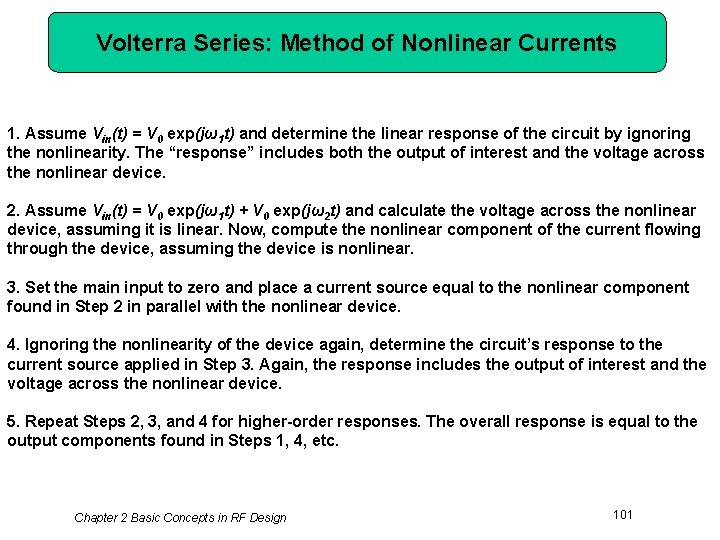
Volterra Series: Method of Nonlinear Currents 1. Assume Vin(t) = V 0 exp(jω1 t) and determine the linear response of the circuit by ignoring the nonlinearity. The “response” includes both the output of interest and the voltage across the nonlinear device. 2. Assume Vin(t) = V 0 exp(jω1 t) + V 0 exp(jω2 t) and calculate the voltage across the nonlinear device, assuming it is linear. Now, compute the nonlinear component of the current flowing through the device, assuming the device is nonlinear. 3. Set the main input to zero and place a current source equal to the nonlinear component found in Step 2 in parallel with the nonlinear device. 4. Ignoring the nonlinearity of the device again, determine the circuit’s response to the current source applied in Step 3. Again, the response includes the output of interest and the voltage across the nonlinear device. 5. Repeat Steps 2, 3, and 4 for higher-order responses. The overall response is equal to the output components found in Steps 1, 4, etc. Chapter 2 Basic Concepts in RF Design 101

Example Using Method of Nonlinear Currents (Ⅰ) Determine H 3(ω1, ω2, ω3) for the circuit below. Solution: Step 1 The voltage across the capacitor is equal to: Step 2 Compute the nonlinear current flowing through C 1 Chapter 2 Basic Concepts in RF Design 102
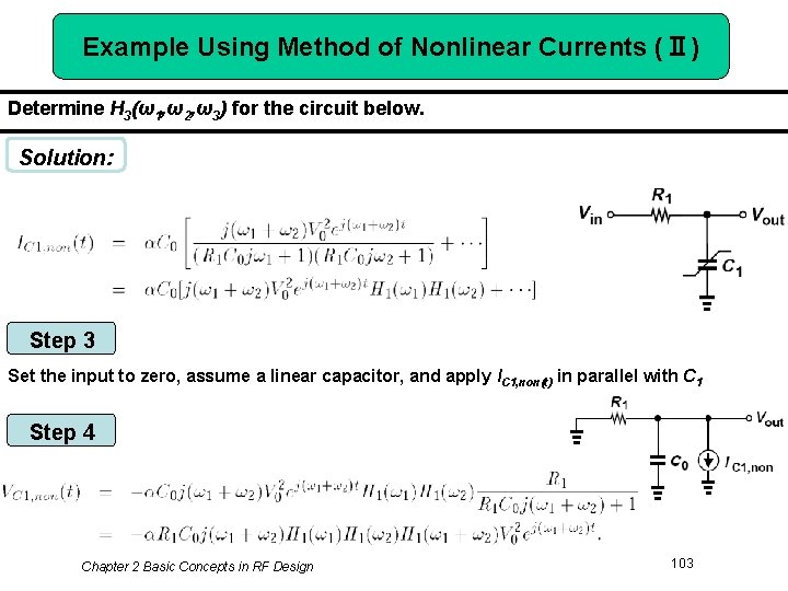
Example Using Method of Nonlinear Currents (Ⅱ) Determine H 3(ω1, ω2, ω3) for the circuit below. Solution: Step 3 Set the input to zero, assume a linear capacitor, and apply IC 1, non(t) in parallel with C 1 Step 4 Chapter 2 Basic Concepts in RF Design 103
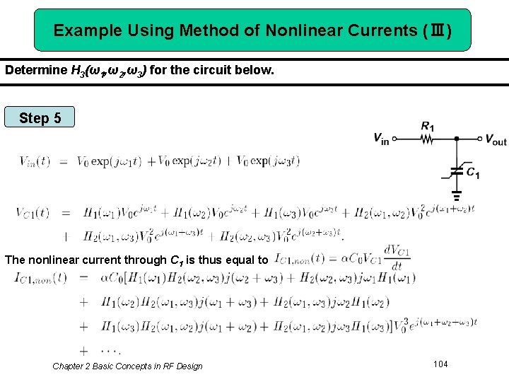
Example Using Method of Nonlinear Currents (Ⅲ) Determine H 3(ω1, ω2, ω3) for the circuit below. Step 5 The nonlinear current through C 1 is thus equal to Chapter 2 Basic Concepts in RF Design 104
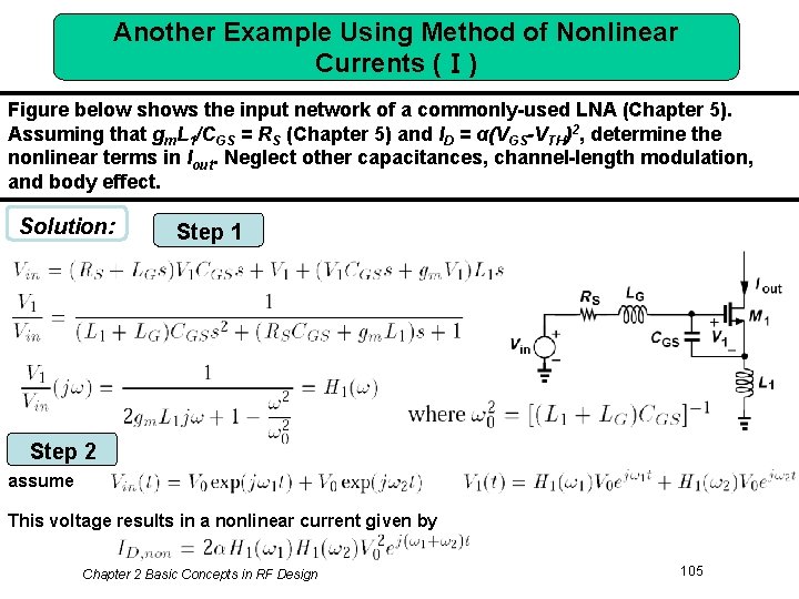
Another Example Using Method of Nonlinear Currents (Ⅰ) Figure below shows the input network of a commonly-used LNA (Chapter 5). Assuming that gm. L 1/CGS = RS (Chapter 5) and ID = α(VGS-VTH)2, determine the nonlinear terms in Iout. Neglect other capacitances, channel-length modulation, and body effect. Solution: Step 1 Step 2 assume This voltage results in a nonlinear current given by Chapter 2 Basic Concepts in RF Design 105
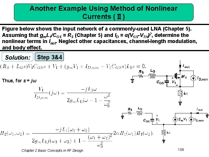
Another Example Using Method of Nonlinear Currents (Ⅱ) Figure below shows the input network of a commonly-used LNA (Chapter 5). Assuming that gm. L 1/CGS = RS (Chapter 5) and ID = α(VGS-VTH)2, determine the nonlinear terms in Iout. Neglect other capacitances, channel-length modulation, and body effect. Solution: Step 3&4 Thus, for s = jω Chapter 2 Basic Concepts in RF Design 106
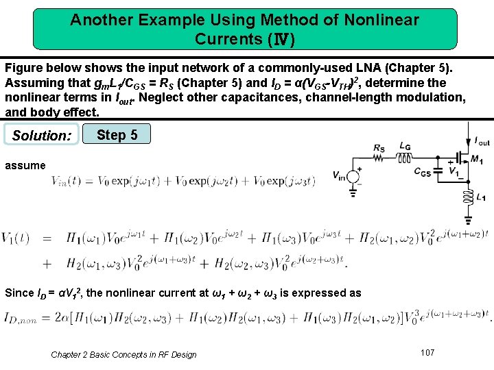
Another Example Using Method of Nonlinear Currents (Ⅳ) Figure below shows the input network of a commonly-used LNA (Chapter 5). Assuming that gm. L 1/CGS = RS (Chapter 5) and ID = α(VGS-VTH)2, determine the nonlinear terms in Iout. Neglect other capacitances, channel-length modulation, and body effect. Solution: Step 5 assume Since ID = αV 12, the nonlinear current at ω1 + ω2 + ω3 is expressed as Chapter 2 Basic Concepts in RF Design 107
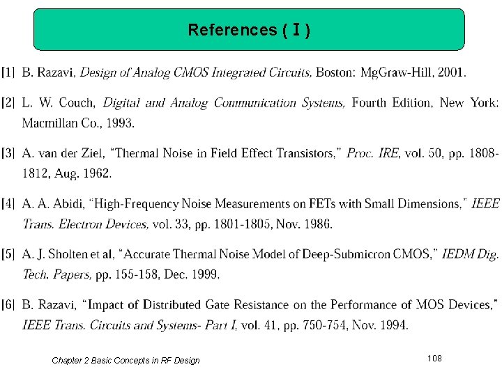
References (Ⅰ) Chapter 2 Basic Concepts in RF Design 108
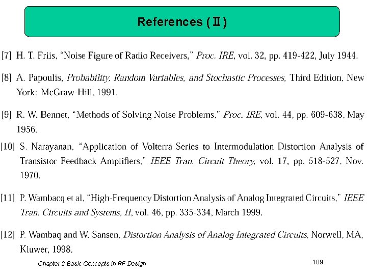
References (Ⅱ) Chapter 2 Basic Concepts in RF Design 109
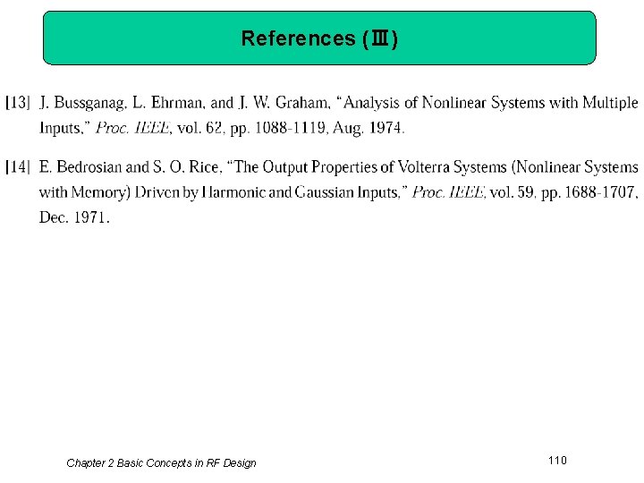
References (Ⅲ) Chapter 2 Basic Concepts in RF Design 110
- Slides: 110