
CHAPTER 18 TRANSISTORS AND THYRISTORS 1 BIPOLAR JUNCTION
CHAPTER 18 TRANSISTORS AND THYRISTORS 1
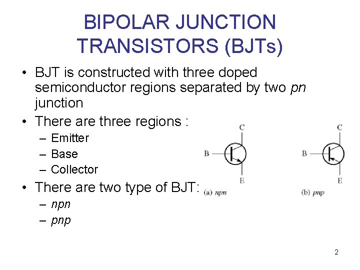
BIPOLAR JUNCTION TRANSISTORS (BJTs) • BJT is constructed with three doped semiconductor regions separated by two pn junction • There are three regions : – Emitter – Base – Collector • There are two type of BJT: – npn – pnp 2
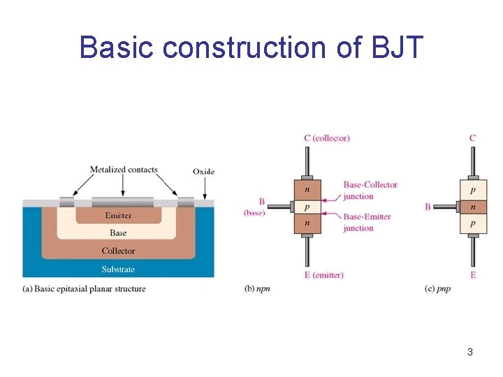
Basic construction of BJT 3
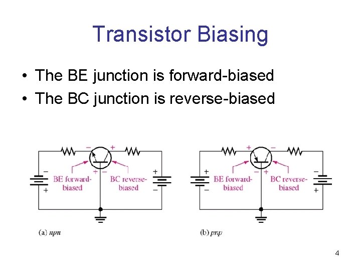
Transistor Biasing • The BE junction is forward-biased • The BC junction is reverse-biased 4
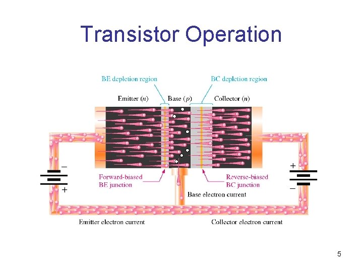
Transistor Operation 5
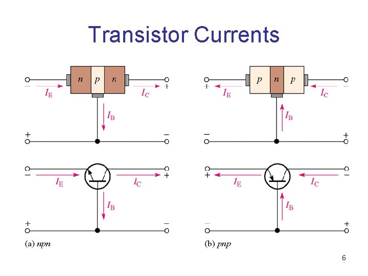
Transistor Currents 6
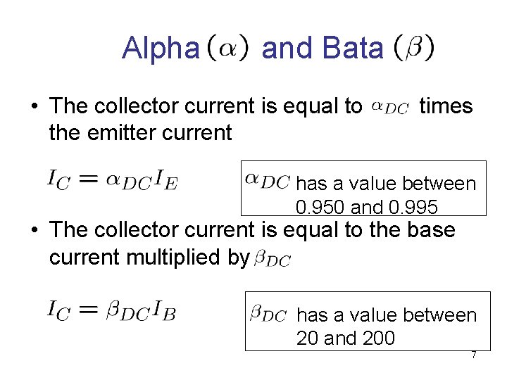
Alpha and Bata • The collector current is equal to the emitter current times has a value between 0. 950 and 0. 995 • The collector current is equal to the base current multiplied by has a value between 20 and 200 7
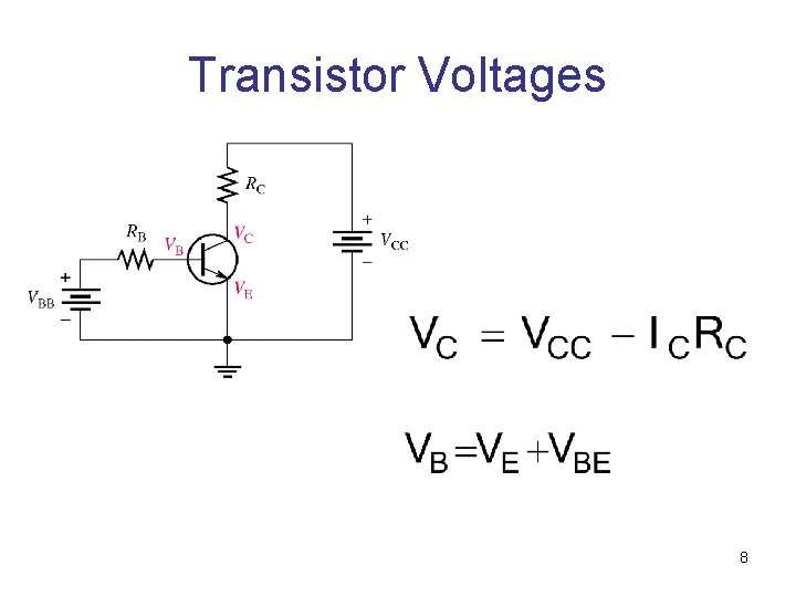
Transistor Voltages 8
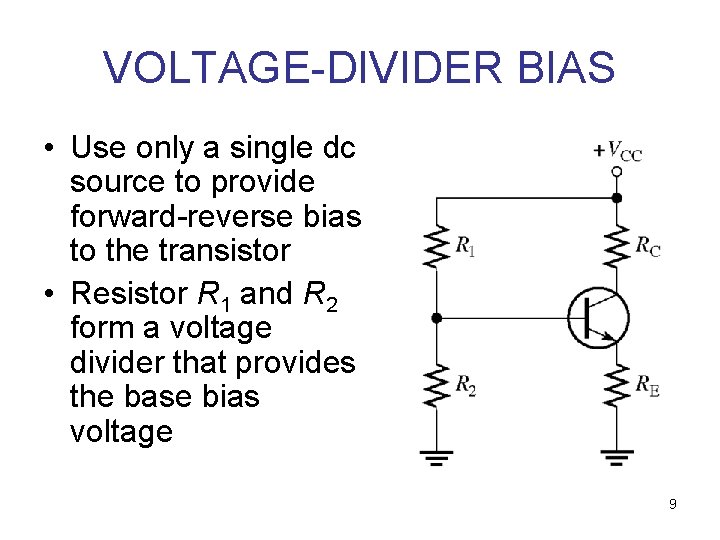
VOLTAGE-DIVIDER BIAS • Use only a single dc source to provide forward-reverse bias to the transistor • Resistor R 1 and R 2 form a voltage divider that provides the base bias voltage 9
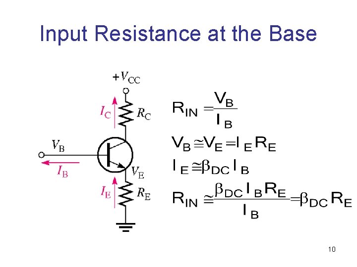
Input Resistance at the Base 10
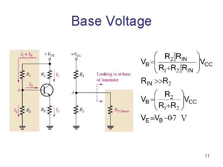
Base Voltage V 11
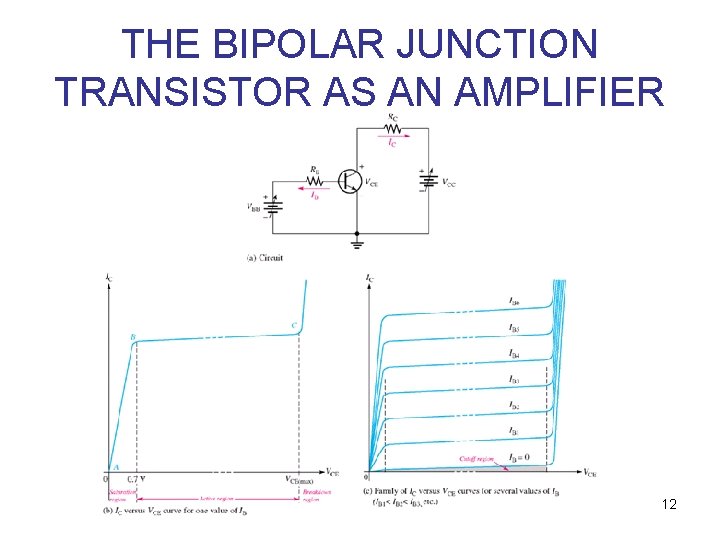
THE BIPOLAR JUNCTION TRANSISTOR AS AN AMPLIFIER 12
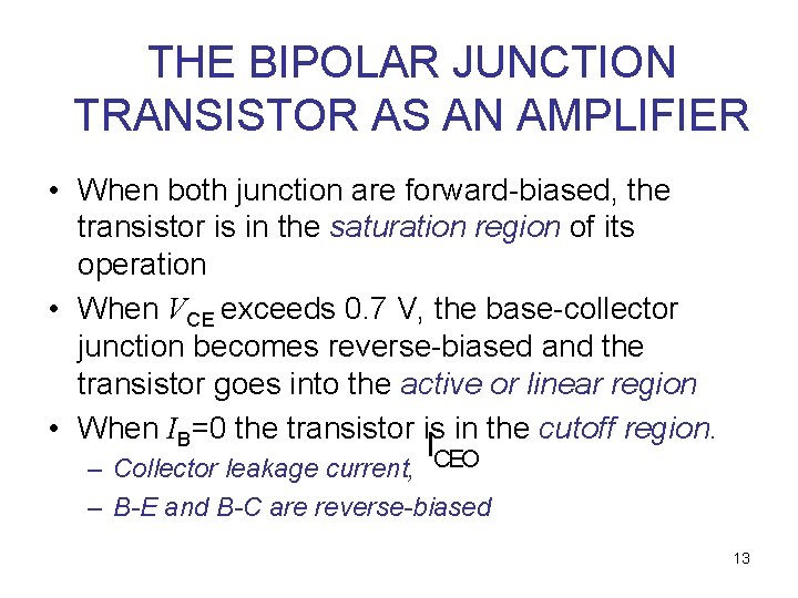
THE BIPOLAR JUNCTION TRANSISTOR AS AN AMPLIFIER • When both junction are forward-biased, the transistor is in the saturation region of its operation • When VCE exceeds 0. 7 V, the base-collector junction becomes reverse-biased and the transistor goes into the active or linear region • When IB=0 the transistor is in the cutoff region. ICEO – Collector leakage current, – B-E and B-C are reverse-biased 13

Load Line Operation 14
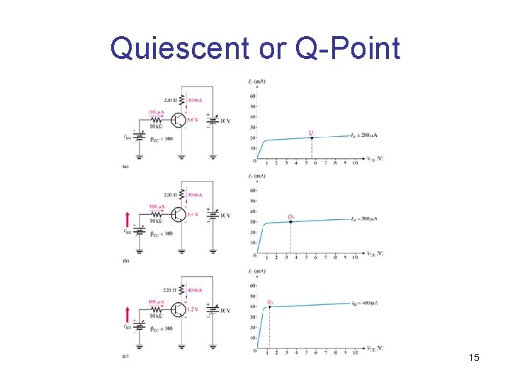
Quiescent or Q-Point 15
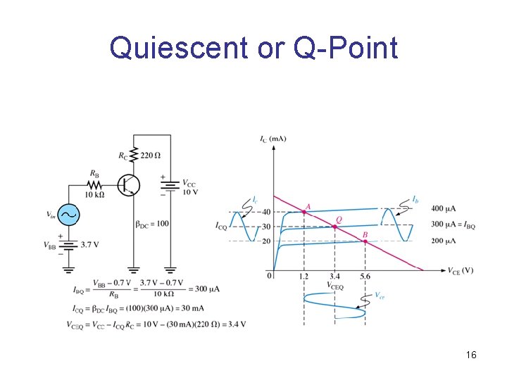
Quiescent or Q-Point 16
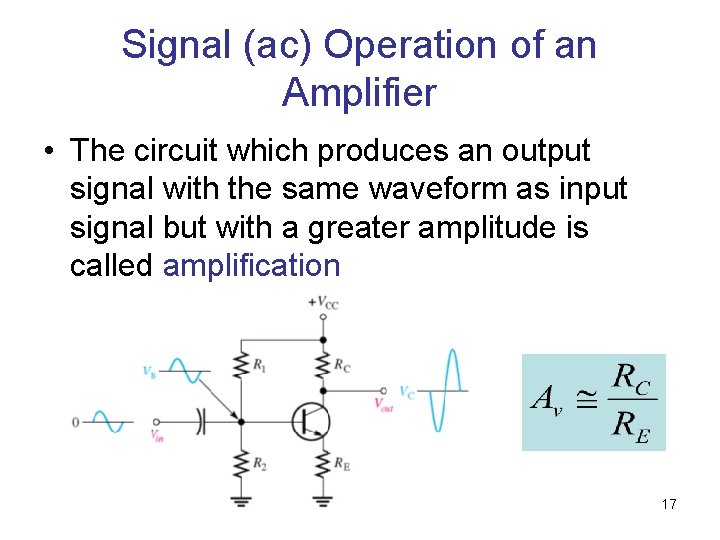
Signal (ac) Operation of an Amplifier • The circuit which produces an output signal with the same waveform as input signal but with a greater amplitude is called amplification 17
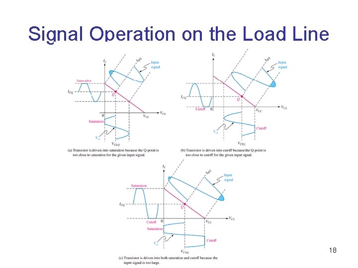
Signal Operation on the Load Line 18
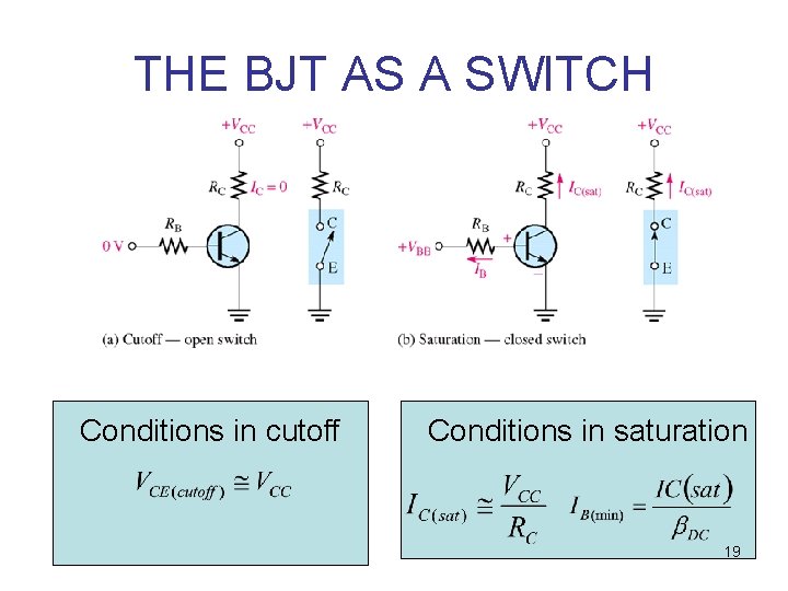
THE BJT AS A SWITCH Conditions in cutoff Conditions in saturation 19
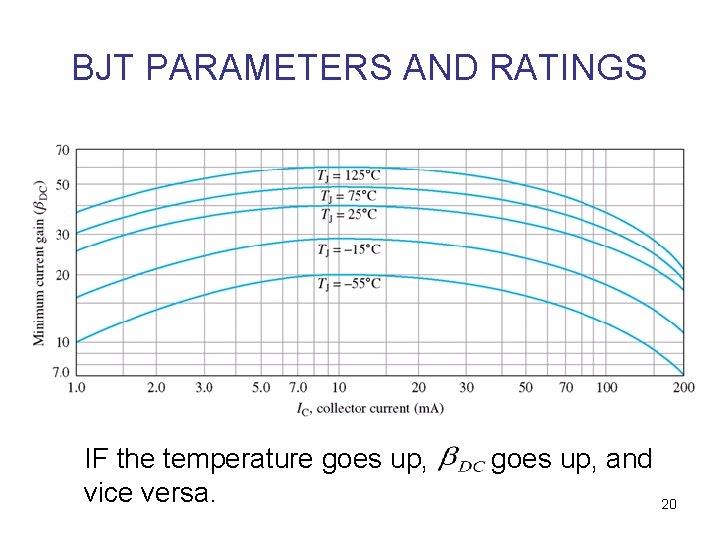
BJT PARAMETERS AND RATINGS IF the temperature goes up, vice versa. goes up, and 20
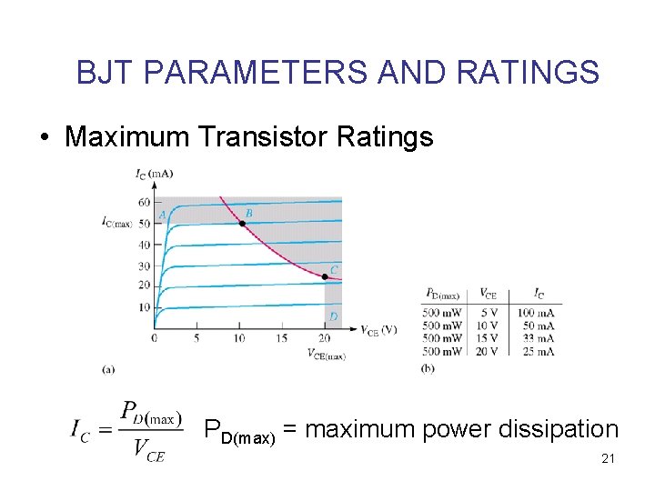
BJT PARAMETERS AND RATINGS • Maximum Transistor Ratings PD(max) = maximum power dissipation 21
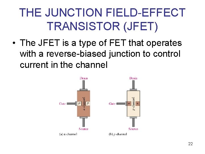
THE JUNCTION FIELD-EFFECT TRANSISTOR (JFET) • The JFET is a type of FET that operates with a reverse-biased junction to control current in the channel 22
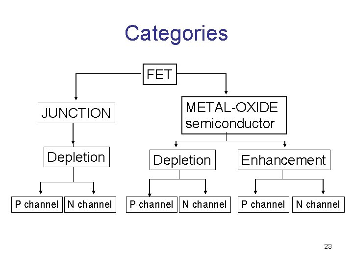
Categories FET JUNCTION Depletion P channel N channel METAL-OXIDE semiconductor Depletion P channel N channel Enhancement P channel N channel 23
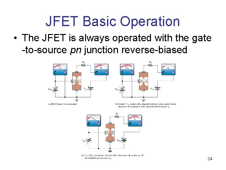
JFET Basic Operation • The JFET is always operated with the gate -to-source pn junction reverse-biased 24
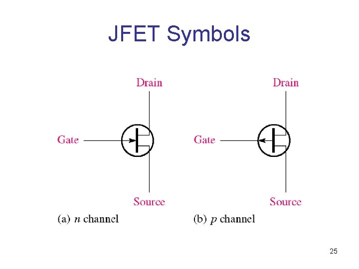
JFET Symbols 25

JFET CHARACTERISTICS IDSS (Drain to Source current with gate shorted) is maximum drain current occurring for VGS =0 V, and the value of VDS which ID becomes constant is the pinch-off voltage 26
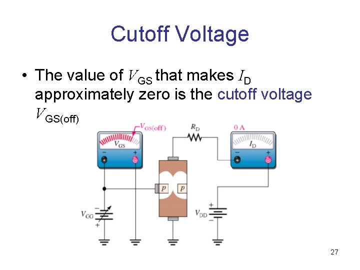
Cutoff Voltage • The value of VGS that makes ID approximately zero is the cutoff voltage VGS(off) 27
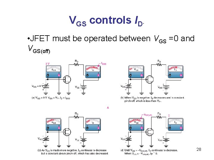
VGS controls ID. • JFET must be operated between VGS =0 and VGS(off) 28
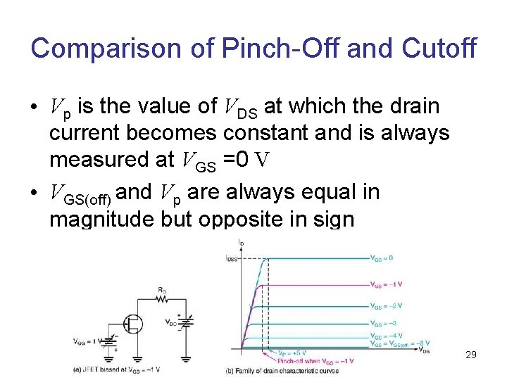
Comparison of Pinch-Off and Cutoff • Vp is the value of VDS at which the drain current becomes constant and is always measured at VGS =0 V • VGS(off) and Vp are always equal in magnitude but opposite in sign 29
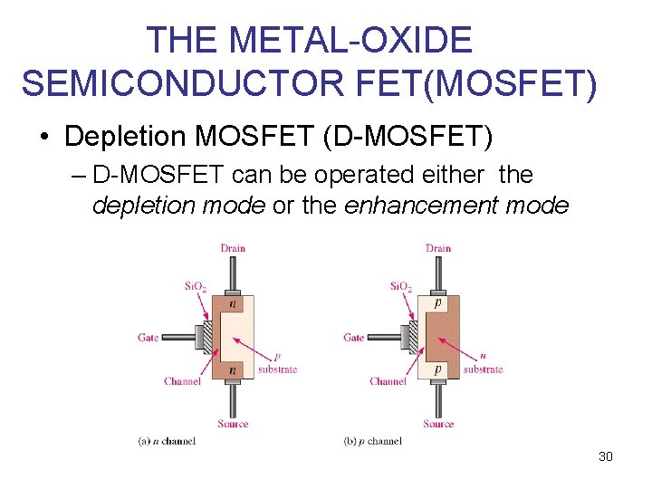
THE METAL-OXIDE SEMICONDUCTOR FET(MOSFET) • Depletion MOSFET (D-MOSFET) – D-MOSFET can be operated either the depletion mode or the enhancement mode 30
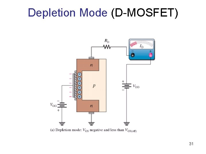
Depletion Mode (D-MOSFET) 31
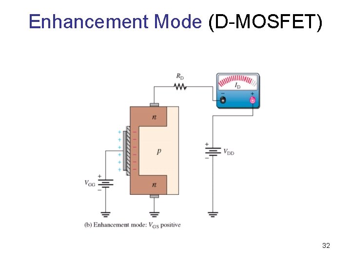
Enhancement Mode (D-MOSFET) 32
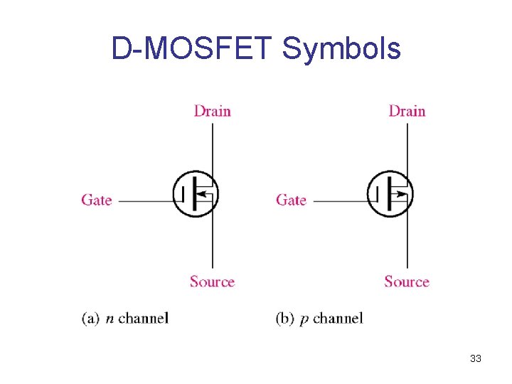
D-MOSFET Symbols 33
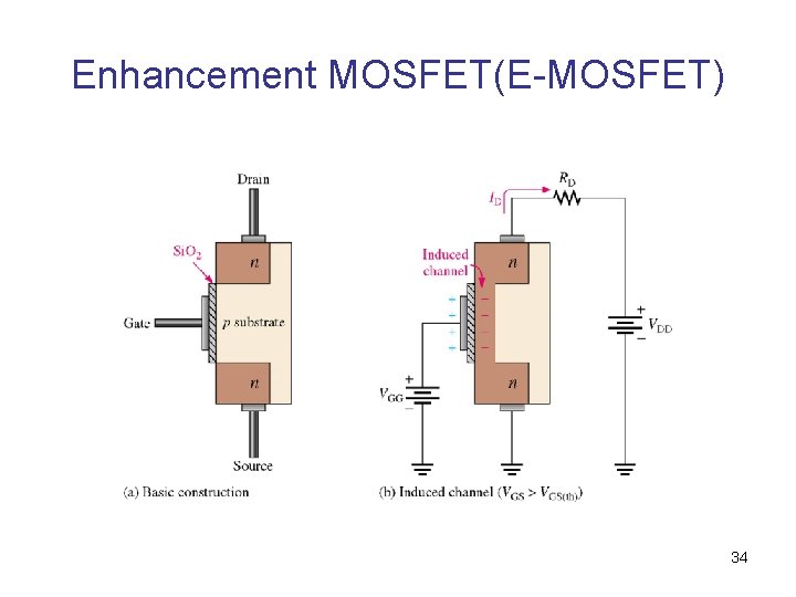
Enhancement MOSFET(E-MOSFET) 34
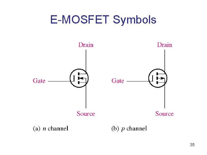
E-MOSFET Symbols 35
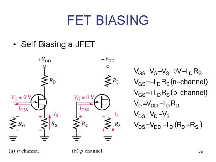
FET BIASING • Self-Biasing a JFET 36
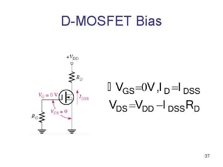
D-MOSFET Bias 37
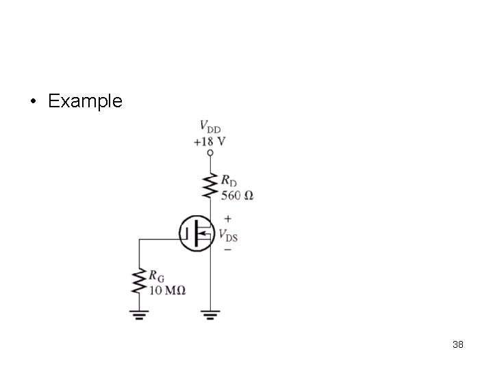
• Example 38
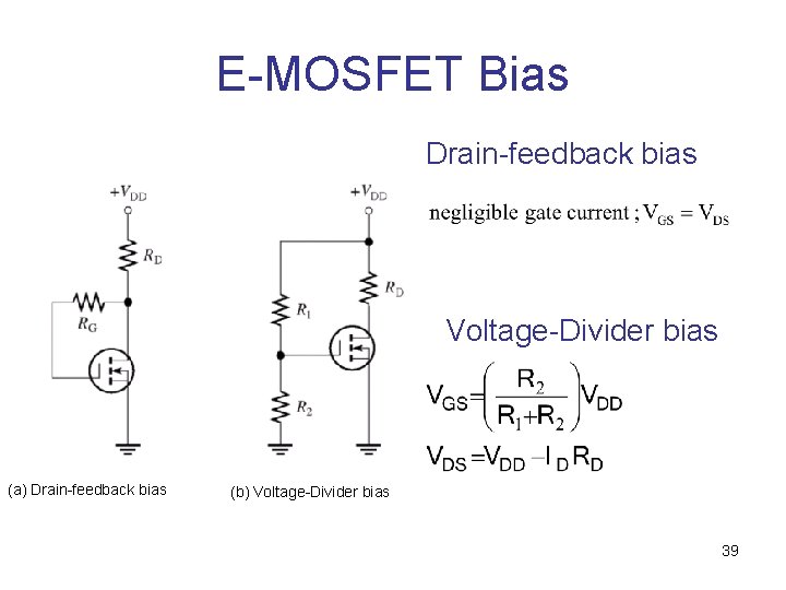
E-MOSFET Bias Drain-feedback bias Voltage-Divider bias (a) Drain-feedback bias (b) Voltage-Divider bias 39
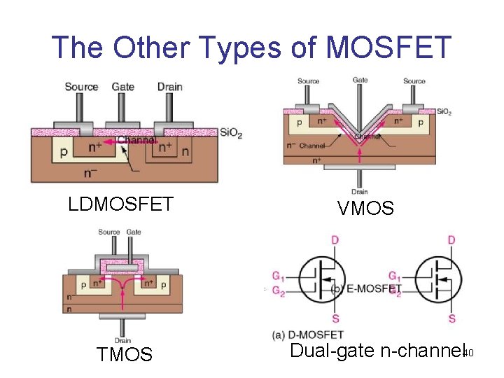
The Other Types of MOSFET LDMOSFET TMOS VMOS Dual-gate n-channel 40
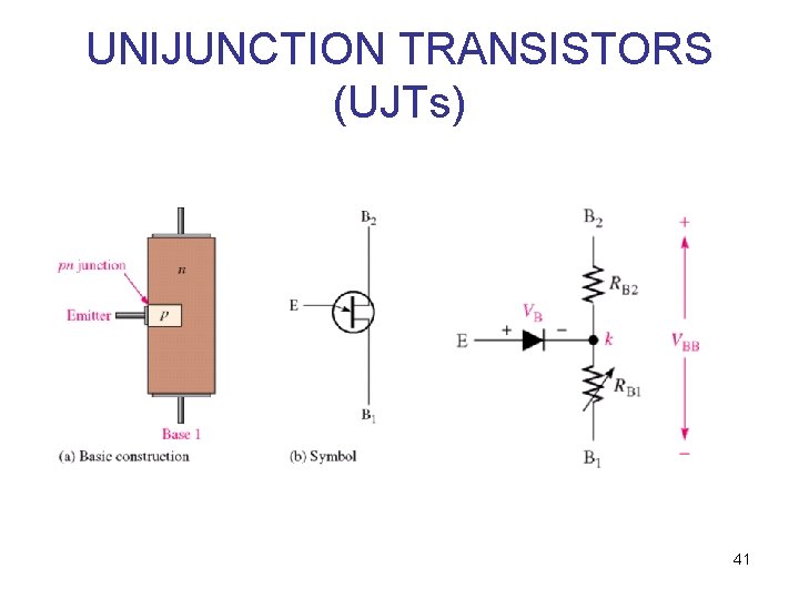
UNIJUNCTION TRANSISTORS (UJTs) 41
UJT operation • In normal UJT operation, base 2 (B 2) and the emitter are biased positive with respect to base 1 (B 1), and total resistance between B 1 and B 2 is RBB • The ratio RB 1/RBB is designated η and is defined as the intrinsic standoff ratio • It take an emitter voltage of VB + η *VBB to turn the UJT on, called the peak voltage • When the emitter voltage decreases, it reaches a value called the valley voltage, and the UJT turns off 42
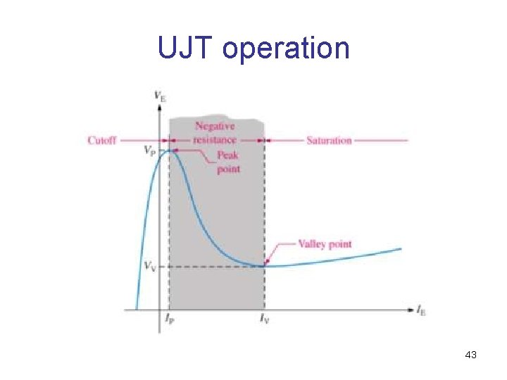
UJT operation 43
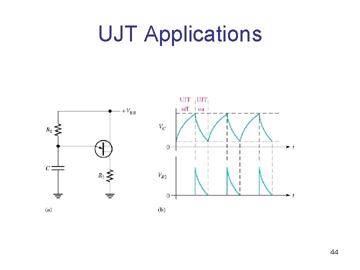
UJT Applications 44
THYRISTORS • Thyristors are devices constructed of four layers of semiconductive material such as the silicon-controlled rectifier (SCR), the diac, and the triac • When turned on (triggered), they become low-resistance current paths and remain, although the trigger is removed, until the current is reduced to a certain level or until they are turned off 45
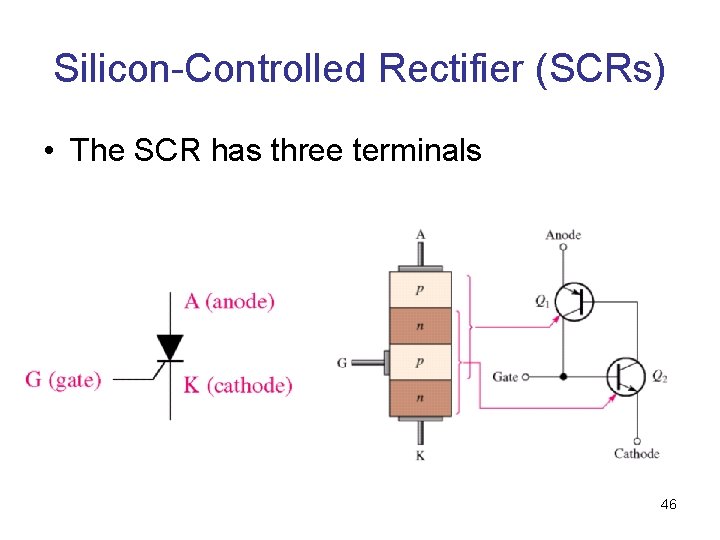
Silicon-Controlled Rectifier (SCRs) • The SCR has three terminals 46
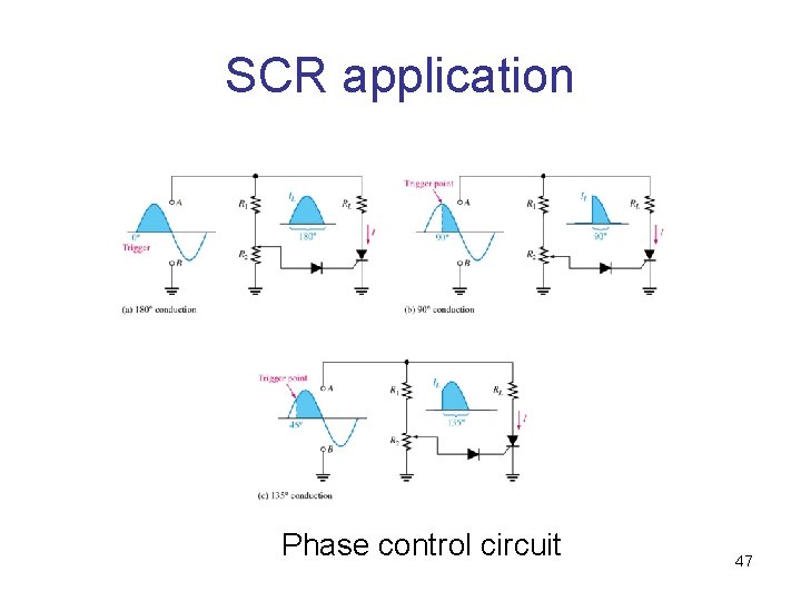
SCR application Phase control circuit 47
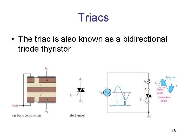
Triacs • The triac is also known as a bidirectional triode thyristor 48
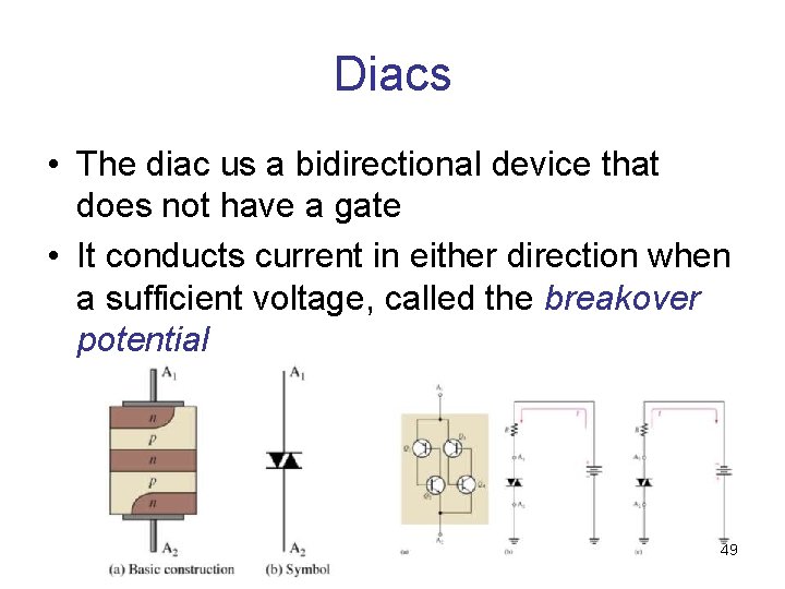
Diacs • The diac us a bidirectional device that does not have a gate • It conducts current in either direction when a sufficient voltage, called the breakover potential 49
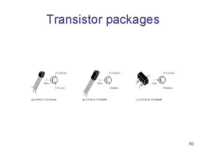
Transistor packages 50
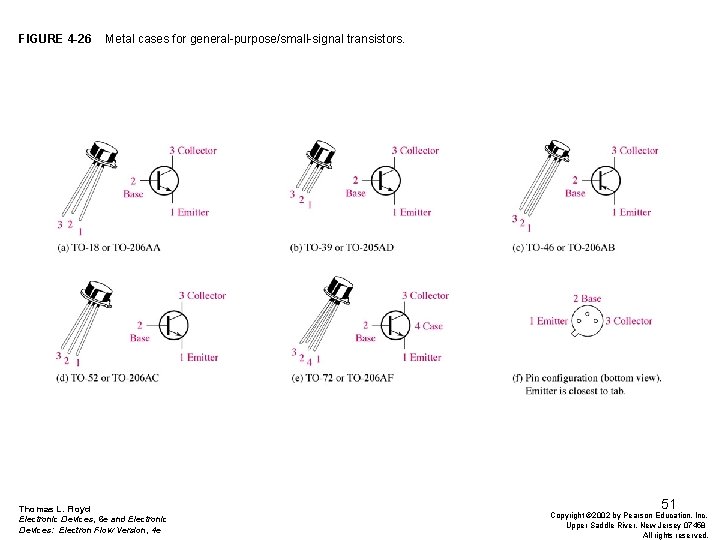
FIGURE 4 -26 Metal cases for general-purpose/small-signal transistors. Thomas L. Floyd Electronic Devices, 6 e and Electronic Devices: Electron Flow Version, 4 e 51 Copyright © 2002 by Pearson Education, Inc. Upper Saddle River, New Jersey 07458 All rights reserved.
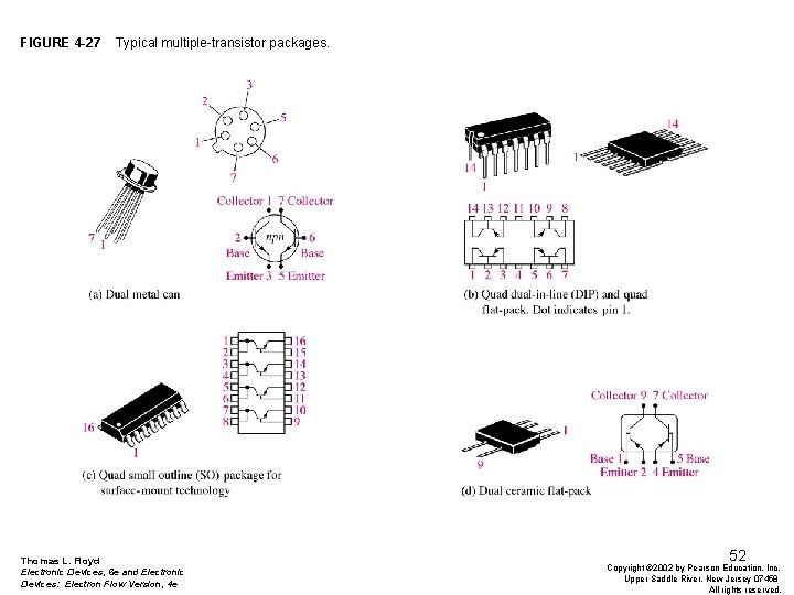
FIGURE 4 -27 Typical multiple-transistor packages. Thomas L. Floyd Electronic Devices, 6 e and Electronic Devices: Electron Flow Version, 4 e 52 Copyright © 2002 by Pearson Education, Inc. Upper Saddle River, New Jersey 07458 All rights reserved.
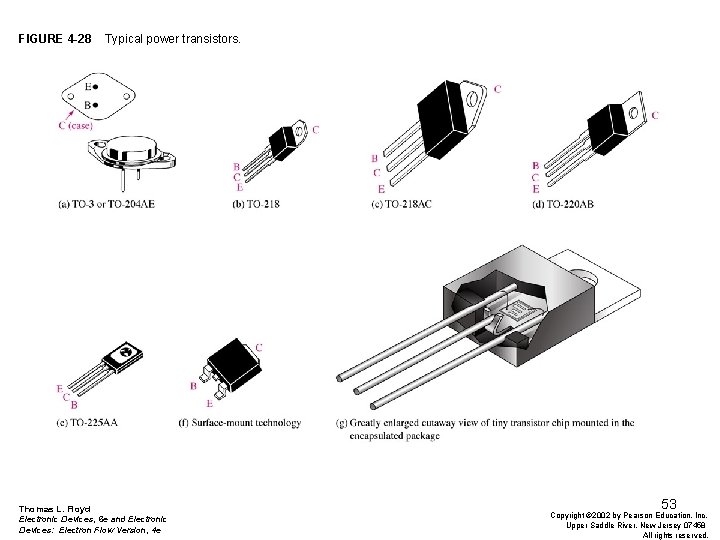
FIGURE 4 -28 Typical power transistors. Thomas L. Floyd Electronic Devices, 6 e and Electronic Devices: Electron Flow Version, 4 e 53 Copyright © 2002 by Pearson Education, Inc. Upper Saddle River, New Jersey 07458 All rights reserved.
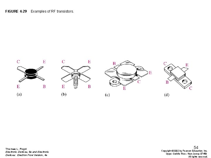
FIGURE 4 -29 Examples of RF transistors. Thomas L. Floyd Electronic Devices, 6 e and Electronic Devices: Electron Flow Version, 4 e 54 Copyright © 2002 by Pearson Education, Inc. Upper Saddle River, New Jersey 07458 All rights reserved.
- Slides: 54